EP0393398B1 - Oszillator in CMOS-Technik - Google Patents
Oszillator in CMOS-Technik Download PDFInfo
- Publication number
- EP0393398B1 EP0393398B1 EP90105978A EP90105978A EP0393398B1 EP 0393398 B1 EP0393398 B1 EP 0393398B1 EP 90105978 A EP90105978 A EP 90105978A EP 90105978 A EP90105978 A EP 90105978A EP 0393398 B1 EP0393398 B1 EP 0393398B1
- Authority
- EP
- European Patent Office
- Prior art keywords
- nmos transistor
- differential amplifier
- source
- terminal
- switching element
- Prior art date
- Legal status (The legal status is an assumption and is not a legal conclusion. Google has not performed a legal analysis and makes no representation as to the accuracy of the status listed.)
- Expired - Lifetime
Links
Images


Classifications
-
- H—ELECTRICITY
- H03—ELECTRONIC CIRCUITRY
- H03K—PULSE TECHNIQUE
- H03K3/00—Circuits for generating electric pulses; Monostable, bistable or multistable circuits
- H03K3/02—Generators characterised by the type of circuit or by the means used for producing pulses
- H03K3/023—Generators characterised by the type of circuit or by the means used for producing pulses by the use of differential amplifiers or comparators, with internal or external positive feedback
- H03K3/0231—Astable circuits
-
- H—ELECTRICITY
- H03—ELECTRONIC CIRCUITRY
- H03K—PULSE TECHNIQUE
- H03K3/00—Circuits for generating electric pulses; Monostable, bistable or multistable circuits
- H03K3/02—Generators characterised by the type of circuit or by the means used for producing pulses
- H03K3/353—Generators characterised by the type of circuit or by the means used for producing pulses by the use, as active elements, of field-effect transistors with internal or external positive feedback
- H03K3/354—Astable circuits
Definitions
- the invention is based on an oscillator using CMOS technology.
- CMOS tilting oscillator (relaxation oscillator) has simple CMOS inverter stages as amplification blocks, which are connected to an external RC resonant circuit. Furthermore, such CMOS tilting oscillators are constructed analogously to emitter-coupled multivibrators by means of a large number of series-connected CMOS inverter stages (Grebene, Alan B., Bipolar and MOS analog integrated circuit design, 1983, ISBN O-471-085 29-4, Chapter 11.5, 11.6) . Such oscillators have the disadvantage that they have a relatively poor temperature stability with increasing frequency and are therefore not usable for high frequencies in the range above 30-50 MHz.
- EP-A-0 180 084 and US-A-4 083 020 disclose CMOS oscillating oscillators with a differential amplifier, a capacitor and a single controllable current source which can be connected to the capacitor.
- the technical object according to the invention consists in a fast temperature and parameter constant controllable oscillator To implement CMOS technology for low to very high frequencies, for example significantly above 100 MHz.
- the oscillator according to the invention can be implemented in monolithically integrated CMOS technology and, because of the technological conditions, has a broad match of the component properties to a semiconductor chip, as well as low input currents of the transistors and a very low current consumption with very high accuracy.
- such an oscillator according to the invention is a cell on a larger CMOS chip, e.g. can be used very universally as part of a PLL (phase locked loop).
- PLL phase locked loop
- the oscillator frequency can be changed completely linearly via the two controllable current sources (current-controlled oscillator principle), with the frequency being varied within very wide limits, i.e. by varying the capacitance. up to 200 MHz, can be changed.
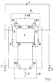
- An oscillator according to the invention constructed in CMOS technology, as shown in FIG. 1, has a differential amplifier D, a first switching unit S1, consisting of a first switching element SE1 and a second switching element SE2, a second switching unit S2, consisting of a third switching element SE3 and a fourth switching element SE4, a first controllable current source I1 and a second controllable current source I2.
- the two controllable current sources I1, I2 are connected together via a capacitor C.
- first current source I1 is connected via a first ohmic resistor R1 to a first input IN1 of the differential amplifier D and the second current source I2 is connected via a second ohmic resistor R2 to a second input IN2 of the differential amplifier D.
- a connection labeled VDD, supply voltage (+ 5V) is connected via the switching path of the first switching element SE1 or via the switching path of the second switching element SE2 with a first tap A1, which is located between the first current source I1 and the first resistor R1, or with a second tap , Tap A2 lying between the second current source I2 and the second resistor R2.
- a first output OUT1 and a second output OUT2 of the differential amplifier D are connected to a switching input of the first switching element SE1 and to a switching input of the second switching element SE2.
- Either the first input IN1 or the second input IN2 of the differential amplifier D can be connected via a switching path of the third switching element SE3 or via a switching path of the fourth switching element SE4 to a third current source I4 which is likewise constructed using CMOS technology.
- a control input of the third switching element SE3 and a control input of the fourth switching element SE4 are connected to the first output OUT1 and to the second output OUT2 of the differential amplifier D.
- the first switching unit S1 comprises a first NMOS transistor N1 forming the first switching element SE1 and a second NMOS transistor N2 forming the second switching element SE2, and a first and a second current mirror circuit.
- the first current mirror circuit is constructed from a first PMOS transistor P1 and a second PMOS transistor P2.
- the two drain connections are connected to the supply voltage connection VDD.
- the two gate connections are interconnected and the source connection of the second PMOS transistor P2 is on the interconnected gate connections fed back and connected to the drain of the first NMOS transistor N1.
- the source terminal of the first PMOS transistor P1 is connected to the first tap A1.
- the second current mirror circuit consists of a third PMOS transistor P3 and a fourth PMOS transistor P4 and is constructed symmetrically to the first current mirror circuit and correspondingly connected to the second NMOS transistor N2 (source connection from P3 to drain connection from N2) and the second tap A2 ( connected to the source of P4).
- the source connections of the first and second NMOS transistors N1, N2 are connected together and connected to the fourth current source I4.
- the gate connection of the first NMOS transistor N1 and the gate connection of the second NMOS transistor N2 form the control input of the first switching element SE1 and the control input of the second switching element SE2 (see FIG. 1).
- the second switching unit S2 has a third NMOS transistor N3 forming the third switching element and a fourth NMOS transistor N4 forming the fourth switching element.
- the drain terminal of the third NMOS transistor N3 and the drain terminal of the fourth NMOS transistor N4 are connected to the terminal of the first resistor R1 facing away from the first tap A1 and to the terminal of the second resistor R2 facing away from the second tap A2.
- the two source connections are connected together and connected to the third current source I3.
- the gate terminal of the third NMOS transistor N3 and the gate terminal of the fourth NMOS transistor N4 form the control input of the third switching element SE3 or the control input of the fourth switching element SE4 (cf. FIG. 1).
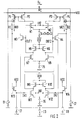
- the differential amplifier D is designed according to Figure 2 as a cascaded two-stage amplifier circuit.
- a first differential amplifier stage consists of a fifth, sixth, seventh and eighth NMOS transistor N5, N6, N7, N8 and a fifth current source I5 constructed using CMOS technology.
- a second differential amplifier stage consists of a ninth, tenth, eleventh and twelfth NMOS transistor N9, N10, N11, N12 and a sixth current source I6 constructed using CMOS technology.
- the drain connections and the interconnected gate connections of N5 and N6 are connected to the supply voltage connection VDD.
- the source connection of N5 and the Sorucean connection of N6 form the first output OUT1 and the second output OUT2 of the differential amplifier D (see also FIG. 1).
- the two transistors N5, N6 represent the two load resistors of a conventional differential amplifier.
- the source connections of N7 and N8 are connected together and connected to the fifth current source I5.
- the drain of N7 and the drain of N8 are connected to the source of N5 and the source of N6, respectively.
- the gate connection of N7 and the gate connection of N8 form a first output and a second output of the first differential amplifier stage.
- the two NMOS transistors represent the first amplifier stage of the differential amplifier.
- the second differential amplifier stage is constructed analogously to the first differential amplifier stage, the ninth NMOS transistor N9 and the tenth NMOS transistor N10 correspondingly representing the two load resistors and the eleventh NMOS transistor N11 and the twelfth NMOS transistor N12 forming the actual second amplifier stage (cf. Figure 2).
- the drain connection of N11 and the drain connection of N12 are connected to the second output and the first output of the first differential amplifier stage. Furthermore, the gate connection of N11 and the gate connection of N12 form the first input IN1 and the second input IN2 of the differential amplifier D.
- the first controllable current source I1 and the second controllable current source I2 are connected together via the frequency-determining capacitor C.
- the first current source I1 and the second current source I2 are connected via the first resistor R1 to the drain terminal of N3 and via the second resistor R2 to the drain terminal of N4.
- the first resistor R1 with its connection facing away from the first tap A1 is the gate terminal of a thirteenth NMOS transistor N13 and the second resistor R2 with its terminal facing away from the second tap A2 is the gate terminal of a fourteenth NMOS transistor N14 connected.
- the drain connection of N13 and the drain connection of N14 are connected to the supply voltage-carrying connection VDD.
- the source connection of N13 is with the gate connection of N11, ie with the first input IN1 of the differential amplifier D and connected to a seventh current source I7 constructed using CMOS technology.
- the source connection of N14 is connected to the gate connection of N12, ie to the second input IN2 of the differential amplifier D, and to an eighth current source I8 constructed using CMOS technology.
- the thirteenth NMOS transistor N13 and the fourteenth NMOS transistor N11 form so-called source follower stages which, compared to the subsequent differential amplifier transistors N11 and N12, have an input capacitance that is about a factor of 5 to 10 smaller, so that the first ohmic resistor R1 and RC product formed via the second ohmic resistor R2 becomes negligibly small.
- the seventh current source I7 and the eighth current source I8 are used to set the operating points of N13 and N14, respectively.
- N13 and N14 By controlling N13 and N14 by means of the currents I7 and I8, a gate-source voltage is built up at N13 and N14, which enables the subsequent differential amplifier transistors N11, N12 to operate in the pinch-off region of the transistor characteristic, which due to its higher steepness and therefore reinforcement is preferable to the start-up range of the characteristic.
- the current source has two NMOS transistors N15, N16 connected as current mirrors, N15 forming the output current path for the second current source.
- the output currents I1 and I2 of the two current sources are, in accordance with the mirror ratio, proportional to the control current, a mirror ratio of 1, ie output currents I1 and I2 of equal size, being selected here for the symmetrical design of the oscillator.
- the oscillator frequency can be changed linearly via the currents I1 and I2.
- the oscillator works with a supply voltage VDD of + 5V.
- the two controlled current sources deliver a current in the milliampere range, and the voltage swing of the circuit (voltage drop across the resistors) is in the range of a few hundred millivolts.
- the differential amplifier stages each have an amplification factor in the range from 2 to 10, and to achieve frequencies substantially above 100 MHz, the capacitor C has a capacitance in the picofarad range.
- the fourth current source I4 is dimensioned in such a way that it delivers a current I4, which is somewhat larger than the sum of the amounts of the first, second and third current sources (cf. FIG. 2).
- the second line - b - shows the voltage curve U12 between the first and second switching elements SE1, SE2 of the first switching unit S1 over time t (for U12, cf. FIG. 2).
- the third line - c - shows the voltage swing UR1 at the first ohmic resistor R1 over the time axis t and in the fourth row - d - shows the voltage swing UR2 at the second ohmic resistor R2 above the time axis t.
- the fifth line - e - shows the voltage curve U87 at the differential amplifier inputs IN1, IN2 over time t.
- the time axis t is divided into the time intervals 0, 1/4, 1/2, 3/4 ... of the time period T of the oscillator frequency f.
- the previously described oscillator can be used between very low frequencies and around 200 MHz. It enables linear control of the output frequency over a wide range. Compared to conventional bipolar oscillators, it is characterized by very low power consumption and much higher accuracy. Furthermore, compared to known CMOS oscillators, it has a much better temperature and parameter consistency due to its simple symmetrical structure, since the individual influencing factors cancel each other out. In addition, a frequency range that is higher by a power of ten can be set.
- CMOS circuit can be integrated on highly integrated, digital CMOS chips, which previously required additional bipolar voltage-controlled oscillators (VCO) to achieve the necessary accuracy and very high frequencies.
- VCO voltage-controlled oscillators
- the previously described oscillator can also be constructed in a complementary manner (i.e. NMOS transistors are used instead of PMOS and vice versa).
Landscapes
- Inductance-Capacitance Distribution Constants And Capacitance-Resistance Oscillators (AREA)
- Amplifiers (AREA)
- Logic Circuits (AREA)
- Oscillators With Electromechanical Resonators (AREA)
- Stabilization Of Oscillater, Synchronisation, Frequency Synthesizers (AREA)
- Manipulation Of Pulses (AREA)
- Polymers With Sulfur, Phosphorus Or Metals In The Main Chain (AREA)
Description
- Die Erfindung geht von einem Oszillator in CMOS-Technik aus.
- Ein bekannter CMOS-Kipposzillator (relaxation oscillator) weist einfache CMOS-Inverterstufen als Verstärkungsblöcke auf, die mit einem externen RC-Schwingkreis beschaltet werden. Ferner werden solche CMOS-Kipposzillatoren analog zu emittergekoppelten Multivibratoren mittels einer Vielzahl hintereinandergeschalteter CMOS-Inverterstufen aufgebaut (Grebene, Alan B., Bipolar and MOS analog integrated circuit design, 1983, ISBN O-471-085 29-4, Chapter 11.5, 11.6). Solche Oszillatoren haben den Nachteil, daß sie mit zunehmender Frequenz eine relativ schlechte Temperaturstabilität aufweisen und somit für hohe Frequenzen im Bereich über 30 - 50 MHz nicht brauchbar sind.
- Die Druckschriften EP-A-0 180 084 und US-A-4 083 020 offenbaren CMOS-Kipposzillatoren mit einem Differenzverstärker, einem Kondensator und einer einzigen steuerbaren Stromquelle, die mit dem Kondensator verbindbar ist.
- Die technische Aufgabe gemäß der Erfindung besteht darin, einen schnellen temperatur- und parameter-konstanten steuerbaren Oszillator in CMOS-Technik für niedrige bis zu sehr hohen Frequenzen, z.B. deutlich über 100 MHz, zu realisieren.
- Diese Aufgabe wird erfindungsgemäß durch die Lehre des unabhängigen Anspruchs gelöst.
- Der erfindungsgemäße Oszillator ist in monolithisch integrierter CMOS-Technologie realisierbar und weist aufgrund der technologischen Gegebenheiten eine weitgehende Übereinstimmung der Bauelementeeigenschaften auf einen Halbleiterchip, sowie geringe Eingangsströme der Transistoren und einen sehr geringen Stromverbrauch bei gleichzeitig sehr großer Genauigkeit auf.
- Insbesondere ist ein solcher erfindungsgemäßer Oszillator als Zelle auf einem größeren CMOS-Chip, z.B. als Bestandteil einer PLL (phase locked loop) sehr universell einsetzbar.
- Über die beiden steuerbaren Stromquellen kann die Oszillatorfrequenz völlig linear geändert werden (stromgesteuertes Oszillatorprinzip), wobei durch Variation der Kapazität die Frequenz in sehr weiten Grenzen, d.h. bis zu 200 MHz, verändert werden kann.
- Weitere vorteilhafte Ausgestaltungen des Gegenstands der Erfindung sind den abhängigen Ansprüchen zu entnehmen.
- Ein Ausführungsbeispiel wird im folgenden anhand der Zeichnungen erläutert. Es zeigen:
- Fig. 1
- ein Prinzipschaltbild des erfindungsgemäßen Oszillators,
- Fig. 2
- ein detailliertes Schaltbild des erfindungsgemäßen Oszillators,
- Fig. 3
- ein Schaltbild einer steuerbaren Stromquelle gemäß der Erfindung und
- Fig. 4
- Zeitdiagramm zur Erläuterung der Funktionsweise des erfindungsgemäßen Oszillators.
- Ein in CMOS-Technologie aufgebauter erfindungsgemäßer Oszillator, wie in Figur 1 gezeigt, weist einen Differenzverstärker D, eine erste Schalteinheit S1, bestehend aus einem ersten Schaltelement SE1 und einem zweiten Schaltelement SE2, eine zweite Schalteinheit S2, bestehend aus einem dritten Schaltelement SE3 und aus einem vierten Schaltelement SE4, eine erste steuerbare Stromquelle I1 und eine zweite steuerbare Stromquelle I2 auf. Die beiden steuerbaren Stromquellen I1, I2 sind über einen Kondensator C zusammengeschaltet.
- Weiterhin ist die erste Stromquelle I1 über einen ersten ohmschen Widerstand R1 mit einem ersten Eingang IN1 des Differenzverstärkers D und die zweite Stromquelle I2 über eine zweiten ohmschen Widerstand R2 mit einem zweiten Eingang IN2 des Differenzverstärkers D verbunden.
- Ein mit VDD bezeichneter, Versorgungsspannung (+5V) führender Ansschluß ist über den Schaltweg des ersten Schaltelements SE1 oder über den Schaltweg des zweiten Schaltelements SE2 mit einem ersten, zwischen der ersten Stromquelle I1 und dem ersten Widerstand R1 liegenden Abgriff A1 bzw. mit einem zweiten, zwischen der zweiten Stromquelle I2 und dem zweiten Widerstand R2 liegenden Abgriff A2 verbindbar.
- Ferner ist ein erster Ausgang OUT1 und ein zweiter Ausgang OUT2 des Differenzverstärkers D mit einem Schalteingang des ersten Schaltelements SE1 bzw. mit einem Schalteingang des zweiten Schaltelementes SE2 verbunden.
- Entweder der erste Eingang IN1 oder der zweite Eingang IN2 des Differenzverstärkers D sind über einen Schaltweg des dritten Schaltelementes SE3 bzw. über einen Schaltweg des vierten Schaltelementes SE4 mit einer dritten, ebenfalls in CMOS-Technik aufgebauten Stromquelle I4 verbindbar. Ein Steuereingang des dritten Schaltelements SE3 und ein Steuereingang des vierten Schaltelementes SE4 sind mit dem ersten Ausgang OUT1 bzw. mit dem zweiten Ausgang OUT2 des Differenzverstärkers D verbunden.
- Im folgenden wird anhand der Figur 2 detailliert eine mögliche Ausführungsform des erfindungsgemäßen Oszillators beschrieben.
- Die erste Schalteinheit S1 besteht aus einem das erste Schaltelement SE1 bildenden ersten NMOS-Transistor N1 und aus einem das zweite Schaltelement SE2 bildenden zweiten NMOS-Transistor N2, sowie aus einer ersten und einer zweiten Stromspiegelschaltung.
- Die erste Stromspiegelschaltung ist aus einem ersten PMOS-Transistor P1 und einem zweiten PMOS-Transistor P2 aufgebaut. Die beiden Drainanschlüsse sind mit dem Versorgungsspannung führenden Anschluß VDD verbunden. Die beiden Gateanschlüsse sind zusammengeschaltet und der Sourceanschluß des zweiten PMOS-Transistors P2 ist auf die zusammengeschalteten Gateanschlüsse zurückgekoppelt sowie mit dem Drainanschluß des ersten NMOS-Transistors N1 verbunden. Der Sourceanschluß des ersten PMOS-Transistors P1 ist mit dem ersten Abgriff A1 verbunden.
- Die zweite Stromspiegelschaltung besteht aus einem dritten PMOS-Transistor P3 und einem vierten PMOS-Transistor P4 und ist symmetrisch zur ersten Stromspiegelschaltung aufgebaut und entsprechend mit dem zweiten NMOS-Transistor N2 (Sourceanschluß von P3 an Drainanschluß von N2) und dem zweiten Abgriff A2 (verbunden mit dem Sourceanschluß von P4) verbunden.
- Die Sourceanschlüsse des ersten und zweiten NMOS-Transistors N1, N2 sind zusammengeschaltet und mit der vierten Stromquelle I4 verbunden. Der Gateanschluß des ersten NMOS-Transistors N1 und der Gateanschluß des zweiten NMOS-Transistors N2 bilden den Steuereingang des ersten Schaltelements SE1 bzw. den Steuereingang des zweiten Schaltelements SE2 (vgl. Figur 1).
- Die zweite Schalteinheit S2 weist einen das dritte Schaltelement bildenden dritten NMOS-Transistor N3 und einen das vierte Schaltelement bildenden vierten NMOS-Transistor N4 auf. Der Drainanschluß des dritten NMOS-Transistors N3 und der Drainanschluß des vierten NMOS-Transistors N4 sind mit dem von dem ersten Abgriff A1 abgewandten Anschluß des ersten Widerstandes R1 bzw. mit dem von dem zweiten Abgriff A2 abgewandten Anschluß des zweiten Widerstandes R2 verbunden. Weiterhin sind die beiden Sourceanschlusse (von N3 und N4) zusammengeschaltet und mit der dritten Stromquelle I3 verbunden. Der Gateanschluß des dritten NMOS-Transistors N3 und der Gateanschluß des vierten NMOS-Transistors N4 bilden den Steuereingang des dritten Schaltelements SE3 bzw. den Steuereingang des vierten Schaltelements SE4 (vgl. Figur 1).
- Der Differenzverstärker D ist gemäß Figur 2 als kaskadierte zweistufige Verstärkerschaltung ausgelegt. Eine erste Differenzverstärkerstufe besteht aus einem fünften, sechsten, siebten und achten NMOS-Transistor N5, N6, N7, N8 sowie aus einer fünften, in CMOS-Technik aufgebauten Stromquelle I5. Analog dazu besteht eine zweite Differenzverstärkerstufe aus einem neunten, zehnten, elften und zwölften NMOS-Transistor N9, N10, N11, N12 sowie aus einer sechsten, in CMOS-Technik aufgebauten Stromquelle I6.
- Die Drainanschlüsse sowie die zusammengeschalteten Gateanschlüsse von N5 und N6 sind mit dem Versorgungsspannungsanschluß VDD verbunden. Der Sourceanschluß von N5 und der Soruceanschluß von N6 bilden den erSten Ausgang OUT1 bzw. den zweiten Ausgang OUT2 des Differenzverstärkers D (vgl. auch Figur 1). Die beiden Transistoren N5, N6 stellen die beiden Lastwiderstände eines üblichen Differenzverstärkers dar. Die Sourceanschlüsse von N7 und N8 sind zusammengeschaltet und mit der fünften Stromquelle I5 verbunden. Der Drainanschluß von N7 und der Drainanschluß von N8 ist mit dem Sourceanschluß von N5 bzw. mit dem Sourceanschluß von N6 verbunden. Der Gateanschluß von N7 und der Gateanschluß von N8 bilden einen ersten Ausgang bzw. einen zweiten Ausgang der ersten Differenzverstärkerstufe. Die beiden NMOS-Transistoren stellen dabei die erste Verstärkerstufe des Differenzverstärkers dar.
- Die zweite Differenzverstärkerstufe ist analog zur ersten Differenzverstärkerstufe aufgebaut, wobei der neunte NMOS-Transistor N9 und der zehnte NMOS-Transistor N10 entsprechend die beiden Lastwiderstände darstellen und der elfte NMOS-Transistor N11 und der zwölfte NMOS-Transistor N12 die eigentliche zweite Verstärkerstufe bilden (vgl. Figur 2).
- Der Drainanschluß von N11 und der Drainanschluß von N12 sind mit dem zweiten Ausgang bzw. dem ersten Ausgang der ersten Differenzverstärkerstufe verbunden. Ferner bilden der Gateanschluß von N11 und der Gateanschluß von N12 den ersten Eingang IN1 bzw. den zweiten Eingang IN2 des Differenzverstärkers D.
- Weiterhin sind, wie Figur 2 zeigt, die erste steuerbare Stromquelle I1 und die zweite steuerbare Stromquelle I2 über den frequenzbestimmenden Kondensator C zusammengeschaltet. Die erste Stromquelle I1 und die zweite Stromquelle I2 sind über den ersten Widerstand R1 mit dem Drainanschluß von N3 bzw. über den zweiten Widerstand R2 mit dem Drainanschluß von N4 verbunden.
- Gemäß einer vorteilhaften Ausgestaltung der Erfindung ist der erste Widerstand R1 mit seinem dem ersten Abgriff A1 abgewandten Anschluß mit dem Gateanschluß eines dreizehnten NMOS-Transistors N13 und der zweite Widerstand R2 mit seinem dem zweiten Abgriff A2 abgewandten Anschluß mit dem Gateanschluß eines vierzehnten NMOS-Transistors N14 verbunden. Der Drainanschluß von N13 und der Drainanschluß von N14 sind mit dem Versorgungsspannung führenden Anschluß VDD verbunden. Der Sourceanschluß von N13 ist mit dem Gateanschluß von N11, d.h. mit dem ersten Eingang IN1 des Differenzverstärkers D sowie mit einer siebten, in CMOS-Technik aufgebauten Stromquelle I7 verbunden. Analog dazu ist der Sourceanschluß von N14 mit dem Gateanschluß von N12, d.h. mit dem zweiten Eingang IN2 des Differenzverstärkers D, sowie mit einer achten, in CMOS-Technik aufgebauten Stromquelle I8 verbunden.
- Der dreizehnte NMOS-Transistor N13 und der vierzehnte NMOS-Transistor N11 bilden sogenannte Sourcefolgerstufen, die gegenüber den nachfolgenden Differenzverstärker-Transistoren N11 bzw. N12 eine um etwa den Faktor 5 bis 10 kleinere Eingangskapazität aufweisen, so daß das über den ersten ohmschen Widerstand R1 bzw. über den zweiten ohmschen Widerstand R2 gebildete RC-Produkt vernachlässigbar klein wird.
- Die siebte Stromquelle I7 und die achte Stromquelle I8 dienen zur Arbeitspunkteinstellung von N13 bzw. N14. Durch die Ansteuerung von N13 und N14 mittels der Ströme I7 bzw. I8 wird eine Gate-Source-Spannung an N13 bzw. N14 aufgebaut, die den Betrieb der nachfolgenden Differenzverstärker-Transistoren N11, N12 im Abschnürbereich der Transistorkennlinie ermöglicht, welcher infolge seiner höheren Steilheit und damit Verstärkung dem Anlaufbereich der Kennlinie vorzuziehen ist.
- Ein Aufbau der steuerbaren Stromquelle I1, I2 wird im folgenden anhand der Figur 3 erläutert. Die Stromquelle weist zwei als Stromspiegel geschaltete NMOS-Transistoren N15, N16 auf, wobei N15 den Ausgangsstrompfad für die zweite Stromquelle bildet. Ein siebzehnter NMOS-Transistor N17, dessen Gateanschluß mit dem Gateanschluß von N16 verbunden ist, bildet den Ausgangsstrompfad für die erste Stromquelle I1. Die Ausgangsströme I1 und I2 der beiden Stromquellen sind, entsprechend dem Spiegelverhältnis, proportional zum Steuerstrom, wobei hier zur symmetrischen Auslegung des Oszillators ein Spiegelverhältnis von 1, d.h. gleich große Ausgangsströme I1 und I2, gewählt werden. Über die Ströme I1 und I2 kann die Oszillatorfrequenz linear geändert werden.
- Der Oszillator arbeitet mit einer Versorgungsspannung VDD von +5V. Ferner sind die beiden ohmschen Widerstände R1, R2 betragsgemäß gleich groß zu R1 = R2 = 1 k gewählt. Die beiden gesteuerten Stromquellen geben einen Strom im Milliampère-Bereich ab, und der Spannungshub der Schaltung (Spannungsabfall an den Widerständen) liegt im Bereich von einigen hundert Millivolt. Außerdem weisen die Differenzverstärkerstufen je einen Verstärkungsfaktor im Bereich von 2 bis 10 auf, und zur Erreichung von Frequenzen wesentlich oberhalb von 100 MHz weist der Kondensator C eine Kapazität im Picofarad-Bereich auf. Ferner ist die vierte Stromquelle I4 so dimensioniert, daß sie betragsmäßig einen Strom I4 liefert, der etwas größer ist, als die Summe der Beträge der ersten, der zweiten und der dritten Stromquelle (vgl. Figur 2).
- Die Erläuterung der Funktion des erfindungsgemäßen Oszillators erfolgt nun mit Hilfe der Zeitdiagramme der Figur 4.
- In der ersten Zeile - a - ist der Spannungsverlauf UC am Kondensator C über der Zeit t dargestellt, wobei die Kondensatorspannung UC in einem ersten Umschaltpunkt gleich dem Spannungsabfall am ersten Widerstand


- In der zweiten Zeile - b - ist der Spannungsverlauf U12 zwischen dem ersten und dem zweiten Schaltelement SE1, SE2 der ersten Schalteinheit S1 über der Zeit t dargestellt (zu U12, vgl. Figur 2).
- In der dritten Zeile - c - ist der Spannungshub UR1 am ersten ohmschen Widerstand R1 über der Zeitachse t und in der vierten Zeile - d - ist der Spannungshub UR2 am zweiten ohmschen Widerstand R2 über der Zeitachse t aufgezeigt.
- Schließlich ist in der fünften Zeile - e - der Spannungsverlauf U87 an den Differenzverstärkereingängen IN1, IN2 über der Zeit t dargestellt. Die Zeitachse t ist jweils in die Zeitabstände 0, 1/4, 1/2, 3/4 ... der Zeitdauer T der Oszillatorfrequenz f unterteilt. Die Oszillatorfrequenz f berechnet sich bei einem symmetrischen Schaltungsaufbau (d.h.


- Ausgehend von einem ungeladenen Kondensator C (UC = 0) und von einem Zeitpunkt t = 0 (vgl. Figur 4) ist in einem ersten Kippzustand ein erster Strompfad aus erster Stromspiegelschaltung P1, P2, aus erstem Schaltelement N1 (vgl. Figur 4b, U12 > 0) und aus erster Differenzverstärkerstufe (N7 leitend) und zweiter Differenzverstärkerstufe (N12 leitend) durchgeschaltet (U87 > 0 in Fig. 4e). Dies bewirkt, daß das dritte Schaltelement SE3, d.h. der dritte NMOS-Transistor N3, ebenfalls leitend ist, so daß am ersten Widerstand R1 eine Spannung

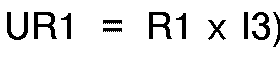
- Dadurch, daß der vierte NMOS-Transistor N4 (vgl. Figur 2) in dem ersten Kippzustand nicht leitend ist und bei gleichzeitiger Voraussetzung, daß N13 und N14 gleichartig sind und damit den gleichen Gate-Source-Spannungsabfall aufweisen, ist zunächst zum Zeitpunkt t = 0 der Spannungsabfall UR1 am ersten Widerstand R1 gleich dem Spannungsabfall U87 zwischen den Differenzverstärkereingängen (vgl. Figur 4c und 4e).
- Da P1 leitend ist und gleichzeitig P4, d.h. die zweite Stromspiegelschaltung nicht leitend ist (U12 > 0), wird jetzt der Kondensator C durch den Strom I2 der zweiten Stromquelle I2 aufgeladen (vgl. Figur 4a). Entsprechend verringert sich die Spannung U87 an den Differenzverstärkereingängen (vgl. Figur 4e), und zwar bis zum Zeitpunkt


- Jetzt "kippt" die Schaltung in den zweiten Kippzustand um. Da jetzt U12 < 0 gilt, ist der erste Strompfad gesperrt und ein zweiter Strompfad aus zweiter Stromspiegelschaltung P3, P4 aus zweitem NMOS-Transistor N2, d.h. zweites Schaltelement SE2, und aus erster Differenzverstärkerstufe (N8 leitend) sowie zweiter Differenzverstärkerstufe (N11 leitend) durchgeschaltet (vgl. Fig. 4b, 4e, da U87 < 0). Am zweiten Widerstand R2 fällt jetzt die Spannung

- Somit wird der Kondensator C entladen (vgl. Fig. 4a), und zwar solange, bis zum Zeitpunkt



- Der zuvor geschilderte Oszillator ist zwischen sehr niedrigen Frequenzen und etwa 200 MHz einsetzbar. Er ermöglicht eine in weiten Bereichen lineare Steuerung der Ausgangsfrequenz. Er zeichnet sich gegenüber herkömmlichen Bipolar-Oszillatoren durch einen sehr geringen Stromverbrauch und eine wesentlich höhere Genauigkeit aus. Ferner weist er im Vergleich zu bekannten CMOS-Oszillatoren aufgrund seines einfachen symmetrischen Aufbaus eine wesentlich bessere Temperatur- und Parameterkonstanz auf, da sich die einzelnen Einflußfaktoren gegenseitig aufheben. Außerdem ist ein um eine Zehnerpotenz höherer Frequenzbereich einstellbar.
- Ein besonderer Vorteil liegt in der Integrierbarkeit dieser CMOS-Schaltung auf hochintegrierten, digitalen CMOS-Chips, welche bisher zusätzlich externe bipolare spannungsgesteuerte Oszillatoren (VCO) zum Erreichen der notwendigen Genauigkeit und der sehr hohen Frequenzen benötigten.
- Selbstverständlich kann der zuvor geschilderte Oszillator auch komplementär aufgebaut werden (d.h. anstelle PMOS- werden NMOS-Transistoren verwendet und umgekehrt).
Claims (10)
- Oszillator in CMOS-Technik, mit- einem Differenzverstärker (D),- einer ersten Schalteinheit (S1) aus einem ersten Schaltelement (SE1) und einem zweiten Schaltelement (SE2),- einer zweiten Schalteinheit (S2) aus einem dritten Schaltelement (SE3) und einem vierten Schaltelement (SE4)- einer ersten (I1) und einer zweiten steuerbaren Stromquelle (I2), die über einen Kondensator (C) zusammengeschaltet sind,- und mit einem Aufbau wie folgt- die erste Stromquelle (I1) ist über einen ersten ohmschen Widerstand (R1) mit einem ersten Eingang (IN1) des Differenzverstärkers (D) verbunden und die zweite Stromquelle (I2) ist über einen zweiten ohmschen Widerstand (R2) mit einem zweiten Eingang (IN2) des Differenzverstärkers (D) verbunden,- ein Versorgungsspannung führender Anschluß (VDD) ist über den Schaltweg des ersten Schaltelementes (SE1) mit einem ersten, zwischen der ersten Stromquelle (I1) und dem ersten Widerstand (R1) liegenden Abgriff (A1) verbindbar und über den Schaltweg des zweiten Schaltelementes (SE2) mit einem zweiten, zwischen der zweiten Stromquelle (I2) und dem zweiten Widerstand (R2) liegenden Abgriff (A2) verbindbar,- ein erster Ausgang (OUT1) des Differenzverstärkers (D) ist mit einem Schalteingang des ersten Schaltelementes (SE1) verbunden und ein zweiter Ausgang (OUT2) des Differenzverstärkers (D) ist mit einem Schalteingang des zweiten Schaltelementes (SE2) verbunden,- der erste Eingang (IN1) des Differenzverstärkers (D) ist über einen Schaltweg des dritten Schaltelements (SE3) und der zweite Eingang (IN2) des Differenzverstärkers (D) ist über einen Schaltweg des vierten Schaltelements (SE4) mit einer dritten, in CMOS-Technik aufgebauten Stromquelle (I3) verbindbar,
und- ein Steuereingang des dritten Schaltelementes (SE3) ist mit dem ersten Ausgang (OUT1) des Differenzverstärkers (D) und ein Steuereingang des vierten Schaltelementes (SE4) ist mit dem zweiten Ausgang (OUT2) des Differenzverstärkers (D) verbunden. - Oszillator nach Anspruch 1, mit folgender Merkmalskombination- die erste Schalteinheit (S1) ist aus einem das erste Schaltelement (SE1) bildenden ersten NMOS-Transistor (N1), aus einem das zweite Schaltelement (SE2) bildenden zweiten NMOS-Transistor (N2), aus einer aus einem ersten PMOS-Transistor (P1) und einem zweiten PMOS-Transistor (P2) aufgebauten ersten Stromspiegelschaltung und aus einer aus einem dritten PMOS-Transistor (P3) und einem vierten PMOS-Transistor (P4) aufgebauten zweiten Stromspiegelschaltung aufgebaut,- der Ausgangsstromzweig (Drain von P1) der ersten Stromspiegelschaltung ist mit dem ersten Abgriff (A1) und der Ausgangsstromzweig (Drain von P4) der zweiten Stromspiegelschaltung ist mit dem zweiten Abgriff (A2) verbunden,- der Referenzstromzweig der ersten Stromspiegelschaltung ist über den Schaltweg des ersten NMOS-Transistors (N1) und der Referenzstromzweig der zweiten Stromspiegelschaltung ist über den Schaltweg des zweiten NMOS-Transistors (N2) mit einer vierten, in CMOS-Technik aufgebauten Stromquelle (I4) verbindbar und- der Gateanschluß des ersten NMOS-Transistors (N1) bildet den Steuereingang des ersten Schaltelementes (SE1) und der Gateanschluß des zweiten NMOS-Transistors (N2) bildet den Steuereingang des zweiten Schaltelementes (SE2).
- Oszillator nach Anspruch 1 oder 2, mit folgender Merkmalskombination- die zweite Schalteinheit (S2) ist aus einem das dritte Schaltelement (SE3) bildenden dritten NMOS-Transistor (N3) und aus einem das vierte Schaltelement (SE4) bildenden vierten NMOS-Transistor (N4) aufgebaut,- der erste Widerstand (R1) ist über den Schaltweg des dritten NMOS-Transistors (N3) und der zweite Widerstand (R2) ist über den Schaltweg des vierten NMOS-Transistors (N4) mit der dritten Stromquelle (I3) verbindbar und- der Gateanschluß des dritten NMOS-Transistors (N3) ist mit dem ersten Ausgang (OUT1) verbunden und der Gateanschluß des vierten NMOS-Transistors (N4) ist mit dem zweiten Ausgang (OUT2) des Differenzverstärkers (D) verbunden.
- Oszillator nach einem der vorhergehenden Ansprüche, mit folgender Merkmalskombination- der Differenzverstärker (D) ist aus einer ersten Differenzverstärkerstufe (N5, N6, N7, N8, 15) und aus einer zweiten Differenzverstärkerstufe (N9, N10, N11, N12, 16) aufgebaut, die in Kaskade geschaltet sind.
- Oszillator nach Anspruch 4, mit folgender Merkmalskombination- die erste Differenzverstärkerstufe enthält einen fünften NMOS-Transistor (N5) und einen sechsten NMOS-Transistor (N6), deren Gateanschlüsse und deren Drainanschlüsse mit dem Versorgungsspannung führenden Anschluß (VDD) verbunden sind,- der Sourceanschluß des fünften NMOS-Transistors (N5) bildet den ersten Ausgang (OUT1) und der Sourceanschluß des sechsten NMOS-Transistors (N6) bildet den zweiten Ausgang (OUT2) des Differenzverstärkers (D),- die erste Differenzverstärkerstufe enthält einen siebten (N7) und einen achten NMOS-Transistor, deren Sourceanschlüsse mit einer in CMOS-Technik aufgebauten fünften Stromquelle (I5) verbunden sind,- der Drainanschluß des siebten NMOS-Transistors (N7) ist mit dem Sourceanschluß des fünften des fünften NMOS-Transistors (N5) verbunden und der Drainanschluß des achten NMOS-Transistors (N8) ist mit dem Sourceanschluß des sechsten NMOS-Transistors (N6) verbunden und- der Gateanschluß des siebten NMOS-Transistors (N7) bildet einen ersten Eingang und der Gateanschluß des achten NMOS-Transistors (N8) bildet einen zweiten Eingang der ersten Differenzverstärkerstufe.
- Oszillator nach Anspruch 5, mit folgender Merkmalskombination- die zweite Differenzverstärkerstufe enthält einen neunten NMOS-Transistor (N9) und einen zehnten NMOS-Transistor (N10), deren Gateanschlüsse und deren Drainanschlüsse mit dem Versorgungsspannung führenden Anschluß (VDD) verbunden sind,- der Sourceanschluß des neunten (N9) ist mit dem zweiten Eingang und der Sourceanschluß des zehnten NMOS-Transistors (N10) ist mit dem ersten Eingang der ersten Differenzverstärkerstufe (N5, N6, N7, N8, 15) verbunden,- die zweite Differenzverstärkerstufe enthält einen elften NMOS-Transistor (N11) und einen zwölften NMOS-Transistor (N12), deren Sourceanschlüsse mit einer in CMOS-Technik aufgebauten sechsten Stromquelle (I6) verbunden sind,- der Drainanschluß des elften NMOS-Transistors (N11) ist mit dem Sourceanschluß des neunten NMOS-Transistors (N9) verbunden und der Drainanschluß des zwölften NMOS-Transistors (N12) ist mit dem Sourceanschluß des zehnten NMOS-Transistors (N10) verbunden und- der Gateanschluß des elften NMOS-Transistors (N11) bildet den ersten Eingang (IN1) und der Gateanschluß des zwölften NMOS-Transistors (N12) bildet den zweiten Eingang (IN2) des Differenzverstärkers (D).
- Oszillator nach einem der vorhergehenden Ansprüche, mit folgender Merkmalskombination- der dem ersten Abgriff (A1) abgewandte Anschluß des ersten Widerstandes (R1) ist mit dem Gateanschluß eines dreizehnten NMOS-Transistors (N13) verbunden und der dem zweiten Abgriff (A2) abgewandte Anschluß des zweiten Widerstandes (R2) ist mit dem Gateanschluß eines vierzehnten NMOS-Transistors (N14) verbunden,- die Drainanschlüsse des dreizehnten und vierzehnten NMOS-Transistors (N14) sind mit dem Versorgungsspannung führenden Anschluß (VDD) verbunden,- der Sourceanschluß des dreizehnten NMOS-Transistors (N13) ist mit dem ersten Eingang (IN1) des Differenzverstärkers (D) und mit einer in CMOS-Technik aufgebauten siebten Stromquelle (I7) verbunden und- der Sourceanschluß des vierzehnten NMOS-Transistors (N14) ist mit dem zweiten Eingang (IN2) des Differenzverstärkers (D) und mit einer in CMOS-Technik aufgebauten achten Stromquelle (I8) verbunden.
- Oszillator nach Anspruch 2, der so dimensioniert ist, daß die vierte Stromquelle (I4) betragsmäßig einen größeren Strom liefert, als der Strom aus der Summe der ersten, zweiten und dritten Stromquelle beträgt.
- Oszillator nach einem der vorhergehenden Ansprüche, mit folgender Merkmalskombination- die erste steuerbare Stromquelle (I1) und die zweite steuerbare Stromquelle (I2) sind identisch aufgebaut und liefern gleiche Ströme und- der erste ohmsche Widerstand (R1) und der zweite ohmsche Widerstand (R2) weisen gleiche Widerstandswerte auf.
- Oszillator nach einem der vorhergehenden Ansprüche, wobei der Oszillator in komplementärer CMOS-Technik aufgebaut ist.
Applications Claiming Priority (2)
| Application Number | Priority Date | Filing Date | Title |
|---|---|---|---|
| DE3910712 | 1989-04-03 | ||
| DE3910712A DE3910712A1 (de) | 1989-04-03 | 1989-04-03 | Oszillator in cmos-technik |
Publications (2)
| Publication Number | Publication Date |
|---|---|
| EP0393398A1 EP0393398A1 (de) | 1990-10-24 |
| EP0393398B1 true EP0393398B1 (de) | 1994-06-29 |
Family
ID=6377717
Family Applications (1)
| Application Number | Title | Priority Date | Filing Date |
|---|---|---|---|
| EP90105978A Expired - Lifetime EP0393398B1 (de) | 1989-04-03 | 1990-03-29 | Oszillator in CMOS-Technik |
Country Status (7)
| Country | Link |
|---|---|
| US (1) | US5021750A (de) |
| EP (1) | EP0393398B1 (de) |
| JP (1) | JPH077903B2 (de) |
| AT (1) | ATE108047T1 (de) |
| CA (1) | CA2012556C (de) |
| DE (2) | DE3910712A1 (de) |
| ES (1) | ES2065423T3 (de) |
Families Citing this family (6)
| Publication number | Priority date | Publication date | Assignee | Title |
|---|---|---|---|---|
| US5430414A (en) * | 1992-04-03 | 1995-07-04 | U.S. Philips Corporation | Oscillator circuit with suppression of voltage transients |
| US5491456A (en) * | 1994-12-08 | 1996-02-13 | Texas Instruments Incorporated | Oscillator compensated for improved frequency stability |
| DE4445201C2 (de) * | 1994-12-17 | 2003-05-08 | Sel Alcatel Ag | Schaltungsanordnung für einen emittergekoppelten Multivibrator |
| US6104229A (en) | 1996-05-02 | 2000-08-15 | Integrated Device Technology, Inc. | High voltage tolerable input buffer and method for operating same |
| CN111193475B (zh) * | 2019-12-23 | 2023-05-23 | 广州裕芯电子科技有限公司 | 一种高精度低功耗的振荡器 |
| CN115842520B (zh) * | 2023-02-15 | 2023-05-16 | 广东华芯微特集成电路有限公司 | 振荡器系统及处理器 |
Family Cites Families (3)
| Publication number | Priority date | Publication date | Assignee | Title |
|---|---|---|---|---|
| NL7007870A (de) * | 1970-05-29 | 1971-12-01 | ||
| US4083020A (en) * | 1977-03-17 | 1978-04-04 | Solid State Scientific Inc. | Voltage controlled oscillator |
| JPS61105111A (ja) * | 1984-10-27 | 1986-05-23 | Toshiba Corp | 電圧制御発振回路 |
-
1989
- 1989-04-03 DE DE3910712A patent/DE3910712A1/de not_active Withdrawn
-
1990
- 1990-03-20 CA CA002012556A patent/CA2012556C/en not_active Expired - Fee Related
- 1990-03-29 DE DE59006278T patent/DE59006278D1/de not_active Expired - Fee Related
- 1990-03-29 ES ES90105978T patent/ES2065423T3/es not_active Expired - Lifetime
- 1990-03-29 AT AT90105978T patent/ATE108047T1/de not_active IP Right Cessation
- 1990-03-29 EP EP90105978A patent/EP0393398B1/de not_active Expired - Lifetime
- 1990-04-03 US US07/505,247 patent/US5021750A/en not_active Expired - Fee Related
- 1990-04-03 JP JP2087602A patent/JPH077903B2/ja not_active Expired - Lifetime
Also Published As
| Publication number | Publication date |
|---|---|
| DE59006278D1 (de) | 1994-08-04 |
| CA2012556A1 (en) | 1990-10-03 |
| DE3910712A1 (de) | 1990-10-04 |
| US5021750A (en) | 1991-06-04 |
| ES2065423T3 (es) | 1995-02-16 |
| JPH077903B2 (ja) | 1995-01-30 |
| ATE108047T1 (de) | 1994-07-15 |
| JPH0329409A (ja) | 1991-02-07 |
| EP0393398A1 (de) | 1990-10-24 |
| CA2012556C (en) | 1996-01-16 |
Similar Documents
| Publication | Publication Date | Title |
|---|---|---|
| DE69312373T2 (de) | Gesteuerter Schwingkreis | |
| DE4326135B4 (de) | MOS-Oszillatorschaltung | |
| EP0236525B1 (de) | Integrierte Isolierschicht-Feldeffekttransistor-Verzögerungsleitung für Digitalsignale | |
| EP1446884B1 (de) | Temperaturstabilisierter oszillator-schaltkreis | |
| DE3625949C2 (de) | Schaltung zum Erzeugen eines stabilisierten Stromes, insbesondere für integrierte MOS-Schaltungen | |
| DE69324451T2 (de) | Digitaler programmierbarer Frequenzgenerator | |
| DE69411217T2 (de) | Verzögerungsschaltung zum Verzögern von differentiellen Signalen | |
| EP0591750B1 (de) | Verfahren zur Stromeinstellung eines monolithisch integrierten Padtreibers | |
| DE69727349T2 (de) | Spannungsreferenzquelle mit niedrigem Versorgungsspannungsbereich und aktivem Feedback für PLL | |
| DE102007047458A1 (de) | Verzögerungsstufe, Ringoszillator, PLL-Schaltung und Verfahren | |
| DE69724366T2 (de) | Schaltkreis zur verbesserung der metastabilen zeitauflösung bei einem flipflop mit niedriger leistungsaufnahme | |
| DE10207802B4 (de) | CMOS-Differenzverstärker | |
| DE68921136T2 (de) | Transistorverstärker für hohe Anstiegsgeschwindigkeiten und kapazitive Belastungen. | |
| DE68921952T2 (de) | Spannungsgesteuerter Oszillator. | |
| DE69602598T2 (de) | Spannungsgesteuerter, gegenüber spannungsversorgungsstörungen unempfindlicher oszillator, mit cmos differentiellen verzögerungsstufen | |
| DE102004025545B4 (de) | CMOS LC-Schwingkreis-Oszillator | |
| DE68919447T2 (de) | Bei schwacher Betriebsspannung betreibbare logische Schaltung. | |
| EP0416145A1 (de) | Schaltungsanordnung für einen integrierbaren und steuerbaren Ringoszillator | |
| EP0393398A1 (de) | Oszillator in CMOS-Technik | |
| DE102017200054A1 (de) | Oszillatorvorrichtung | |
| DE69113414T2 (de) | Integrierte Konstantstromversorgung. | |
| DE3853983T2 (de) | Elektronischer Oszillator. | |
| DE69226656T2 (de) | Integrierte mosfet widerstands- und oszillatorfrequenzsteuerung, trimmverfahren und zugehörige vorrichtung | |
| DE69220889T2 (de) | Spannungsgesteuerte Hochfrequenzoszillatorschaltung | |
| DE60103430T2 (de) | Spannungsgesteuerter Oszillator |
Legal Events
| Date | Code | Title | Description |
|---|---|---|---|
| PUAI | Public reference made under article 153(3) epc to a published international application that has entered the european phase |
Free format text: ORIGINAL CODE: 0009012 |
|
| AK | Designated contracting states |
Kind code of ref document: A1 Designated state(s): AT BE CH DE DK ES FR GB GR IT LI LU NL SE |
|
| 17P | Request for examination filed |
Effective date: 19910416 |
|
| RAP3 | Party data changed (applicant data changed or rights of an application transferred) |
Owner name: ALCATEL N.V. Owner name: ALCATEL SEL AKTIENGESELLSCHAFT |
|
| 17Q | First examination report despatched |
Effective date: 19930823 |
|
| RBV | Designated contracting states (corrected) |
Designated state(s): AT BE CH DE ES FR GB IT LI NL SE |
|
| GRAA | (expected) grant |
Free format text: ORIGINAL CODE: 0009210 |
|
| RAP1 | Party data changed (applicant data changed or rights of an application transferred) |
Owner name: ALCATEL N.V. Owner name: ALCATEL SEL AKTIENGESELLSCHAFT |
|
| RAP1 | Party data changed (applicant data changed or rights of an application transferred) |
Owner name: ALCATEL N.V. Owner name: ALCATEL SEL AKTIENGESELLSCHAFT |
|
| AK | Designated contracting states |
Kind code of ref document: B1 Designated state(s): AT BE CH DE ES FR GB IT LI NL SE |
|
| REF | Corresponds to: |
Ref document number: 108047 Country of ref document: AT Date of ref document: 19940715 Kind code of ref document: T |
|
| ITF | It: translation for a ep patent filed | ||
| RAP2 | Party data changed (patent owner data changed or rights of a patent transferred) |
Owner name: ALCATEL N.V. Owner name: ALCATEL SEL AKTIENGESELLSCHAFT |
|
| REF | Corresponds to: |
Ref document number: 59006278 Country of ref document: DE Date of ref document: 19940804 |
|
| GBT | Gb: translation of ep patent filed (gb section 77(6)(a)/1977) |
Effective date: 19940722 |
|
| ET | Fr: translation filed | ||
| NLT2 | Nl: modifications (of names), taken from the european patent patent bulletin |
Owner name: ALCATEL N.V. TE AMSTERDAM. |
|
| EAL | Se: european patent in force in sweden |
Ref document number: 90105978.2 |
|
| REG | Reference to a national code |
Ref country code: ES Ref legal event code: FG2A Ref document number: 2065423 Country of ref document: ES Kind code of ref document: T3 |
|
| PLBE | No opposition filed within time limit |
Free format text: ORIGINAL CODE: 0009261 |
|
| STAA | Information on the status of an ep patent application or granted ep patent |
Free format text: STATUS: NO OPPOSITION FILED WITHIN TIME LIMIT |
|
| 26N | No opposition filed | ||
| NLXE | Nl: other communications concerning ep-patents (part 3 heading xe) |
Free format text: PAT.BUL.22/94 PAGE 4047:CORR.:ALCATEL N.V. |
|
| PGFP | Annual fee paid to national office [announced via postgrant information from national office to epo] |
Ref country code: GB Payment date: 19970213 Year of fee payment: 8 |
|
| PGFP | Annual fee paid to national office [announced via postgrant information from national office to epo] |
Ref country code: BE Payment date: 19970217 Year of fee payment: 8 |
|
| PGFP | Annual fee paid to national office [announced via postgrant information from national office to epo] |
Ref country code: DE Payment date: 19970220 Year of fee payment: 8 Ref country code: AT Payment date: 19970220 Year of fee payment: 8 |
|
| PGFP | Annual fee paid to national office [announced via postgrant information from national office to epo] |
Ref country code: SE Payment date: 19970221 Year of fee payment: 8 |
|
| PGFP | Annual fee paid to national office [announced via postgrant information from national office to epo] |
Ref country code: NL Payment date: 19970224 Year of fee payment: 8 |
|
| PGFP | Annual fee paid to national office [announced via postgrant information from national office to epo] |
Ref country code: CH Payment date: 19970226 Year of fee payment: 8 |
|
| PGFP | Annual fee paid to national office [announced via postgrant information from national office to epo] |
Ref country code: ES Payment date: 19970321 Year of fee payment: 8 |
|
| PGFP | Annual fee paid to national office [announced via postgrant information from national office to epo] |
Ref country code: FR Payment date: 19980213 Year of fee payment: 9 |
|
| PG25 | Lapsed in a contracting state [announced via postgrant information from national office to epo] |
Ref country code: GB Free format text: LAPSE BECAUSE OF NON-PAYMENT OF DUE FEES Effective date: 19980329 Ref country code: AT Free format text: LAPSE BECAUSE OF NON-PAYMENT OF DUE FEES Effective date: 19980329 |
|
| PG25 | Lapsed in a contracting state [announced via postgrant information from national office to epo] |
Ref country code: SE Free format text: LAPSE BECAUSE OF NON-PAYMENT OF DUE FEES Effective date: 19980330 Ref country code: ES Free format text: LAPSE BECAUSE OF NON-PAYMENT OF DUE FEES Effective date: 19980330 |
|
| PG25 | Lapsed in a contracting state [announced via postgrant information from national office to epo] |
Ref country code: LI Free format text: LAPSE BECAUSE OF NON-PAYMENT OF DUE FEES Effective date: 19980331 Ref country code: CH Free format text: LAPSE BECAUSE OF NON-PAYMENT OF DUE FEES Effective date: 19980331 Ref country code: BE Free format text: LAPSE BECAUSE OF NON-PAYMENT OF DUE FEES Effective date: 19980331 |
|
| BERE | Be: lapsed |
Owner name: ALCATEL N.V. Effective date: 19980331 |
|
| PG25 | Lapsed in a contracting state [announced via postgrant information from national office to epo] |
Ref country code: NL Free format text: LAPSE BECAUSE OF NON-PAYMENT OF DUE FEES Effective date: 19981001 |
|
| REG | Reference to a national code |
Ref country code: CH Ref legal event code: PL |
|
| GBPC | Gb: european patent ceased through non-payment of renewal fee |
Effective date: 19980329 |
|
| NLV4 | Nl: lapsed or anulled due to non-payment of the annual fee |
Effective date: 19981001 |
|
| PG25 | Lapsed in a contracting state [announced via postgrant information from national office to epo] |
Ref country code: DE Free format text: LAPSE BECAUSE OF NON-PAYMENT OF DUE FEES Effective date: 19981201 |
|
| EUG | Se: european patent has lapsed |
Ref document number: 90105978.2 |
|
| PG25 | Lapsed in a contracting state [announced via postgrant information from national office to epo] |
Ref country code: FR Free format text: LAPSE BECAUSE OF NON-PAYMENT OF DUE FEES Effective date: 19991130 |
|
| REG | Reference to a national code |
Ref country code: FR Ref legal event code: ST |
|
| REG | Reference to a national code |
Ref country code: ES Ref legal event code: FD2A Effective date: 20000503 |
|
| PG25 | Lapsed in a contracting state [announced via postgrant information from national office to epo] |
Ref country code: IT Free format text: LAPSE BECAUSE OF NON-PAYMENT OF DUE FEES;WARNING: LAPSES OF ITALIAN PATENTS WITH EFFECTIVE DATE BEFORE 2007 MAY HAVE OCCURRED AT ANY TIME BEFORE 2007. THE CORRECT EFFECTIVE DATE MAY BE DIFFERENT FROM THE ONE RECORDED. Effective date: 20050329 |