EP0387871B1 - Système de commande d'adresse pour mémoire étendue - Google Patents
Système de commande d'adresse pour mémoire étendue Download PDFInfo
- Publication number
- EP0387871B1 EP0387871B1 EP90104907A EP90104907A EP0387871B1 EP 0387871 B1 EP0387871 B1 EP 0387871B1 EP 90104907 A EP90104907 A EP 90104907A EP 90104907 A EP90104907 A EP 90104907A EP 0387871 B1 EP0387871 B1 EP 0387871B1
- Authority
- EP
- European Patent Office
- Prior art keywords
- memory
- extended memory
- extended
- processor
- address
- Prior art date
- Legal status (The legal status is an assumption and is not a legal conclusion. Google has not performed a legal analysis and makes no representation as to the accuracy of the status listed.)
- Expired - Lifetime
Links
Images


Classifications
-
- G—PHYSICS
- G06—COMPUTING; CALCULATING OR COUNTING
- G06F—ELECTRIC DIGITAL DATA PROCESSING
- G06F3/00—Input arrangements for transferring data to be processed into a form capable of being handled by the computer; Output arrangements for transferring data from processing unit to output unit, e.g. interface arrangements
- G06F3/06—Digital input from, or digital output to, record carriers, e.g. RAID, emulated record carriers or networked record carriers
- G06F3/0601—Interfaces specially adapted for storage systems
-
- G—PHYSICS
- G06—COMPUTING; CALCULATING OR COUNTING
- G06F—ELECTRIC DIGITAL DATA PROCESSING
- G06F12/00—Accessing, addressing or allocating within memory systems or architectures
- G06F12/02—Addressing or allocation; Relocation
- G06F12/06—Addressing a physical block of locations, e.g. base addressing, module addressing, memory dedication
- G06F12/0615—Address space extension
-
- G—PHYSICS
- G06—COMPUTING; CALCULATING OR COUNTING
- G06F—ELECTRIC DIGITAL DATA PROCESSING
- G06F3/00—Input arrangements for transferring data to be processed into a form capable of being handled by the computer; Output arrangements for transferring data from processing unit to output unit, e.g. interface arrangements
- G06F3/06—Digital input from, or digital output to, record carriers, e.g. RAID, emulated record carriers or networked record carriers
- G06F3/0601—Interfaces specially adapted for storage systems
- G06F3/0628—Interfaces specially adapted for storage systems making use of a particular technique
- G06F3/0662—Virtualisation aspects
- G06F3/0664—Virtualisation aspects at device level, e.g. emulation of a storage device or system
Definitions
- the present invention relates to an extended memory address control system.
- Supercomputers have arithmetic processing speed incommensurably higher than that of versatile computers, and can solve various equations expressing natural phenomena using a large volume of data at high speed for a variety of studies and technical developments in scientific and technical fields.
- a crush test of vehicle bodies in a vehicle manufacturer can be simulated using a supercomputer, the number of vehicles used in a test can be decreased.
- An aircraft manufacturer employs a supercomputer to analyze air vortices formed around wings which have been tested using a wind tunnel.
- a supercomputer of this type comprises a system controller, an I/O processor connected thereto, a control processor, a high-speed arithmetic processor, a first main memory, a second main memory, and an extended memory.
- the control processor has a supervisor function, and realizes I/O control, and a compiler and a linker for user programs.
- the first main memory stores a control program for controlling the control processor.
- the second main memory stores load modules of the user programs, and data.
- the high-speed arithmetic processor executes the user programs.
- the I/O processor controls data transfer between peripheral devices such as a magnetic disk, and the first main memory.
- the I/O processor, the control processor, and the high-speed arithmetic processor can be operated independently of each other, thus improving a throughput of the system.
- Data transfer between the extended memory and the second main memory is controlled by commands on the high-speed arithmetic processor.
- Data transfer between the extended memory and the first main memory is controlled by commands on the control processor.
- an extended memory is managed as a virtual disk for a user to increase an I/O speed.
- addresses of the extended memory are managed as the virtual disk addresses, they cannot be recognized as continuous addresses on the operating system.
- backing store I/Os frequently occur since a large logical space is used when a buffer having a large number of continuous addresses is prepared in the extended memory to increase a database access speed, or when the extended memory is utilized as a paging backing store, a swapping backing store, or their caches to improve performance of the system or to shorten a TSS response time, or when a file on a disk is mapped on a logical space to access the file by a transfer command.
- the extended memory is used as a backing store to improve performance, an overhead of managing address spaces is increased.
- access performance is impaired.
- EP-A-0 214 870 discloses a control system for data transfer instructions with extended storage devices. Said system does not provide a direct path from the channel processor or disk to the extended memory.
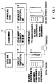
- an information processing apparatus to which an extended memory address control system according to an embodiment of the present invention is applied comprises a system controller 1, an I/O processor 2, connected thereto, for controlling system I/Os, a control processor 3 having program compiling and linking functions, and a supervisor function, a high-speed arithmetic processor 4 for executing a user program mainly consisting of vector calculations at high speed, a control main memory 5 which serves as a memory for the control processor 3 and on which an operating system function can be operated, a large-capacity, high-speed arithmetic main memory 6 which is used for the high-speed arithmetic processor 4 and stores vector data of user programs mainly consisting of vector calculations and user programs executed by the high-speed arithmetic processor 4, and an extended memory 7.
- the system controller 1 includes an extended memory data transfer control unit 9 for controlling data transfer between the extended memory 7 and the control main memory 5 on the basis of commands on the high-speed arithmetic processor 4 in accordance with a data transfer request between the extended memory 7 and the arithmetic main memory 6 from a processor included in a first processor group including the control processor 3, the I/O processor and the like, and a monitor call request of a user program executed on the high-speed arithmetic processor 4, and for controlling data transfer between the extended memory 7 and the control main memory 5 in accordance with a data transfer request between the extended memory 7 and the control main memory 5, which is issued from a processor included in the first processor group.
- an extended memory data transfer control unit 9 for controlling data transfer between the extended memory 7 and the control main memory 5 on the basis of commands on the high-speed arithmetic processor 4 in accordance with a data transfer request between the extended memory 7 and the arithmetic main memory 6 from a processor included in a first processor group including the control processor 3, the I/O
- the control processor 3 has a disk address designation means 20 for managing the extended memory 7 as a virtual disk, a memory address designation means 21 for managing the extended memory 7 as a continuous memory space, and a memory address conversion means 25 for converting memory addresses designated by the memory address designation means 21 to physical addresses of the extended memory 7.
- the high-speed arithmetic processor 4 has a disk address conversion means 23 for converting virtual disk addresses designated by the disk address designation means 20 to physical addresses of the extended memory 7, a memory address conversion means 24 for converting memory addresses designated by the memory address designation means 21 to physical addresses of the extended memory 7, and a type discrimination means 22 for discriminating whether the extended memory 7 is managed as the virtual disk or the continuous memory space.
- the control processor 3 has supervisor functions such as job I/O edit processing, file processing, resource management for the I/O processor 2, job scheduling, a compiler and a linker for user programs, and the like.
- the high-speed arithmetic processor 4 has a function of being able to execute vector or scalar commands of a user program at high speed, and employs a multiple parallel pipeline system for executing vector calculations especially at high speed.
- the high-speed arithmetic processor 4 is controlled by an arithmetic data transfer control unit 8 to increase a throughput between the high-speed arithmetic processor 4 and the arithmetic main memory 6.
- Data transfer between the extended memory 7 and the arithmetic main memory 6 is controlled by commands on the high-speed arithmetic processor 4. Therefore, while transfer is executed between the extended memory 7 and the arithmetic main memory 6, high-speed execution processing of vector or scalar commands of a user program executed on the high-speed arithmetic processor 4 is interrupted.
- an address type Pa and an extended memory address Pb are stored on the channel program CP by the disk address designation means 20 or the memory address designation means 21 in accordance with a format of addresses in the extended memory 7 to be processed by an operating system.
- the channel program CP also includes control information such as an arithmetic main memory address Pc, a transfer length Pd, and the like.
- the transfer command is executed as an asynchronous command on the control processor 3. For example, if a certain process includes n transfer commands, n channel programs (CP 1 ,..., CP n ) corresponding to these commands are created, as shown in Fig. 3.
- the control processor 3 executes interprocessor communication with the high-speed arithmetic processor 4 after it creates all the channel programs.
- the high-speed arithmetic processor 4 Upon reception of the interprocessor communication command, the high-speed arithmetic processor 4 reads out channel program information created in the arithmetic main memory 6 by the control processor 3. Thereafter, the type discrimination means 22 discriminates whether the extended memory 7 is managed as a virtual disk or a continuous memory space. According to a discrimination result, the extended memory address is converted to the physical address using the disk address conversion means 23 or the memory address conversion means 24.
- the high-speed arithmetic processor 4 executes an extended memory data transfer command, and sends control information such as a type of command, the converted physical address of the extended memory 7, the start address of the arithmetic main memory 6, and the like, thus starting data transfer between the arithmetic main memory 6 and the extended memory 7.
- the extended memory data transfer control unit 9 sequentially reads data from the arithmetic main memory 6, and transfers them to the extended memory 7.
- the high-speed arithmetic processor which received the data transfer completion message reads status to discriminate normality/abnormality of data transfer, and reports the discrimination result to the control processor 3 through the interprocessor communication.
- the memory address conversion means, the disk address conversion means, and the type discrimination means may be arranged in the system controller 1 in accordance with a hardware volume/performance depending on a system configuration.
- Data transfer between the extended memory 7 and the control main memory 5 is processed by an operating system of only a continuous memory address format.
- control processor 3 causes the memory address conversion means 25 to convert a designated address of the extended memory 7 to a physical address using a memory address conversion means 25.
- the control processor 3 then sends the start address of the control main memory 5, the start address of the extended memory 7, commands, a transfer data volume, and the like to the extended memory data transfer control unit 9, thus starting data transfer.
- a message indicating this is supplied from the extended memory data transfer control unit 9 to the control processor 3.
- the control processor 3 reads status to discriminate normality/abnormality of data transfer.
- whether the extended memory is managed as a continuous memory address space or a virtual disk address space is designated under the control of an operating system, so that an overhead of managing address spaces can be reduced, as needed, to improve access performance.
- addresses of the extended memory are processed as virtual disk addresses.
- a user can unconsciously execute such a program under the control of an operating system without modifying the program.
Landscapes
- Engineering & Computer Science (AREA)
- Theoretical Computer Science (AREA)
- Physics & Mathematics (AREA)
- General Engineering & Computer Science (AREA)
- General Physics & Mathematics (AREA)
- Human Computer Interaction (AREA)
- Memory System Of A Hierarchy Structure (AREA)
- Memory System (AREA)
- Information Retrieval, Db Structures And Fs Structures Therefor (AREA)
Claims (1)
- Système de commande d'adresses pour mémoire étendue dans un dispositif de traitement d'informations comportant une unité de commande de système (1), un processeur arithmétique haute-vitesse (4), une première mémoire principale, et une mémoire étendue (7), caractérisé en ce qu'il comporte en outre un processeur de commande (3), dans un premier groupe de processeurs, qui a une fonction de supervision, et réalise une commande d'entrée/sortie, et un compilateur et un éditeur de liens destinés à un programme-utilisateur, et une seconde mémoire principale (6) pour mémoriser un module de chargement du programme-utilisateur, ainsi que des données, ladite première mémoire principale (5) étant fournie pour mémoriser un programme de commande destiné à commander ledit processeur de commande (3), ledit processeur arithmétique haute-vitesse (4) se trouvant dans un second groupe de processeurs destinés à exécuter le programme-utilisateur, ladite mémoire étendue (7) étant fournie pour augmenter la vitesse d'entrée/sortie, et ladite unité de commande de système (1) étant fournie pour commander ledit processeur de commande (3), ladite première mémoire principale (5), ladite seconde mémoire principale (6), ledit processeur arithmétique haute-vitesse (4), et une mémoire étendue (7), ledit système de commande d'adresses pour mémoire étendue comportant :dans lequel le transfert de données entre ladite première mémoire principale (5) et ladite mémoire étendue (7), exécuté par ledit processeur de commande (3), est exécuté en ne commandant les adresses que par l'intermédiaire des moyens de désignation d'adresse de mémoire (21), et le transfert de données entre ladite seconde mémoire principale (6) et ladite mémoire étendue (7), exécuté par ledit processeur arithmétique haute-vitesse (4), est exécuté en commandant les adresses par l'intermédiaire desdits moyens de désignation d'adresse de disque (20) et desdits moyens de désignation d'adresse de mémoire (21).des moyens de désignation d'adresse de disque (20) pour gérer ladite mémoire étendue (7) comme s'il s'agissait d'un disque virtuel,des moyens de conversion d'adresse de disque (23) pour convertir une adresse de disque virtuel, désignée par lesdits moyens de désignation d'adresse de disque (20), en une première adresse physique de ladite mémoire étendue (7),des moyens de désignation d'adresse de mémoire (21) pour gérer ladite mémoire étendue (7) comme s'il s'agissait d'un espace-mémoire continu,des moyens de conversion d'adresse de mémoire (24, 25) pour convertir une adresse de mémoire, désignée par lesdits moyens de désignation d'adresse de mémoire (21), en une seconde adresse physique de ladite mémoire étendue (7),des moyens de discrimination de type (22) pour déterminer si ladite mémoire étendue (7) est gérée comme s'il s'agissait d'un disque virtuel ou d'un espace-mémoire continu, etdes moyens de commande d'accès pour accéder à ladite mémoire étendue (7) en utilisant l'une parmi les première et seconde adresses physiques en fonction d'une indication fournie par lesdits moyens de discrimination de type (22),
Applications Claiming Priority (2)
| Application Number | Priority Date | Filing Date | Title |
|---|---|---|---|
| JP62264/89 | 1989-03-16 | ||
| JP1062264A JP2513024B2 (ja) | 1989-03-16 | 1989-03-16 | 拡張記憶アドレス制御方式 |
Publications (3)
| Publication Number | Publication Date |
|---|---|
| EP0387871A2 EP0387871A2 (fr) | 1990-09-19 |
| EP0387871A3 EP0387871A3 (fr) | 1991-06-05 |
| EP0387871B1 true EP0387871B1 (fr) | 1998-10-07 |
Family
ID=13195117
Family Applications (1)
| Application Number | Title | Priority Date | Filing Date |
|---|---|---|---|
| EP90104907A Expired - Lifetime EP0387871B1 (fr) | 1989-03-16 | 1990-03-15 | Système de commande d'adresse pour mémoire étendue |
Country Status (6)
| Country | Link |
|---|---|
| US (1) | US5404477A (fr) |
| EP (1) | EP0387871B1 (fr) |
| JP (1) | JP2513024B2 (fr) |
| AU (1) | AU621723B2 (fr) |
| CA (1) | CA2012420C (fr) |
| DE (1) | DE69032688T2 (fr) |
Cited By (1)
| Publication number | Priority date | Publication date | Assignee | Title |
|---|---|---|---|---|
| CN101800811B (zh) * | 2010-02-02 | 2012-10-03 | 中国软件与技术服务股份有限公司 | 手机数据安全防护方法 |
Families Citing this family (19)
| Publication number | Priority date | Publication date | Assignee | Title |
|---|---|---|---|---|
| FR2669132A1 (fr) * | 1990-11-09 | 1992-05-15 | Guerin James | Dispositif de memorisation d'informations connectable a un ordinateur. |
| US5420998A (en) * | 1992-04-10 | 1995-05-30 | Fujitsu Limited | Dual memory disk drive |
| JPH0778766B2 (ja) * | 1992-09-25 | 1995-08-23 | インターナショナル・ビジネス・マシーンズ・コーポレイション | ランダム・アクセス可能かつ書換え可能メモリを用いる外部記憶装置におけるプログラム直接実行の制御方法および装置 |
| JP3564732B2 (ja) * | 1994-06-30 | 2004-09-15 | ソニー株式会社 | ディスク制御方法および装置 |
| US6356915B1 (en) | 1999-02-22 | 2002-03-12 | Starbase Corp. | Installable file system having virtual file system drive, virtual device driver, and virtual disks |
| JP2001034537A (ja) * | 1999-07-23 | 2001-02-09 | Toshiba Corp | アドレス変換回路 |
| US6833926B1 (en) * | 1999-09-28 | 2004-12-21 | Kabushiki Kaisha Toshiba | Image processing apparatus |
| WO2001044967A1 (fr) * | 1999-12-14 | 2001-06-21 | Fujitsu Limited | Systeme multiprocesseur |
| US6490651B1 (en) * | 2000-03-14 | 2002-12-03 | Maxtor Corporation | Host-based virtual disk drive for improving the performance of a hard disk drive's input/output |
| US6981125B2 (en) * | 2003-04-22 | 2005-12-27 | International Business Machines Corporation | Method and apparatus for managing shared virtual storage in an information handling system |
| US20070055819A1 (en) * | 2003-11-07 | 2007-03-08 | Hirokazu So | Information recording medium and its control method |
| US7222117B1 (en) | 2003-11-14 | 2007-05-22 | Advent Software, Inc. | Segmented global area database |
| CN100464315C (zh) * | 2006-05-22 | 2009-02-25 | 中国软件与技术服务股份有限公司 | 移动存储器失泄密防护的方法和系统 |
| US8458217B1 (en) | 2009-08-24 | 2013-06-04 | Advent Software, Inc. | Instantly built information space (IBIS) |
| US8769350B1 (en) | 2011-09-20 | 2014-07-01 | Advent Software, Inc. | Multi-writer in-memory non-copying database (MIND) system and method |
| US8332349B1 (en) | 2012-01-06 | 2012-12-11 | Advent Software, Inc. | Asynchronous acid event-driven data processing using audit trail tools for transaction systems |
| CN102946427A (zh) * | 2012-11-07 | 2013-02-27 | 浪潮电子信息产业股份有限公司 | 一种存储系统的新型注册方法 |
| US8886671B1 (en) | 2013-08-14 | 2014-11-11 | Advent Software, Inc. | Multi-tenant in-memory database (MUTED) system and method |
| CN110059020B (zh) * | 2015-04-23 | 2024-01-30 | 华为技术有限公司 | 扩展内存的访问方法、设备以及系统 |
Family Cites Families (8)
| Publication number | Priority date | Publication date | Assignee | Title |
|---|---|---|---|---|
| US5012407A (en) * | 1984-12-11 | 1991-04-30 | Finn Charles A | Computer system which accesses operating system information and command handlers from optical storage via an auxiliary processor and cache memory |
| US4761733A (en) * | 1985-03-11 | 1988-08-02 | Celerity Computing | Direct-execution microprogrammable microprocessor system |
| US4758951A (en) * | 1985-04-09 | 1988-07-19 | Tektronix, Inc. | Method for translating virtual addresses into real addresses |
| JPS6261132A (ja) * | 1985-09-12 | 1987-03-17 | Fujitsu Ltd | デ−タ転送命令制御方式 |
| US4926322A (en) * | 1987-08-03 | 1990-05-15 | Compag Computer Corporation | Software emulation of bank-switched memory using a virtual DOS monitor and paged memory management |
| US5127094A (en) * | 1987-11-09 | 1992-06-30 | Hitachi, Ltd. | Virtual storage type computer system |
| US5129088A (en) * | 1987-11-30 | 1992-07-07 | International Business Machines Corporation | Data processing method to create virtual disks from non-contiguous groups of logically contiguous addressable blocks of direct access storage device |
| US5131089A (en) * | 1989-06-12 | 1992-07-14 | Grid Systems Corporation | Solid state disk drive emulation |
-
1989
- 1989-03-16 JP JP1062264A patent/JP2513024B2/ja not_active Expired - Lifetime
-
1990
- 1990-03-15 EP EP90104907A patent/EP0387871B1/fr not_active Expired - Lifetime
- 1990-03-15 DE DE69032688T patent/DE69032688T2/de not_active Expired - Fee Related
- 1990-03-16 AU AU51398/90A patent/AU621723B2/en not_active Ceased
- 1990-03-16 CA CA002012420A patent/CA2012420C/fr not_active Expired - Fee Related
-
1993
- 1993-10-05 US US08/131,876 patent/US5404477A/en not_active Expired - Fee Related
Cited By (1)
| Publication number | Priority date | Publication date | Assignee | Title |
|---|---|---|---|---|
| CN101800811B (zh) * | 2010-02-02 | 2012-10-03 | 中国软件与技术服务股份有限公司 | 手机数据安全防护方法 |
Also Published As
| Publication number | Publication date |
|---|---|
| DE69032688T2 (de) | 1999-02-25 |
| CA2012420A1 (fr) | 1990-09-16 |
| DE69032688D1 (de) | 1998-11-12 |
| EP0387871A3 (fr) | 1991-06-05 |
| US5404477A (en) | 1995-04-04 |
| JPH02242451A (ja) | 1990-09-26 |
| JP2513024B2 (ja) | 1996-07-03 |
| CA2012420C (fr) | 1996-03-26 |
| EP0387871A2 (fr) | 1990-09-19 |
| AU5139890A (en) | 1990-09-20 |
| AU621723B2 (en) | 1992-03-19 |
Similar Documents
| Publication | Publication Date | Title |
|---|---|---|
| EP0387871B1 (fr) | Système de commande d'adresse pour mémoire étendue | |
| US4860190A (en) | Computer system for controlling virtual machines | |
| US5278973A (en) | Dual operating system computer | |
| US5530845A (en) | Storage control subsystem implemented with an application program on a computer | |
| US4365292A (en) | Array processor architecture connection network | |
| US5109489A (en) | I/o execution method for a virtual machine system and system therefor | |
| GB2024476A (en) | Dynamic disc buffer control unit | |
| US5796989A (en) | Method and system for increasing cache efficiency during emulation through operation code organization | |
| US5935219A (en) | Message handling in data processing apparatus | |
| JPS60176143A (ja) | プログラム呼び出し装置 | |
| JP2003296191A (ja) | 汎用プロセッサおよび周辺装置のプロセッサとして動作可能な集積回路 | |
| EP0139254A2 (fr) | Appareil et méthode pour un transfert direct de données de mémoire vers un dispositif périphérique et du dispositif périphérique vers la mémoire | |
| US4791560A (en) | Macro level control of an activity switch in a scientific vector processor which processor requires an external executive control program | |
| EP0442297B1 (fr) | Processeur à mémoire de microcode réinscriptible | |
| JP2527038B2 (ja) | 拡張記憶転送制御方式 | |
| EP0297892A2 (fr) | Dispositif et méthode pour commander des événements d'interruptions asynchrones de programme dans un système de traitement de données | |
| JPH04149658A (ja) | 情報処理装置 | |
| WO1991004535A1 (fr) | Module de memoire pour un systeme informatique a gestion de memoire | |
| JPH09282196A (ja) | 複合論理プロセッサシステムのプログラム走行制御方式 | |
| KR880001399B1 (ko) | 정보 처리 장치 | |
| JPH03188530A (ja) | プログラム先取り装置 | |
| EP0319280A2 (fr) | Dispositif et système de traitement réparti à structure hiérarchique | |
| JPH02113339A (ja) | 仮想計算機制御方式 | |
| JPS6091452A (ja) | デ−タ処理装置のタスクスケジユ−リング方式 | |
| Weaver et al. | Operating system considerations in the multiprocessor MIDAS environment |
Legal Events
| Date | Code | Title | Description |
|---|---|---|---|
| PUAI | Public reference made under article 153(3) epc to a published international application that has entered the european phase |
Free format text: ORIGINAL CODE: 0009012 |
|
| 17P | Request for examination filed |
Effective date: 19900411 |
|
| AK | Designated contracting states |
Kind code of ref document: A2 Designated state(s): BE DE FR GB IT NL |
|
| PUAL | Search report despatched |
Free format text: ORIGINAL CODE: 0009013 |
|
| AK | Designated contracting states |
Kind code of ref document: A3 Designated state(s): BE DE FR GB IT NL |
|
| 17Q | First examination report despatched |
Effective date: 19941227 |
|
| GRAG | Despatch of communication of intention to grant |
Free format text: ORIGINAL CODE: EPIDOS AGRA |
|
| GRAG | Despatch of communication of intention to grant |
Free format text: ORIGINAL CODE: EPIDOS AGRA |
|
| GRAH | Despatch of communication of intention to grant a patent |
Free format text: ORIGINAL CODE: EPIDOS IGRA |
|
| GRAH | Despatch of communication of intention to grant a patent |
Free format text: ORIGINAL CODE: EPIDOS IGRA |
|
| GRAA | (expected) grant |
Free format text: ORIGINAL CODE: 0009210 |
|
| AK | Designated contracting states |
Kind code of ref document: B1 Designated state(s): BE DE FR GB IT NL |
|
| REF | Corresponds to: |
Ref document number: 69032688 Country of ref document: DE Date of ref document: 19981112 |
|
| ET | Fr: translation filed | ||
| PGFP | Annual fee paid to national office [announced via postgrant information from national office to epo] |
Ref country code: BE Payment date: 19990205 Year of fee payment: 10 |
|
| PGFP | Annual fee paid to national office [announced via postgrant information from national office to epo] |
Ref country code: GB Payment date: 19990318 Year of fee payment: 10 |
|
| PGFP | Annual fee paid to national office [announced via postgrant information from national office to epo] |
Ref country code: NL Payment date: 19990331 Year of fee payment: 10 |
|
| PGFP | Annual fee paid to national office [announced via postgrant information from national office to epo] |
Ref country code: FR Payment date: 19990427 Year of fee payment: 10 |
|
| PGFP | Annual fee paid to national office [announced via postgrant information from national office to epo] |
Ref country code: DE Payment date: 19990528 Year of fee payment: 10 |
|
| PLBE | No opposition filed within time limit |
Free format text: ORIGINAL CODE: 0009261 |
|
| STAA | Information on the status of an ep patent application or granted ep patent |
Free format text: STATUS: NO OPPOSITION FILED WITHIN TIME LIMIT |
|
| 26N | No opposition filed | ||
| PG25 | Lapsed in a contracting state [announced via postgrant information from national office to epo] |
Ref country code: GB Free format text: LAPSE BECAUSE OF NON-PAYMENT OF DUE FEES Effective date: 20000315 |
|
| PG25 | Lapsed in a contracting state [announced via postgrant information from national office to epo] |
Ref country code: BE Free format text: LAPSE BECAUSE OF NON-PAYMENT OF DUE FEES Effective date: 20000331 |
|
| BERE | Be: lapsed |
Owner name: NEC CORP. Effective date: 20000331 |
|
| PG25 | Lapsed in a contracting state [announced via postgrant information from national office to epo] |
Ref country code: NL Free format text: LAPSE BECAUSE OF NON-PAYMENT OF DUE FEES Effective date: 20001001 |
|
| GBPC | Gb: european patent ceased through non-payment of renewal fee |
Effective date: 20000315 |
|
| PG25 | Lapsed in a contracting state [announced via postgrant information from national office to epo] |
Ref country code: FR Free format text: LAPSE BECAUSE OF NON-PAYMENT OF DUE FEES Effective date: 20001130 |
|
| NLV4 | Nl: lapsed or anulled due to non-payment of the annual fee |
Effective date: 20001001 |
|
| REG | Reference to a national code |
Ref country code: FR Ref legal event code: ST |
|
| PG25 | Lapsed in a contracting state [announced via postgrant information from national office to epo] |
Ref country code: DE Free format text: LAPSE BECAUSE OF NON-PAYMENT OF DUE FEES Effective date: 20010103 |
|
| PG25 | Lapsed in a contracting state [announced via postgrant information from national office to epo] |
Ref country code: IT Free format text: LAPSE BECAUSE OF NON-PAYMENT OF DUE FEES;WARNING: LAPSES OF ITALIAN PATENTS WITH EFFECTIVE DATE BEFORE 2007 MAY HAVE OCCURRED AT ANY TIME BEFORE 2007. THE CORRECT EFFECTIVE DATE MAY BE DIFFERENT FROM THE ONE RECORDED. Effective date: 20050315 |