EP0386727A1 - Method for producing single crystal diamond film - Google Patents
Method for producing single crystal diamond film Download PDFInfo
- Publication number
- EP0386727A1 EP0386727A1 EP90104346A EP90104346A EP0386727A1 EP 0386727 A1 EP0386727 A1 EP 0386727A1 EP 90104346 A EP90104346 A EP 90104346A EP 90104346 A EP90104346 A EP 90104346A EP 0386727 A1 EP0386727 A1 EP 0386727A1
- Authority
- EP
- European Patent Office
- Prior art keywords
- single crystal
- diamond film
- containing compound
- oxygen
- carbon
- Prior art date
- Legal status (The legal status is an assumption and is not a legal conclusion. Google has not performed a legal analysis and makes no representation as to the accuracy of the status listed.)
- Granted
Links
Images

Classifications
-
- C—CHEMISTRY; METALLURGY
- C30—CRYSTAL GROWTH
- C30B—SINGLE-CRYSTAL GROWTH; UNIDIRECTIONAL SOLIDIFICATION OF EUTECTIC MATERIAL OR UNIDIRECTIONAL DEMIXING OF EUTECTOID MATERIAL; REFINING BY ZONE-MELTING OF MATERIAL; PRODUCTION OF A HOMOGENEOUS POLYCRYSTALLINE MATERIAL WITH DEFINED STRUCTURE; SINGLE CRYSTALS OR HOMOGENEOUS POLYCRYSTALLINE MATERIAL WITH DEFINED STRUCTURE; AFTER-TREATMENT OF SINGLE CRYSTALS OR A HOMOGENEOUS POLYCRYSTALLINE MATERIAL WITH DEFINED STRUCTURE; APPARATUS THEREFOR
- C30B25/00—Single-crystal growth by chemical reaction of reactive gases, e.g. chemical vapour-deposition growth
- C30B25/02—Epitaxial-layer growth
-
- C—CHEMISTRY; METALLURGY
- C30—CRYSTAL GROWTH
- C30B—SINGLE-CRYSTAL GROWTH; UNIDIRECTIONAL SOLIDIFICATION OF EUTECTIC MATERIAL OR UNIDIRECTIONAL DEMIXING OF EUTECTOID MATERIAL; REFINING BY ZONE-MELTING OF MATERIAL; PRODUCTION OF A HOMOGENEOUS POLYCRYSTALLINE MATERIAL WITH DEFINED STRUCTURE; SINGLE CRYSTALS OR HOMOGENEOUS POLYCRYSTALLINE MATERIAL WITH DEFINED STRUCTURE; AFTER-TREATMENT OF SINGLE CRYSTALS OR A HOMOGENEOUS POLYCRYSTALLINE MATERIAL WITH DEFINED STRUCTURE; APPARATUS THEREFOR
- C30B29/00—Single crystals or homogeneous polycrystalline material with defined structure characterised by the material or by their shape
- C30B29/02—Elements
- C30B29/04—Diamond
-
- Y—GENERAL TAGGING OF NEW TECHNOLOGICAL DEVELOPMENTS; GENERAL TAGGING OF CROSS-SECTIONAL TECHNOLOGIES SPANNING OVER SEVERAL SECTIONS OF THE IPC; TECHNICAL SUBJECTS COVERED BY FORMER USPC CROSS-REFERENCE ART COLLECTIONS [XRACs] AND DIGESTS
- Y10—TECHNICAL SUBJECTS COVERED BY FORMER USPC
- Y10S—TECHNICAL SUBJECTS COVERED BY FORMER USPC CROSS-REFERENCE ART COLLECTIONS [XRACs] AND DIGESTS
- Y10S117/00—Single-crystal, oriented-crystal, and epitaxy growth processes; non-coating apparatus therefor
- Y10S117/918—Single-crystal waveguide
- Y10S117/919—Organic
Definitions
- the present invention relates to a method for producing a single crystal diamond film.
- the present invention relates to a method for producing a single crystal diamond film having good crystallinity, a smooth surface, and good electrical and optical characteristics.
- Diamond has a large forbidden band width, a large electron mobility, a large hole mobility, a large saturation electron mobility, a large thermal conductivity, a low dielectric constant and high clarity. Therefore, the diamond is highly expected as a material for semiconductors, for example, semiconductive elements having heat resistance and radiation resistance and high speed high output semiconductive elements, and as an element for emitting blue light or UV light.
- R. Mania et al proposed a method for synthesizing diamond in a vapor phase which comprises decomposing and exciting a raw material comprising a hydrocarbon gas such as methane with radiofrequency discharge (R. Mania et al, Crystal Research and Technology, 16 , 785 (1981)).
- the semiconductor field requires not only a diamond single crystal having high purity and crystallinity, but also one that has good crystallinity and contains a suitable amount of a certain impurity (dopant) with which valence electrons can be controlled.
- the single crystal diamond film can be grown on a diamond single crystal which has been synthesized under ultra-high pressure and that when the single crystal diamond is doped with an impurity such as boron acts as a p-type semiconductor (N. Fujimonri et al, Vacuum, 36 , 99 (1986)).
- the impurity is doped by a conventional method for growing a single crystal diamond film by using a hydrocarbon gas and a hydrogen gas, a surface in, for example, the (110) plane has large irregularity so that the diamond crystal abnormally grows on the (110) plane.
- the electrical characteristics of the semiconductive element when a Schottky diode is fabricated, it has a large reverse direction leak current.
- An object of the present invention is to provide a method for producing a single crystal diamond film having a smooth surface, good crystallinity, and improved electrical characteristics.
- the present invention provides a method for producing a single crystal diamond film, which comprises steps of decomposing a raw material gas comprising a hydrogen gas, a carbon-containing compound and an oxygen- containing compound and growing a single crystal diamond film on a substrate in a vapor phase.
- the method of the present invention is particularly useful when the raw material contains a dopant.
- the raw material to be used according to the present invention comprises a hydrogen gas, a carbon-containing compound, an oxygen-containing compound and optionally a dopant and is supplied to a reaction chamber in a vapor phase.
- the raw material is preferably diluted with an inert gas.
- the carbon-containing compound examples include paraffinic hydrocarbons (e.g. methane, ethane, propane, butane, etc.), olefinic hydrocarbons (e.g. ethylene, propylene, butylene, etc.), acetylene type hydrocarbons (e.g. acetylene, allylene, etc.), dienes (e.g. butadiene, etc.), alicyclic hydrocarbons (e.g. cyclopropane, cyclobutane, cyclopentane, cyclohexane, etc.), aromatic hydrocarbons (e.g.
- paraffinic hydrocarbons e.g. methane, ethane, propane, butane, etc.
- olefinic hydrocarbons e.g. ethylene, propylene, butylene, etc.
- acetylene type hydrocarbons e.g. acetylene, allylene
- the carbon-containing compound may be a compound consisting of carbon atoms such as graphite, coal and coke.
- oxygen-containing compound oxygen, water, carbon monoxide, carbon dioxide and hydrogen peroxide are preferable since they are easily available.
- carbon monoxide or carbon dioxide When carbon monoxide or carbon dioxide is used, other carbon-containing compound is not necessarily used.
- the inert gas includes argon, helium, neon, krypton, xenon and radon.
- elemental boron lithium, nitrogen, phosphorus, sulfur, chlorine, arsenic or selenium and their compounds can be used.
- the moles of the hydrogen gas (A), the inert gas (B), the carbon atoms contained in the carbon-containing compound (C) and the oxygen atoms contained in the oxygen-containing compound (D) preferably satisfy the following equations: 0.02 ⁇ C/(A+B+C+D) ⁇ 0.5 and 0.01 ⁇ D/C ⁇ 1.
- the ratio: C/(A+B+C+D) is less than 0.02, the surface of the diamond film tends to lose its smoothness. When this ratio is 0.5 or larger, the graphite component tends to deposit.
- the ratio: D/C is less than 0.01, the crystallinity of the diamond film tends to decrease.
- this ratio is larger than 1 (one), the formation of the diamond film may be inhibited.
- a lattice constant (a) of which satisfies the following relation can be used:
- x 100 ⁇ 20 in which a0 is the lattice constant of the single crystal diamond ( 3.567 ⁇ ) and a is a lattice constant of the substrate.
- Examples of such substrate material are magnesium oxide (a: 4.213 ⁇ ), Ni (a: 3.524 ⁇ ), Cu (a: 3.6147 ⁇ ), Ni/Cu alloy, ⁇ -SiC (a: 4.36 ⁇ ), ⁇ -SiC (a: 3.0807 ⁇ ), C-BN (a: 3.615 ⁇ ), AlN (a: 3.104 ⁇ ), PbTiO3 (a: 3.90 ⁇ ), Ba2TiO4 (a: 3.994 ⁇ ), GaN (a: 3.180 ⁇ ), ZnO (a: 3.2407 ⁇ ), ZnS (a: 3.820 ⁇ ), ZrO2 (a: 3.64 ⁇ ), oxide superconductive materials such as Tl2Ba2Ca2Cu3O10 (a: 3.85 ⁇ ) or Y1Ba2CU3O 7-x (a: 3.89 ⁇ ) and the like.
- the vapor deposition of diamond can be carried out by a conventional method such as microwave plasma CVD (chemical vapor deposition), thermal filament CVD, RF plasma CVD, DC plasma CVD, plasma jet, chemical transportation, and the like.
- a conventional method such as microwave plasma CVD (chemical vapor deposition), thermal filament CVD, RF plasma CVD, DC plasma CVD, plasma jet, chemical transportation, and the like.
- the plasma CVD using alternating current of 1KHz or larger, particularly microwave plasma CVD is preferred, since the deposited diamond is less contaminated with impurities from a reaction chamber.
- the pressure in the reaction chamber is usually from 10 ⁇ 4 to 103 Torr.
- the temperature of the substrate depends on the kind of substrate. Preferably, it is from 700 to 1000°C.
- the diamond is epitaxially grown in a state in which a degree of supersaturation of the carbon-containing compound in the vapor phase is large and which is close to the thermodynamic equilibrium.
- the graphite component contaminates the deposited diamond film or deposits in the reaction chamber to change the process conditions, although the film smoothness of the deposited diamond is improved.
- the oxygen-containing compound is added to the carbon-containing compound, the former is decomposed to generate oxygen radicals or hydroxyl radicals. These radicals accelerate the decomposition of the carbon-containing compound and react selectively with the by-produced graphite to remove it.
- the addition of the oxygen-containing compound makes it possible to synthesize the single crystal diamond film in the supersaturated state of the carbon-containing compound in the vapor phase, whereby the single crystal diamond having the smooth surface and good electrical and optical characteristics can be produced.
- Fig. 1 schematically shows a preferred embodiment of an apparatus for carrying out the method of the present invention.
- Hydrogen gas 1, methane gas 2 as the carbon-containing compound and diborane gas 3 are metered with respective mass flowmeters 5, mixed and then supplied in a reaction chamber 6.
- Oxygen gas 5 as the oxygen-containing compound is metered with a mass flowmeter 5 and then supplied in the reaction chamber 6 through a supply line different from one for supplying the above mixture since the oxygen gas reacts with diborane.
- the gas mixture is decomposed in the chamber 6 with microwave 7.
- Carbon atoms generated through decomposition of methane is heated to several hundred degree (°C) and reaches a single crystal diamond substrate 8 to form a diamond layer and a graphite layer.
- the graphite layer is removed through reaction of carbon with hydrogen atoms generated by the decomposition of hydrogen or oxygen atoms generated by the decomposition of oxygen.
- the reaction chamber 6 is evacuated
- Fig. 2 is a cross section of a device for supplying a liquid material such as water and methanol to the reaction chamber in a vapor state.
- the hydrogen gas 11 is metered with the mass flow meter 12 and flowed through a liquid material 14 contained in a glass vessel 13.
- the liquid material 14 is entrained with the hydrogen gas flow and supplied in the reaction chamber.
- the vessel 13 can be heated with a heater 15.
- a single crystal diamond film was grown by using the apparatus of Fig. 1.
- the reaction chamber was made of quartz and had an inner diameter of 44 mm and a length of 600 mm.
- a diamond single crystal of 1.5 mm in length, 2.0 mm in width and 0.3 mm in thickness was used with the (100) plane forming a deposition surface.
- a mixture of methane, hydrogen, diborane and oxygen in a molar ratio of Table 1 (Example 1) or a mixture of methane, hydrogen and diborane in a molar ratio of Table 1 (Comparative Examples 1 and 2) was used as the raw material.
- the total flow rate of the raw material was 100 sccm.
- Comparative Example 1 Although the good quality diamond film containing no graphite component was produced, the surface roughness was about 2000 ⁇ . When the amount of methane was increased as in Comparative Example 2, although the diamond film having surface roughness of less than 100 ⁇ was produced, the presence of the amorphous component was confirmed by electron diffraction analysis.
- Example 1 the diamond film had surface roughness of less than 100 ⁇ and the electron diffraction gave a streak pattern which indicates a single crystal having uniformity in the atomic level.
- Electrodes were formed on the obtained diamond film to assemble a Schottky diode.
- the characteristics of the diode were evaluated from a forward direction current If and a reverse direction leak current Ir in the diode.
- Example 2 With the diode which was fabricated from the diamond film obtained in Example 1, an amount of Ir was less than one thousandth of If, and good rectification was achieved.
- the diode characteristics in Example 1 is shown in Fig. 5.
- Example No. 1 Comp. 1
- ⁇ Surface roughness ( ⁇ ) ⁇ 100 ca. 2000 ⁇ 100 Crystallinity Complete single crystal Partly crystallized Partly amorphous Electron diffraction pattern Streak patter Streak pattern + ring patter Halo pattern Diode characteristics Ir ⁇ If/1000 see Fig. 5 Ir ⁇ If/10 see Fig. 3 Ir ⁇ If/10 see Fig. 4
- Example 2 In the same manner as in Example 1 but supplying hydrogen gas at 100 sccm, methane at 10 sccm, diborane (diluted with hydrogen to 10 ppm) at 10 sccm and carbon dioxide at 2 sccm in the reaction chamber and reacting them at a substrate temperature of 830°C under pressure of 40 Torr for 2 hours to deposit a diamond film of 1.2 ⁇ m in thickness.
- the diamond film was a single crystal with good crystallinity and surface roughness of less than 100 ⁇ , and had high hole mobility of about 1000 cm2/V.sec.
- a Schottky diode fabricated from this diamond film achieved good rectification.
- the diamond film contained a graphite component and had neither good crystallinity nor electrical characteristics.
- Example 2 In the same manner as in Example 1 but supplying hydrogen gas at 100 sccm, methane at 10 sccm, diborane (diluted with hydrogen to 10 ppm) at 10 sccm and carbon monoxide at 3 sccm in the reaction chamber and reacting them at a substrate temperature of 830°C under pressure of 40 Torr for 2 hours to deposit a diamond film of 1.5 ⁇ m in thickness.
- the diamond film was a single crystal with good crystallinity and surface roughness of less than 100 ⁇ , and had high hole mobility of about 1000 cm2/V.sec.
- a Schottky diode fabricated from this diamond film achieved good rectification.
- the diamond film contained a graphite component and had neither good crystallinity nor electrical characteristics.
- Example 2 In the same manner as in Example 1 but supplying hydrogen gas at 100 sccm, argon at 50 sccm, methane at 15 sccm, diborane (diluted with hydrogen to 10 ppm) at 10 sccm and oxygen at 2 sccm in the reaction chamber and reacting them at a substrate temperature of 850°C under pressure of 80 Torr for 2 hours to deposit a diamond film of 2 ⁇ m in thickness.
- the diamond film was a single crystal with good crystallinity and surface roughness of less than 100 ⁇ , and had high hole mobility of about 1000 cm2/V.sec.
- a Schottky diode fabricated from this diamond film achieved good rectification.
- the diamond film contained a graphite component and had neither good crystallinity nor electrical characteristics.
- the diamond with good quality can be epitaxially grown at a growth rate at least twice larger than in case of the absence of the inert gas.
- Example 2 In the same manner as in Example 1 but supplying hydrogen gas at 100 sccm in total, methane at 10 sccm, diborane (diluted with hydrogen to 10 ppm) at 10 sccm and water at 2 sccm (as converted to a saturated vapor pressure) in the reaction chamber and reacting them at a substrate temperature of 830°C under pressure of 40 Torr for 2 hours to deposit a diamond film of 1.1 ⁇ m in thickness. To supply water, the device of Fig. 2 was used. The diamond film was a single crystal with good crystallinity and surface roughness of less than 100 ⁇ , and had high hole mobility of about 1000 cm2/V.sec. A Schottky diode fabricated from this diamond film achieved good rectification.
- the diamond film contained a graphite component and had neither good crystallinity nor electrical characteristics.
- Example 2 In the same manner as in Example 1 but supplying hydrogen gas at 100 sccm in total, methanol at 8 sccm (as converted to a saturated vapor pressure), diborane (diluted with hydrogen to 10 ppm) at 10 sccm and oxygen at 1 sccm in the reaction chamber and reacting them at a substrate temperature of 830°C under pressure of 40 Torr for 2 hours to deposit a diamond film of 1.5 ⁇ m in thickness.
- the diamond film was a single crystal with good crystallinity and surface roughness of less than 100 ⁇ , and had high hole mobility of about 1000 cm2/V.sec.
- a Schottky diode fabricated from this diamond film achieved good rectification.
- the diamond film contained a graphite component and had neither good crystallinity nor electrical characteristics.
- the high quality diamond film can be epitaxially grown at low cost.
- Example 2 In the same manner as in Example 1 but using a MgO substrate with the (100) plane forming the deposition surface, supplying hydrogen gas at 50 sccm, argon at 50 sccm, methane at 10 sccm, diborane (diluted with hydrogen to 10 ppm) at 10 sccm and oxygen at 2 sccm in the reaction chamber and reacting them at a substrate temperature of 800°C under pressure of 40 Torr for 2 hours to deposit a diamond film of 0.9 ⁇ m in thickness.
- the diamond film was a single crystal with good crystallinity and surface roughness of less than 100 ⁇ .
- a Schottky diode fabricated from this diamond film achieved good rectification.
- the single crystal diamond film with good crystallinity and a smooth surface can be epitaxially grown on the single crystal substrate, and the high quality single diamond, which has been obtained from a natural source or by the ultra-high pressure method, can be easily synthesized by the vapor deposition method.
- the electric device fabricated from the diamond film produced according to the present invention has good electrical characteristics and is ambient resistance.
- the diamond film When the diamond film has a large thickness, it can be used as an optical element or a heat sink. Since a large size diamond particle can be produced with keeping good crystallinity, abrasive particles or a jewel can be prepared.
Landscapes
- Chemical & Material Sciences (AREA)
- Engineering & Computer Science (AREA)
- Crystallography & Structural Chemistry (AREA)
- Materials Engineering (AREA)
- Metallurgy (AREA)
- Organic Chemistry (AREA)
- Chemical Kinetics & Catalysis (AREA)
- General Chemical & Material Sciences (AREA)
- Crystals, And After-Treatments Of Crystals (AREA)
Abstract
Description
- The present invention relates to a method for producing a single crystal diamond film. In particular, the present invention relates to a method for producing a single crystal diamond film having good crystallinity, a smooth surface, and good electrical and optical characteristics.
- Diamond has a large forbidden band width, a large electron mobility, a large hole mobility, a large saturation electron mobility, a large thermal conductivity, a low dielectric constant and high clarity. Therefore, the diamond is highly expected as a material for semiconductors, for example, semiconductive elements having heat resistance and radiation resistance and high speed high output semiconductive elements, and as an element for emitting blue light or UV light.
- Recently, R. Mania et al proposed a method for synthesizing diamond in a vapor phase which comprises decomposing and exciting a raw material comprising a hydrocarbon gas such as methane with radiofrequency discharge (R. Mania et al, Crystal Research and Technology, 16, 785 (1981)).
- The semiconductor field requires not only a diamond single crystal having high purity and crystallinity, but also one that has good crystallinity and contains a suitable amount of a certain impurity (dopant) with which valence electrons can be controlled.
- It was confirmed that the single crystal diamond film can be grown on a diamond single crystal which has been synthesized under ultra-high pressure and that when the single crystal diamond is doped with an impurity such as boron acts as a p-type semiconductor (N. Fujimonri et al, Vacuum, 36, 99 (1986)).
- When the impurity is doped by a conventional method for growing a single crystal diamond film by using a hydrocarbon gas and a hydrogen gas, a surface in, for example, the (110) plane has large irregularity so that the diamond crystal abnormally grows on the (110) plane. With respect to the electrical characteristics of the semiconductive element, when a Schottky diode is fabricated, it has a large reverse direction leak current.
- An object of the present invention is to provide a method for producing a single crystal diamond film having a smooth surface, good crystallinity, and improved electrical characteristics.
- Accordingly, the present invention provides a method for producing a single crystal diamond film, which comprises steps of decomposing a raw material gas comprising a hydrogen gas, a carbon-containing compound and an oxygen- containing compound and growing a single crystal diamond film on a substrate in a vapor phase.
- The method of the present invention is particularly useful when the raw material contains a dopant.
-
- Fig. 1 schematically shows a preferred embodiment of a CVD apparatus for carrying out the method of the present invention,
- Fig. 2 is a cross section of a device for supplying a liquid material to the reaction chamber in a vapor state, and
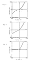
- Figs. 3, 4 and 5 show diode characteristics of the diodes fabricated from the diamond films obtained in Comparative Examples 1 and 2 and Example 1, respectively.
- The raw material to be used according to the present invention comprises a hydrogen gas, a carbon-containing compound, an oxygen-containing compound and optionally a dopant and is supplied to a reaction chamber in a vapor phase. The raw material is preferably diluted with an inert gas.
- Specific examples of the carbon-containing compound are paraffinic hydrocarbons (e.g. methane, ethane, propane, butane, etc.), olefinic hydrocarbons (e.g. ethylene, propylene, butylene, etc.), acetylene type hydrocarbons (e.g. acetylene, allylene, etc.), dienes (e.g. butadiene, etc.), alicyclic hydrocarbons (e.g. cyclopropane, cyclobutane, cyclopentane, cyclohexane, etc.), aromatic hydrocarbons (e.g. cyclobutadiene, benzene, toluene, xylene, naphthalene, etc.), ketones (e.g. acetone, diethyl ketone, benzophenone, etc.), alcohols (e.g. methanol, ethanol, etc.), amines (e.g. trimethylamine, triethylamine, etc.), carbon monoxide, carbon dioxide, and mixtures thereof. Further, the carbon-containing compound may be a compound consisting of carbon atoms such as graphite, coal and coke.
- As the oxygen-containing compound, oxygen, water, carbon monoxide, carbon dioxide and hydrogen peroxide are preferable since they are easily available.
- When carbon monoxide or carbon dioxide is used, other carbon-containing compound is not necessarily used.
- The inert gas includes argon, helium, neon, krypton, xenon and radon.
- As the dopant, elemental boron, lithium, nitrogen, phosphorus, sulfur, chlorine, arsenic or selenium and their compounds can be used.
- In the raw material, the moles of the hydrogen gas (A), the inert gas (B), the carbon atoms contained in the carbon-containing compound (C) and the oxygen atoms contained in the oxygen-containing compound (D) preferably satisfy the following equations:
0.02 ≦ C/(A+B+C+D) < 0.5 and
0.01 ≦ D/C ≦ 1. When the ratio: C/(A+B+C+D) is less than 0.02, the surface of the diamond film tends to lose its smoothness. When this ratio is 0.5 or larger, the graphite component tends to deposit. - When the ratio: D/C is less than 0.01, the crystallinity of the diamond film tends to decrease. When this ratio is larger than 1 (one), the formation of the diamond film may be inhibited.
- As the substrate, not only the single crystal diamond but also a substrate a lattice constant (a) of which satisfies the following relation can be used:
|(a - a₀)/a| x 100 ≦ 20
in which a₀ is the lattice constant of the single crystal diamond (= 3.567 Å) and a is a lattice constant of the substrate. Examples of such substrate material are magnesium oxide (a: 4.213 Å), Ni (a: 3.524 Å), Cu (a: 3.6147 Å), Ni/Cu alloy, β-SiC (a: 4.36 Å), α-SiC (a: 3.0807 Å), C-BN (a: 3.615 Å), AlN (a: 3.104 Å), PbTiO₃ (a: 3.90 Å), Ba₂TiO₄ (a: 3.994 Å), GaN (a: 3.180 Å), ZnO (a: 3.2407 Å), ZnS (a: 3.820 Å), ZrO₂ (a: 3.64 Å), oxide superconductive materials such as Tl₂Ba₂Ca₂Cu₃O₁₀ (a: 3.85 Å) or Y₁Ba₂CU₃O7-x (a: 3.89 Å) and the like. - The vapor deposition of diamond can be carried out by a conventional method such as microwave plasma CVD (chemical vapor deposition), thermal filament CVD, RF plasma CVD, DC plasma CVD, plasma jet, chemical transportation, and the like. Among them, the plasma CVD using alternating current of 1KHz or larger, particularly microwave plasma CVD is preferred, since the deposited diamond is less contaminated with impurities from a reaction chamber.
- The pressure in the reaction chamber is usually from 10⁻⁴ to 10³ Torr.
- The temperature of the substrate depends on the kind of substrate. Preferably, it is from 700 to 1000°C.
- To synthesize the single crystal diamond film having a smooth surface and good electrical characteristics, the diamond is epitaxially grown in a state in which a degree of supersaturation of the carbon-containing compound in the vapor phase is large and which is close to the thermodynamic equilibrium. When the supply amount of the carbon-containing compound is increased to increase the degree of supersaturation, the graphite component contaminates the deposited diamond film or deposits in the reaction chamber to change the process conditions, although the film smoothness of the deposited diamond is improved. When the oxygen-containing compound is added to the carbon-containing compound, the former is decomposed to generate oxygen radicals or hydroxyl radicals. These radicals accelerate the decomposition of the carbon-containing compound and react selectively with the by-produced graphite to remove it. Then, the addition of the oxygen-containing compound makes it possible to synthesize the single crystal diamond film in the supersaturated state of the carbon-containing compound in the vapor phase, whereby the single crystal diamond having the smooth surface and good electrical and optical characteristics can be produced.
- The method of the present invention will be illustrated by making reference to the accompanying drawings.
- Fig. 1 schematically shows a preferred embodiment of an apparatus for carrying out the method of the present invention. Hydrogen gas 1,
methane gas 2 as the carbon-containing compound anddiborane gas 3 are metered with respectivemass flowmeters 5, mixed and then supplied in areaction chamber 6.Oxygen gas 5 as the oxygen-containing compound is metered with amass flowmeter 5 and then supplied in thereaction chamber 6 through a supply line different from one for supplying the above mixture since the oxygen gas reacts with diborane. The gas mixture is decomposed in thechamber 6 withmicrowave 7. Carbon atoms generated through decomposition of methane is heated to several hundred degree (°C) and reaches a single crystal diamond substrate 8 to form a diamond layer and a graphite layer. The graphite layer is removed through reaction of carbon with hydrogen atoms generated by the decomposition of hydrogen or oxygen atoms generated by the decomposition of oxygen. Thereaction chamber 6 is evacuated with avacuum pump 9. - Fig. 2 is a cross section of a device for supplying a liquid material such as water and methanol to the reaction chamber in a vapor state. The
hydrogen gas 11 is metered with themass flow meter 12 and flowed through aliquid material 14 contained in aglass vessel 13. Theliquid material 14 is entrained with the hydrogen gas flow and supplied in the reaction chamber. To increase the supply amount of the liquid material, thevessel 13 can be heated with aheater 15. - The present invention will be explained further in detail by following examples.
- A single crystal diamond film was grown by using the apparatus of Fig. 1. The reaction chamber was made of quartz and had an inner diameter of 44 mm and a length of 600 mm. As a substrate, a diamond single crystal of 1.5 mm in length, 2.0 mm in width and 0.3 mm in thickness was used with the (100) plane forming a deposition surface. As the raw material, a mixture of methane, hydrogen, diborane and oxygen in a molar ratio of Table 1 (Example 1) or a mixture of methane, hydrogen and diborane in a molar ratio of Table 1 (Comparative Examples 1 and 2) was used. The total flow rate of the raw material was 100 sccm. The microwave having a frequency of 2.45 Hz and power of 300 W was used. The deposited diamond film had a thickness of about 1 µm. Other reaction conditions are shown in Table 1.
Table 1 Example No. 1 Comp. 1 Comp. 2 Raw material (mole %) H₂ 89 % H₂ 99 % H₂ 90 % CH₄ 10 % CH₄ 1 % CH₄ 10 % B₂H₆ 20 ppm B₂H₆ 20 ppm B₂H₆ 20 ppm O₂ 1 % Pressure (Torr) 40 40 40 Substrate temp. (°C) 830 830 830 Reaction time (hrs) 2 2 2 - In Comparative Example 1, although the good quality diamond film containing no graphite component was produced, the surface roughness was about 2000 Å. When the amount of methane was increased as in Comparative Example 2, although the diamond film having surface roughness of less than 100 Å was produced, the presence of the amorphous component was confirmed by electron diffraction analysis.
- In Example 1, the diamond film had surface roughness of less than 100 Å and the electron diffraction gave a streak pattern which indicates a single crystal having uniformity in the atomic level.
- Electrodes were formed on the obtained diamond film to assemble a Schottky diode. The characteristics of the diode were evaluated from a forward direction current If and a reverse direction leak current Ir in the diode.
- With the diode which was fabricated from the diamond film obtained in Comparative Example 1 or 2, an amount of Ir is more than one tenth of If, and no good rectification was achieved. The diode characteristics in Comparative Examples 1 and 2 are shown in Figs. 3 and 4, respectively.
- With the diode which was fabricated from the diamond film obtained in Example 1, an amount of Ir was less than one thousandth of If, and good rectification was achieved. The diode characteristics in Example 1 is shown in Fig. 5.
- The properties of the deposited diamond films in Example 1 and Comparative Examples 1 and 2 are summarized in Table 2.
Table 2 Example No. 1 Comp. 1 Comp. 2 Surface roughness (Å) <100 ca. 2000 <100 Crystallinity Complete single crystal Partly crystallized Partly amorphous Electron diffraction pattern Streak patter Streak pattern + ring patter Halo pattern Diode characteristics Ir<If/1000 see Fig. 5 Ir<If/10 see Fig. 3 Ir<If/10 see Fig. 4 -
- In the same manner as in Example 1 but supplying hydrogen gas at 100 sccm, methane at 10 sccm, diborane (diluted with hydrogen to 10 ppm) at 10 sccm and carbon dioxide at 2 sccm in the reaction chamber and reacting them at a substrate temperature of 830°C under pressure of 40 Torr for 2 hours to deposit a diamond film of 1.2 µm in thickness. The diamond film was a single crystal with good crystallinity and surface roughness of less than 100 Å, and had high hole mobility of about 1000 cm²/V.sec. A Schottky diode fabricated from this diamond film achieved good rectification.
- In the same manner as above but using no carbon dioxide, a diamond film was deposited on the substrate. The diamond film contained a graphite component and had neither good crystallinity nor electrical characteristics.
- In the same manner as in Example 1 but supplying hydrogen gas at 100 sccm, methane at 10 sccm, diborane (diluted with hydrogen to 10 ppm) at 10 sccm and carbon monoxide at 3 sccm in the reaction chamber and reacting them at a substrate temperature of 830°C under pressure of 40 Torr for 2 hours to deposit a diamond film of 1.5 µm in thickness. The diamond film was a single crystal with good crystallinity and surface roughness of less than 100 Å, and had high hole mobility of about 1000 cm²/V.sec. A Schottky diode fabricated from this diamond film achieved good rectification.
- In the same manner as above but using no carbon monoxide, a diamond film was deposited on the substrate. The diamond film contained a graphite component and had neither good crystallinity nor electrical characteristics.
- In the same manner as in Example 1 but supplying hydrogen gas at 100 sccm, argon at 50 sccm, methane at 15 sccm, diborane (diluted with hydrogen to 10 ppm) at 10 sccm and oxygen at 2 sccm in the reaction chamber and reacting them at a substrate temperature of 850°C under pressure of 80 Torr for 2 hours to deposit a diamond film of 2 µm in thickness. The diamond film was a single crystal with good crystallinity and surface roughness of less than 100 Å, and had high hole mobility of about 1000 cm²/V.sec. A Schottky diode fabricated from this diamond film achieved good rectification.
- In the same manner as above but using no oxygen, a diamond film was deposited on the substrate. The diamond film contained a graphite component and had neither good crystallinity nor electrical characteristics.
- Since the supply of the inert gas in the reaction chamber stabilizes the supersaturation of the carbon-containing compound in the vapor phase, the diamond with good quality can be epitaxially grown at a growth rate at least twice larger than in case of the absence of the inert gas.
- In the same manner as in Example 1 but supplying hydrogen gas at 100 sccm in total, methane at 10 sccm, diborane (diluted with hydrogen to 10 ppm) at 10 sccm and water at 2 sccm (as converted to a saturated vapor pressure) in the reaction chamber and reacting them at a substrate temperature of 830°C under pressure of 40 Torr for 2 hours to deposit a diamond film of 1.1 µm in thickness. To supply water, the device of Fig. 2 was used. The diamond film was a single crystal with good crystallinity and surface roughness of less than 100 Å, and had high hole mobility of about 1000 cm²/V.sec. A Schottky diode fabricated from this diamond film achieved good rectification.
- In the same manner as above but using no water, a diamond film was deposited on the substrate. The diamond film contained a graphite component and had neither good crystallinity nor electrical characteristics.
-
- In the same manner as in Example 1 but supplying hydrogen gas at 100 sccm in total, methanol at 8 sccm (as converted to a saturated vapor pressure), diborane (diluted with hydrogen to 10 ppm) at 10 sccm and oxygen at 1 sccm in the reaction chamber and reacting them at a substrate temperature of 830°C under pressure of 40 Torr for 2 hours to deposit a diamond film of 1.5 µm in thickness. The diamond film was a single crystal with good crystallinity and surface roughness of less than 100 Å, and had high hole mobility of about 1000 cm²/V.sec. A Schottky diode fabricated from this diamond film achieved good rectification.
- In the same manner as above but using no oxygen, a diamond film was deposited on the substrate. The diamond film contained a graphite component and had neither good crystallinity nor electrical characteristics.
- When the alcohol is used as the carbon source, the high quality diamond film can be epitaxially grown at low cost.
- In the same manner as in Example 1 but using a MgO substrate with the (100) plane forming the deposition surface, supplying hydrogen gas at 50 sccm, argon at 50 sccm, methane at 10 sccm, diborane (diluted with hydrogen to 10 ppm) at 10 sccm and oxygen at 2 sccm in the reaction chamber and reacting them at a substrate temperature of 800°C under pressure of 40 Torr for 2 hours to deposit a diamond film of 0.9 µm in thickness. The diamond film was a single crystal with good crystallinity and surface roughness of less than 100 Å. A Schottky diode fabricated from this diamond film achieved good rectification.
- In the same manner as above but using no oxygen, a diamond film was deposited on the substrate. The MgO substrate was partly reduced, and the diamond film contained a graphite component and had no good crystallinity.
- According to the present invention, the single crystal diamond film with good crystallinity and a smooth surface can be epitaxially grown on the single crystal substrate, and the high quality single diamond, which has been obtained from a natural source or by the ultra-high pressure method, can be easily synthesized by the vapor deposition method. The electric device fabricated from the diamond film produced according to the present invention has good electrical characteristics and is ambient resistance.
- When the diamond film has a large thickness, it can be used as an optical element or a heat sink. Since a large size diamond particle can be produced with keeping good crystallinity, abrasive particles or a jewel can be prepared.
Claims (10)
0.02 ≦ C/(A+B+C+D) < 0.5 and
0.01 ≦ D/C ≦ 1.
|(a - a₀)/a| x 100 ≦ 20
wherein a₀ is the lattice constant of the single crystal diamond and a is a lattice constant of the substrate compound.
Applications Claiming Priority (2)
| Application Number | Priority Date | Filing Date | Title |
|---|---|---|---|
| JP54476/89 | 1989-03-07 | ||
| JP1054476A JP2730144B2 (en) | 1989-03-07 | 1989-03-07 | Single crystal diamond layer formation method |
Publications (2)
| Publication Number | Publication Date |
|---|---|
| EP0386727A1 true EP0386727A1 (en) | 1990-09-12 |
| EP0386727B1 EP0386727B1 (en) | 1994-06-15 |
Family
ID=12971723
Family Applications (1)
| Application Number | Title | Priority Date | Filing Date |
|---|---|---|---|
| EP90104346A Expired - Lifetime EP0386727B1 (en) | 1989-03-07 | 1990-03-07 | Method for producing single crystal diamond film |
Country Status (4)
| Country | Link |
|---|---|
| US (1) | US5400738A (en) |
| EP (1) | EP0386727B1 (en) |
| JP (1) | JP2730144B2 (en) |
| DE (1) | DE69009799T2 (en) |
Cited By (6)
| Publication number | Priority date | Publication date | Assignee | Title |
|---|---|---|---|---|
| DE4027580A1 (en) * | 1990-08-31 | 1992-03-05 | Lux Benno | COMPOSITE BODY, METHOD FOR THE PRODUCTION AND USE THEREOF |
| EP0611331A4 (en) * | 1991-11-05 | 1995-01-11 | Res Triangle Inst | VAPOR DEPOSITION BY CHEMICAL PROCESS OF THIN FILMS OF DIAMOND USING WATER-BASED PLASMA DISCHARGES. |
| US5704976A (en) * | 1990-07-06 | 1998-01-06 | The United States Of America As Represented By The Secretary Of The Navy | High temperature, high rate, epitaxial synthesis of diamond in a laminar plasma |
| WO2003052174A3 (en) * | 2001-12-14 | 2003-10-02 | Element Six Ltd | Boron doped diamond |
| GB2433737A (en) * | 2002-11-21 | 2007-07-04 | Element Six Ltd | A CVD single crystal diamond material |
| US8936774B2 (en) | 2002-11-21 | 2015-01-20 | Element Six Technologies Limited | Optical quality diamond material |
Families Citing this family (12)
| Publication number | Priority date | Publication date | Assignee | Title |
|---|---|---|---|---|
| JP3491237B2 (en) * | 1993-09-24 | 2004-01-26 | 日本テキサス・インスツルメンツ株式会社 | Stacked conductive film structure of semiconductor device |
| JP3051912B2 (en) * | 1996-09-03 | 2000-06-12 | 科学技術庁無機材質研究所長 | Synthesis method of phosphorus-doped diamond |
| GB2379451B (en) * | 2000-06-15 | 2004-05-05 | Element Six | Thick single crystal diamond layer method for making it and gemstones produced from the layer |
| US6833027B2 (en) * | 2001-09-26 | 2004-12-21 | The United States Of America As Represented By The Secretary Of The Navy | Method of manufacturing high voltage schottky diamond diodes with low boron doping |
| GB0130004D0 (en) * | 2001-12-14 | 2002-02-06 | Diamanx Products Ltd | Coloured diamond |
| JP4759315B2 (en) * | 2004-05-21 | 2011-08-31 | 独立行政法人物質・材料研究機構 | Boron-doped diamond thin film with superconductivity |
| EP2431503A1 (en) * | 2004-05-27 | 2012-03-21 | Toppan Printing Co., Ltd. | Method of manufacturing an organic electroluminescent device or an organic photoelectric receiving device using a nano-crystalline diamond film |
| JP2009525944A (en) * | 2006-02-07 | 2009-07-16 | ターゲット・テクノロジー・カンパニー・エルエルシー | Materials and methods for producing large diamond crystals |
| GB0813490D0 (en) * | 2008-07-23 | 2008-08-27 | Element Six Ltd | Solid state material |
| GB0813491D0 (en) | 2008-07-23 | 2008-08-27 | Element Six Ltd | Diamond Material |
| US10273598B2 (en) * | 2009-12-22 | 2019-04-30 | Element Six Technologies Limited | Synthetic CVD diamond |
| WO2025250682A1 (en) * | 2024-05-28 | 2025-12-04 | Serenity Technologies | Gem quality diamond synthesis from alternative carbon sources |
Citations (1)
| Publication number | Priority date | Publication date | Assignee | Title |
|---|---|---|---|---|
| EP0282054A1 (en) * | 1987-03-12 | 1988-09-14 | Sumitomo Electric Industries Limited | Thin film single crystal diamond substrate |
Family Cites Families (15)
| Publication number | Priority date | Publication date | Assignee | Title |
|---|---|---|---|---|
| US3630678A (en) * | 1968-06-26 | 1971-12-28 | Univ Case Western Reserve | Diamond growth process |
| US3961103A (en) * | 1972-07-12 | 1976-06-01 | Space Sciences, Inc. | Film deposition |
| JPS59154965A (en) * | 1983-02-22 | 1984-09-04 | Tamagawa Kikai Kk | Fish processor |
| JPS59164607A (en) * | 1983-03-11 | 1984-09-17 | Showa Denko Kk | Method for synthesizing diamond |
| JPS60127298A (en) * | 1983-12-09 | 1985-07-06 | Sumitomo Electric Ind Ltd | Diamond vapor phase synthesis method |
| JPS60191097A (en) * | 1984-03-08 | 1985-09-28 | Mitsubishi Metal Corp | Crystallizing method of artificial diamond |
| JPS61183198A (en) * | 1984-12-29 | 1986-08-15 | Kyocera Corp | Production of diamond film |
| JPS61158899A (en) * | 1985-07-31 | 1986-07-18 | Kyocera Corp | Production of diamond film |
| JPS6270295A (en) * | 1985-09-24 | 1987-03-31 | Sumitomo Electric Ind Ltd | Manufacturing method of n-type semiconductor diamond film |
| JPS632897A (en) * | 1986-06-21 | 1988-01-07 | Yoichi Hirose | Method for synthesizing diamond by vapor phase method |
| JPH0768078B2 (en) * | 1986-07-11 | 1995-07-26 | 京セラ株式会社 | Diamond film manufacturing method |
| US5373171A (en) * | 1987-03-12 | 1994-12-13 | Sumitomo Electric Industries, Ltd. | Thin film single crystal substrate |
| JPS63252997A (en) * | 1987-04-07 | 1988-10-20 | Sharp Corp | Production of diamond single crystal |
| JPH01197391A (en) * | 1988-02-01 | 1989-08-09 | Idemitsu Petrochem Co Ltd | Method for synthesizing diamond |
| JPH01290592A (en) * | 1988-05-16 | 1989-11-22 | Idemitsu Petrochem Co Ltd | Method for synthesizing diamond |
-
1989
- 1989-03-07 JP JP1054476A patent/JP2730144B2/en not_active Expired - Fee Related
-
1990
- 1990-03-07 DE DE69009799T patent/DE69009799T2/en not_active Expired - Fee Related
- 1990-03-07 EP EP90104346A patent/EP0386727B1/en not_active Expired - Lifetime
-
1992
- 1992-12-08 US US07/987,557 patent/US5400738A/en not_active Expired - Lifetime
Patent Citations (1)
| Publication number | Priority date | Publication date | Assignee | Title |
|---|---|---|---|---|
| EP0282054A1 (en) * | 1987-03-12 | 1988-09-14 | Sumitomo Electric Industries Limited | Thin film single crystal diamond substrate |
Non-Patent Citations (10)
| Title |
|---|
| JAPANESE JOURNAL OF APPLIED PHYSICS/PART 1: REGULAR PAPERS & SHORT NOTES, vol. 26, no. 9, September 1987, pages 1429-1432, Tokyo, JP; T. KAWATO et al.: "Effects of oxygen on CVD diamond synthesis" * |
| JOURNAL OF APPLIED PHYSICS, vol. 63, no. 5, 1st March 1988, pages 1744-1748, American Institute of Physics, Woodbury, NY, US; C.-P. CHANG et al.: "Diamond crystal growth by plasma chemical vapor deposition" * |
| PATENT ABSTRACTS OF JAPAN, vol. 10, no. 362 (C-389)[2419], 4th December 1986; & JP-A-61 158 899 (KYOCERA CORP.) 18-07-1986 * |
| PATENT ABSTRACTS OF JAPAN, vol. 10, no. 43 (C-329)[2100], 20th February 1986; & JP-A-60 191 097 (MITSUBISHI KINZOKU K.K.) 28-09-1985 * |
| PATENT ABSTRACTS OF JAPAN, vol. 11, no. 267 (C-443)[2714], 28th August 1987; & JP-A-62 070 295 (SUMITOMO ELECTRIC IND. LTD) 31-03-1987 * |
| PATENT ABSTRACTS OF JAPAN, vol. 11, no. 3 (C-395)[2450], 7th January 1987; & JP-A-61 183 198 (KYOCERA CORP.) 15-08-1986 * |
| PATENT ABSTRACTS OF JAPAN, vol. 12, no. 198 (C-502)[3045], 8th June 1988; & JP-A-63 002 897 (YOICHI HIROSE) 07-01-1988 * |
| PATENT ABSTRACTS OF JAPAN, vol. 12, no. 223 (C-507)[3070], 24th June 1988; & JP-A-63 021 291 (KYOCERA CORP.) 28-01-1988 * |
| PATENT ABSTRACTS OF JAPAN, vol. 13, no. 61 (C-567)[3409], 10th February 1989; & JP-A-63 252 997 (SHARP CORP.) 20-10-1988 * |
| VACUUM, vol. 36, nos. 1-3, 1986, pages 99-102, Pergamon Press Ltd, London, GB; N. FUJIMORI et al.: "Characterization of conducting diamond films" * |
Cited By (15)
| Publication number | Priority date | Publication date | Assignee | Title |
|---|---|---|---|---|
| US5704976A (en) * | 1990-07-06 | 1998-01-06 | The United States Of America As Represented By The Secretary Of The Navy | High temperature, high rate, epitaxial synthesis of diamond in a laminar plasma |
| DE4027580A1 (en) * | 1990-08-31 | 1992-03-05 | Lux Benno | COMPOSITE BODY, METHOD FOR THE PRODUCTION AND USE THEREOF |
| US5296207A (en) * | 1990-08-31 | 1994-03-22 | Benno Lux | Composite element, process for its preparation and its use |
| EP0611331A4 (en) * | 1991-11-05 | 1995-01-11 | Res Triangle Inst | VAPOR DEPOSITION BY CHEMICAL PROCESS OF THIN FILMS OF DIAMOND USING WATER-BASED PLASMA DISCHARGES. |
| GB2400116B (en) * | 2001-12-14 | 2005-06-22 | Element Six Ltd | Boron doped diamond |
| GB2400116A (en) * | 2001-12-14 | 2004-10-06 | Element Six Ltd | Boron doped diamond |
| WO2003052174A3 (en) * | 2001-12-14 | 2003-10-02 | Element Six Ltd | Boron doped diamond |
| CN1321227C (en) * | 2001-12-14 | 2007-06-13 | 六号元素有限公司 | Boron doped diamond |
| EP1780315A3 (en) * | 2001-12-14 | 2010-02-24 | Element Six Limited | Boron doped diamond |
| GB2433737A (en) * | 2002-11-21 | 2007-07-04 | Element Six Ltd | A CVD single crystal diamond material |
| GB2433737B (en) * | 2002-11-21 | 2007-08-15 | Element Six Ltd | Optical quality diamond material |
| US8936774B2 (en) | 2002-11-21 | 2015-01-20 | Element Six Technologies Limited | Optical quality diamond material |
| US9551090B2 (en) | 2002-11-21 | 2017-01-24 | Element Six Technologies Limited | Optical quality diamond material |
| US10125434B2 (en) | 2002-11-21 | 2018-11-13 | Element Six Technologies Limited | Optical quality diamond material |
| US10851471B2 (en) | 2002-11-21 | 2020-12-01 | Element Six Technologies Limited | Optical quality diamond material |
Also Published As
| Publication number | Publication date |
|---|---|
| US5400738A (en) | 1995-03-28 |
| JPH02233590A (en) | 1990-09-17 |
| JP2730144B2 (en) | 1998-03-25 |
| DE69009799T2 (en) | 1994-11-17 |
| EP0386727B1 (en) | 1994-06-15 |
| DE69009799D1 (en) | 1994-07-21 |
Similar Documents
| Publication | Publication Date | Title |
|---|---|---|
| US5387310A (en) | Method for producing single crystal diamond film | |
| US5400738A (en) | Method for producing single crystal diamond film | |
| Koizumi et al. | Epitaxial growth of diamond thin films on cubic boron nitride {111} surfaces by dc plasma chemical vapor deposition | |
| US4923716A (en) | Chemical vapor desposition of silicon carbide | |
| EP0632145B1 (en) | Method of forming crystalline silicon carbide coatings | |
| EP0282075B1 (en) | Thin film single crystal substrate | |
| EP0442304B1 (en) | Polycrystalline CVD diamond substrate for single crystal epitaxial growth of semiconductors | |
| US4623425A (en) | Method of fabricating single-crystal substrates of silicon carbide | |
| EP0322615B1 (en) | Method of growing a single crystalline beta-silicon carbide layer on a silicon substrate | |
| Takahashi et al. | Low‐temperature growth of 3 C‐SiC on Si substrate by chemical vapor deposition using hexamethyldisilane as a source material | |
| EP0030638A1 (en) | Method for depositing silicon or germanium containing films | |
| US4897149A (en) | Method of fabricating single-crystal substrates of silicon carbide | |
| US20120103250A1 (en) | Film of n type (100) oriented single crystal diamond semiconductor doped with phosphorous atoms, and a method of producing the same | |
| AU614605B2 (en) | Diamond growth | |
| US6911084B2 (en) | Low temperature epitaxial growth of quaternary wide bandgap semiconductors | |
| US5863324A (en) | Process for producing single crystal diamond film | |
| US5043219A (en) | Composite material | |
| JP3467988B2 (en) | Semiconductor manufacturing method and semiconductor manufacturing apparatus | |
| Itoh et al. | Observations of growth process of chemically vapor deposited diamond single crystal | |
| Yamashita et al. | Homoepitaxial chemical vapor deposition of 6H-SiC at low temperatures on {0114} substrates | |
| JPH0754802B2 (en) | Vapor growth method of GaAs thin film | |
| JPS6115150B2 (en) | ||
| JP3932017B2 (en) | Method for producing iron silicide crystal | |
| JPS63129609A (en) | Method of adding impurity for iii-v compound semiconductor single crystal thin film | |
| JPS62224674A (en) | Manufacture of microcrystalline silicon carbide film |
Legal Events
| Date | Code | Title | Description |
|---|---|---|---|
| PUAI | Public reference made under article 153(3) epc to a published international application that has entered the european phase |
Free format text: ORIGINAL CODE: 0009012 |
|
| AK | Designated contracting states |
Kind code of ref document: A1 Designated state(s): DE FR GB |
|
| 17P | Request for examination filed |
Effective date: 19901220 |
|
| 17Q | First examination report despatched |
Effective date: 19930222 |
|
| GRAA | (expected) grant |
Free format text: ORIGINAL CODE: 0009210 |
|
| AK | Designated contracting states |
Kind code of ref document: B1 Designated state(s): DE FR GB |
|
| REF | Corresponds to: |
Ref document number: 69009799 Country of ref document: DE Date of ref document: 19940721 |
|
| ET | Fr: translation filed | ||
| PLBE | No opposition filed within time limit |
Free format text: ORIGINAL CODE: 0009261 |
|
| STAA | Information on the status of an ep patent application or granted ep patent |
Free format text: STATUS: NO OPPOSITION FILED WITHIN TIME LIMIT |
|
| 26N | No opposition filed | ||
| REG | Reference to a national code |
Ref country code: GB Ref legal event code: IF02 |
|
| PGFP | Annual fee paid to national office [announced via postgrant information from national office to epo] |
Ref country code: DE Payment date: 20050304 Year of fee payment: 16 |
|
| PGFP | Annual fee paid to national office [announced via postgrant information from national office to epo] |
Ref country code: FR Payment date: 20050308 Year of fee payment: 16 |
|
| PG25 | Lapsed in a contracting state [announced via postgrant information from national office to epo] |
Ref country code: DE Free format text: LAPSE BECAUSE OF NON-PAYMENT OF DUE FEES Effective date: 20061003 |
|
| REG | Reference to a national code |
Ref country code: FR Ref legal event code: ST Effective date: 20061130 |
|
| PG25 | Lapsed in a contracting state [announced via postgrant information from national office to epo] |
Ref country code: FR Free format text: LAPSE BECAUSE OF NON-PAYMENT OF DUE FEES Effective date: 20060331 |
|
| PGFP | Annual fee paid to national office [announced via postgrant information from national office to epo] |
Ref country code: GB Payment date: 20090304 Year of fee payment: 20 |
|
| REG | Reference to a national code |
Ref country code: GB Ref legal event code: PE20 Expiry date: 20100306 |
|
| PG25 | Lapsed in a contracting state [announced via postgrant information from national office to epo] |
Ref country code: GB Free format text: LAPSE BECAUSE OF EXPIRATION OF PROTECTION Effective date: 20100306 |