EP0383743B1 - Thin film transistor - Google Patents
Thin film transistor Download PDFInfo
- Publication number
- EP0383743B1 EP0383743B1 EP90850065A EP90850065A EP0383743B1 EP 0383743 B1 EP0383743 B1 EP 0383743B1 EP 90850065 A EP90850065 A EP 90850065A EP 90850065 A EP90850065 A EP 90850065A EP 0383743 B1 EP0383743 B1 EP 0383743B1
- Authority
- EP
- European Patent Office
- Prior art keywords
- semiconductor layer
- layer
- drain
- source
- thin film
- Prior art date
- Legal status (The legal status is an assumption and is not a legal conclusion. Google has not performed a legal analysis and makes no representation as to the accuracy of the status listed.)
- Expired - Lifetime
Links
- 239000010409 thin film Substances 0.000 title claims description 17
- 239000004065 semiconductor Substances 0.000 claims description 32
- 229910021417 amorphous silicon Inorganic materials 0.000 claims description 14
- 230000032683 aging Effects 0.000 description 4
- 239000011651 chromium Substances 0.000 description 3
- VYZAMTAEIAYCRO-UHFFFAOYSA-N Chromium Chemical compound [Cr] VYZAMTAEIAYCRO-UHFFFAOYSA-N 0.000 description 2
- 229910052581 Si3N4 Inorganic materials 0.000 description 2
- XAGFODPZIPBFFR-UHFFFAOYSA-N aluminium Chemical compound [Al] XAGFODPZIPBFFR-UHFFFAOYSA-N 0.000 description 2
- 229910052782 aluminium Inorganic materials 0.000 description 2
- 239000000969 carrier Substances 0.000 description 2
- 238000005530 etching Methods 0.000 description 2
- 230000005669 field effect Effects 0.000 description 2
- 239000010408 film Substances 0.000 description 2
- 239000000463 material Substances 0.000 description 2
- HQVNEWCFYHHQES-UHFFFAOYSA-N silicon nitride Chemical compound N12[Si]34N5[Si]62N3[Si]51N64 HQVNEWCFYHHQES-UHFFFAOYSA-N 0.000 description 2
- 239000000758 substrate Substances 0.000 description 2
- ZOKXTWBITQBERF-UHFFFAOYSA-N Molybdenum Chemical compound [Mo] ZOKXTWBITQBERF-UHFFFAOYSA-N 0.000 description 1
- 230000002411 adverse Effects 0.000 description 1
- 238000013459 approach Methods 0.000 description 1
- 229910052804 chromium Inorganic materials 0.000 description 1
- 239000002131 composite material Substances 0.000 description 1
- 230000003247 decreasing effect Effects 0.000 description 1
- 238000010586 diagram Methods 0.000 description 1
- 230000001747 exhibiting effect Effects 0.000 description 1
- 230000006355 external stress Effects 0.000 description 1
- 239000011521 glass Substances 0.000 description 1
- 238000002513 implantation Methods 0.000 description 1
- 239000012212 insulator Substances 0.000 description 1
- 238000004519 manufacturing process Methods 0.000 description 1
- 238000000034 method Methods 0.000 description 1
- 229910052750 molybdenum Inorganic materials 0.000 description 1
- 239000011733 molybdenum Substances 0.000 description 1
- 238000005268 plasma chemical vapour deposition Methods 0.000 description 1
- HBMJWWWQQXIZIP-UHFFFAOYSA-N silicon carbide Chemical compound [Si+]#[C-] HBMJWWWQQXIZIP-UHFFFAOYSA-N 0.000 description 1
- 229910010271 silicon carbide Inorganic materials 0.000 description 1
- 238000004544 sputter deposition Methods 0.000 description 1
Images

Classifications
-
- H—ELECTRICITY
- H10—SEMICONDUCTOR DEVICES; ELECTRIC SOLID-STATE DEVICES NOT OTHERWISE PROVIDED FOR
- H10D—INORGANIC ELECTRIC SEMICONDUCTOR DEVICES
- H10D30/00—Field-effect transistors [FET]
- H10D30/60—Insulated-gate field-effect transistors [IGFET]
- H10D30/67—Thin-film transistors [TFT]
- H10D30/674—Thin-film transistors [TFT] characterised by the active materials
- H10D30/6741—Group IV materials, e.g. germanium or silicon carbide
- H10D30/6748—Group IV materials, e.g. germanium or silicon carbide having a multilayer structure or superlattice structure
-
- H—ELECTRICITY
- H10—SEMICONDUCTOR DEVICES; ELECTRIC SOLID-STATE DEVICES NOT OTHERWISE PROVIDED FOR
- H10D—INORGANIC ELECTRIC SEMICONDUCTOR DEVICES
- H10D30/00—Field-effect transistors [FET]
- H10D30/60—Insulated-gate field-effect transistors [IGFET]
- H10D30/67—Thin-film transistors [TFT]
- H10D30/6729—Thin-film transistors [TFT] characterised by the electrodes
- H10D30/673—Thin-film transistors [TFT] characterised by the electrodes characterised by the shapes, relative sizes or dispositions of the gate electrodes
- H10D30/6732—Bottom-gate only TFTs
-
- H—ELECTRICITY
- H10—SEMICONDUCTOR DEVICES; ELECTRIC SOLID-STATE DEVICES NOT OTHERWISE PROVIDED FOR
- H10D—INORGANIC ELECTRIC SEMICONDUCTOR DEVICES
- H10D30/00—Field-effect transistors [FET]
- H10D30/60—Insulated-gate field-effect transistors [IGFET]
- H10D30/67—Thin-film transistors [TFT]
- H10D30/674—Thin-film transistors [TFT] characterised by the active materials
- H10D30/6741—Group IV materials, e.g. germanium or silicon carbide
- H10D30/6743—Silicon
- H10D30/6746—Amorphous silicon
Definitions
- This invention relates to a thin film transistor.
- FIG.2 An example of a conventional amorphous silicon thin film transistor is shown in Fig.2.
- a transparent insulating substrate 21 is provided thereon with a gate electrode 22 using chrome (Cr), and a gate insulating layer 23 that consists of silicon nitride formed by a plasma CVD process.
- a semiconductor layer 24 using amorphous silicon is formed on the gate insulating layer 23, and a source electrode 25 and a drain electrode 26 are formed by aluminum (A1).
- Figure 3 shows the electrical characteristics of the conventional amorphous silicon thin film transistor shown in Figure 5.
- the curve (1) of Figure 6 shows the drain current-gate voltage (Id-Vg) characteristics at an initial state where the voltage between the source and the drain (Vsd) was set for 10 volts.
- the threshold voltage (Vth) at the moment was 1.2 volts.
- the curve (3) of Figure 3 similarly shows the Id-Vg characteristics after applying -10 volts to the gate voltage and leaving for 96 hours.
- the threshold voltage of the curves (2) and (3) of Figure 6 is 2.1 and -0.3 volts, respectively.
- the threshold voltage (Vth) shifts in the positive direction when a positive potential is applied to the gate voltage and left, and in the negative direction when negative potential is applied and left.
- the amount of the shift is particularly significant in the positive direction.
- the variation of the threshold voltage (Vth) appears to be caused by the fact that electric charges are implanted in the gate insulating layer 23.
- Vth threshold voltage
- the invention is made in view of the above problems, and its object is to provide a thin film transistor exhibiting high reliability and high performance while holding the variation of its threshold voltage at the minimum level.
- Such buffer layers between the gate insulating layer and the semiconductor layer can permit the ageing variation of the threshold voltage (Vth) to be decreased, and the variations of the threshold voltage (Vth) within each production lot to be suppressed.
- the variation of the threshold voltage (Vth) seems to be caused by the fact that the electric charge flowing into the insulating layer or captured in an interface causes a change in the amount of the effective charge induced in the surface of the semiconductor layer.
- Such variation of the threshold voltage (Vth) is particularly significant when the semiconductor layer consists of amorphous material. Suppressing of the variation is also important because the amorphous semiconductor is widely used.
- the buffer layer contributes to reduce the change of the amount of the effective charge induced in the surface of the semiconductor. That is, the buffer layer in place of the semiconductor layer interacts with the insulating layer so as to prevent the effective charge in the semiconductor layer from being reduced.
- buffer layers which function in the above manner typically have a carrier density higher than that of the semiconductor layer, so that it may become a path of source-drain current adversely affecting the performance of the device.
- a thin film transistor comprising a gate electrode, a gate insulating layer, a semiconductor layer, a buffer layer provided between the gate insulating layer and the semiconductor layer, a source electrode and a drain electrode, characterised in that the carrier density of said buffer layer is higher than that of said semiconductor layer and said buffer layer is separated into a source section and a drain section.
- a symmetrical arrangement is employed in which the gate electrode is positioned on one side of the gate insulating layer and the buffer layer of high carrier density is positioned on the other side of the gate insulating layer, while the buffer layer is positioned on one side of the semiconductor layer and the source and the drain electrodes are positioned on the other side of the semiconductor layer.
- This symmetry and the high carrier density in the buffer layer enables the ageing variation of the threshold voltage to be suppressed and a high ON current between the source and the drain to be obtained because carriers are previously dispersed in the insulating layer.
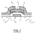
- FIGURE 1 is a cross section of a thin film transistor embodying the invention.
- FIGURE 2 is a cross section of an example of a conventional amorphous silicon thin film transistor.
- FIGURE 3 is a diagram showing the drain current-gate voltage characteristics of a thin film transistor with a conventional structure.
- Figure 1 shows a cross section of a thin film transistor embodying the invention.
- the thin film transistor according to this embodiment consists of a gate electrode 2, a gate insulating layer 3 and a semiconductor layer 5, a buffer layer 4 provided between the gate insulating layer 3 and the semiconductor layer 5, a source electrode 6 and a drain layer 7.
- the gate electrode 2 is formed by chromium (Cr) in a thickness of 300 nm (3,000 angstroms) on a transparent insulating substrate 11 consisting of glass.
- a gate insulating layer 3 is formed on the gate electrode 2 by a silicon nitride film in a thickness of 200 nm (2,000 angstroms).
- the buffer layer 4 is formed by molybdenum (Mo) with a thickness of 30 nm (300 angstroms) following surface light etching of by a sputtering device.
- Mo molybdenum
- the buffer layer 4 is formed by separating into a section below the source electrode 6 and a section below the drain electrode 7.
- the semiconductor layer 5 is formed on the buffer layer 4 by a phospor doped amorphous silicon (n+-a-Si) and an amorphous silicon film (a-Si) in a thickness of 200 nm (2,000 angstroms).
- the source electrode 6 and the drain electrode 7 are also formed on it by aluminum (A1).
- the buffer layer 4 serves to reduce change of the amount of effective charge induced on the surface of the semiconductor layer 5. That is, the buffer layer 4 in place of the semiconductor layer interacts with the insulating layer 3 so as to prevent the effective charge in the semiconductor layer from being reduced. To this end, as described above, the buffer layer 4 is formed by a material having a higher carrier density than that of the semiconductor layer 5.
- the buffer layer 4 may become a path of source-drain current, so that the buffer layer with high carrier density is separated into a section below the source electrode 6 and a section below the drain electrode 7.
- a symmetrical arrangement is employed in which the gate electrode 2 is positioned on one side of the gate insulating layer 3 and the two sections of the buffer layer 4 are framed on the other side of the gate insulating layer 3, in the semiconductor layer 5 and aligned respectively with the source electrode 6 and the drain electrode 7, which are positioned on the other side of the semiconductor layer 5.
- channel width/channel length 40 ⁇ m/10 ⁇ m.
- the invention provides a thin film transistor that can reduce the ageing variation of the threshold voltage, and can be stably driven by making the energy band gap width of the buffer provided between the gate insulating layer and the semiconductor layer wider than that of the semiconductor layer, or by making the carrier density of the buffer layer higher than that of the semiconductor layer.
- higher ON current between the source and the drain can be obtained by making the carrier density of the buffer layer higher than that of the semiconductor layer, and by separating the buffer layer into the source section and the drain section.
Landscapes
- Thin Film Transistor (AREA)
- Formation Of Insulating Films (AREA)
Description
- This invention relates to a thin film transistor.
- An example of a conventional amorphous silicon thin film transistor is shown in Fig.2. A transparent
insulating substrate 21 is provided thereon with agate electrode 22 using chrome (Cr), and a gate insulating layer 23 that consists of silicon nitride formed by a plasma CVD process. Asemiconductor layer 24 using amorphous silicon is formed on the gate insulating layer 23, and asource electrode 25 and adrain electrode 26 are formed by aluminum (A1). - Figure 3 shows the electrical characteristics of the conventional amorphous silicon thin film transistor shown in Figure 5. The curve (1) of Figure 6 shows the drain current-gate voltage (Id-Vg) characteristics at an initial state where the voltage between the source and the drain (Vsd) was set for 10 volts. The threshold voltage (Vth) at the moment was 1.2 volts. The curve (2) of Figure 6 shows the Id-Vg characteristics after applying +25 volts to the gate voltage of this amorphous silicon thin film transistor with constant source-drain voltage (Vsd) = 10 volts, leaving it for 96 hours. The curve (3) of Figure 3 similarly shows the Id-Vg characteristics after applying -10 volts to the gate voltage and leaving for 96 hours. The threshold voltage of the curves (2) and (3) of Figure 6 is 2.1 and -0.3 volts, respectively.
- As seen from Figure 3, in the conventional amorphous silicon thin film transistor with the structure of Figure 2, the threshold voltage (Vth) shifts in the positive direction when a positive potential is applied to the gate voltage and left, and in the negative direction when negative potential is applied and left. The amount of the shift is particularly significant in the positive direction. The variation of the threshold voltage (Vth) appears to be caused by the fact that electric charges are implanted in the gate insulating layer 23.
- Also, a similar variation of the threshold voltage (Vth) is observed on the conventional amorphous silicon thin film transistor for temperature change. The charge implantation into the gate insulating layer 23, which appears to be the cause of those variations of the threshold voltage (Vth), is caused by the gate voltage and the source voltage/current, but mainly by the gate voltage.
- As described, the variation of the threshold voltage (Vth) of the conventional amorphous silicon thin film transistor is very sensitive to external stress such as the gate voltage and temperature, which causes a very significant problem in stable operation and reliability.
- The invention is made in view of the above problems, and its object is to provide a thin film transistor exhibiting high reliability and high performance while holding the variation of its threshold voltage at the minimum level.
- Various approaches to improving the reliability of field effect transistor have been disclosed in the prior art. Thus in the patent Abstracts of Japan, Vol.10 No.313 (JP A 61 125083) and Vol.11 No.341 (JP A 62 122 275) there are disclosed field effect transistors using buffer layers o silicon carbide at the interface between the gate insulator and the source and drain electrodes, while in Vol.10 No.259 (JP A 61 87371) there is disclosed the use of a composite high and low conductivity amorphous silicon layer similarly to improve the interface characteristics.
- Such buffer layers between the gate insulating layer and the semiconductor layer can permit the ageing variation of the threshold voltage (Vth) to be decreased, and the variations of the threshold voltage (Vth) within each production lot to be suppressed. The variation of the threshold voltage (Vth) seems to be caused by the fact that the electric charge flowing into the insulating layer or captured in an interface causes a change in the amount of the effective charge induced in the surface of the semiconductor layer. Such variation of the threshold voltage (Vth) is particularly significant when the semiconductor layer consists of amorphous material. Suppressing of the variation is also important because the amorphous semiconductor is widely used.
- The buffer layer contributes to reduce the change of the amount of the effective charge induced in the surface of the semiconductor. That is, the buffer layer in place of the semiconductor layer interacts with the insulating layer so as to prevent the effective charge in the semiconductor layer from being reduced. However, buffer layers which function in the above manner typically have a carrier density higher than that of the semiconductor layer, so that it may become a path of source-drain current adversely affecting the performance of the device.
- According to the invention there is provided a thin film transistor comprising a gate electrode, a gate insulating layer, a semiconductor layer, a buffer layer provided between the gate insulating layer and the semiconductor layer, a source electrode and a drain electrode, characterised in that the carrier density of said buffer layer is higher than that of said semiconductor layer and said buffer layer is separated into a source section and a drain section. Preferably a symmetrical arrangement is employed in which the gate electrode is positioned on one side of the gate insulating layer and the buffer layer of high carrier density is positioned on the other side of the gate insulating layer, while the buffer layer is positioned on one side of the semiconductor layer and the source and the drain electrodes are positioned on the other side of the semiconductor layer.
- This symmetry and the high carrier density in the buffer layer enables the ageing variation of the threshold voltage to be suppressed and a high ON current between the source and the drain to be obtained because carriers are previously dispersed in the insulating layer.
- FIGURE 1 is a cross section of a thin film transistor embodying the invention.
- FIGURE 2 is a cross section of an example of a conventional amorphous silicon thin film transistor.
- FIGURE 3 is a diagram showing the drain current-gate voltage characteristics of a thin film transistor with a conventional structure.
- Figure 1 shows a cross section of a thin film transistor embodying the invention.
- The thin film transistor according to this embodiment consists of a
gate electrode 2, agate insulating layer 3 and asemiconductor layer 5, a buffer layer 4 provided between thegate insulating layer 3 and thesemiconductor layer 5, asource electrode 6 and a drain layer 7. - The
gate electrode 2 is formed by chromium (Cr) in a thickness of 300 nm (3,000 angstroms) on a transparentinsulating substrate 11 consisting of glass. Agate insulating layer 3 is formed on thegate electrode 2 by a silicon nitride film in a thickness of 200 nm (2,000 angstroms). After thegate insulating layer 3 is formed, the buffer layer 4 is formed by molybdenum (Mo) with a thickness of 30 nm (300 angstroms) following surface light etching of by a sputtering device. In addition, the buffer layer 4 is formed by separating into a section below thesource electrode 6 and a section below the drain electrode 7. - After the surface light etching, the
semiconductor layer 5 is formed on the buffer layer 4 by a phospor doped amorphous silicon (n+-a-Si) and an amorphous silicon film (a-Si) in a thickness of 200 nm (2,000 angstroms). Thesource electrode 6 and the drain electrode 7 are also formed on it by aluminum (A1). - The buffer layer 4 serves to reduce change of the amount of effective charge induced on the surface of the
semiconductor layer 5. That is, the buffer layer 4 in place of the semiconductor layer interacts with theinsulating layer 3 so as to prevent the effective charge in the semiconductor layer from being reduced. To this end, as described above, the buffer layer 4 is formed by a material having a higher carrier density than that of thesemiconductor layer 5. - Furthermore, the buffer layer 4 may become a path of source-drain current, so that the buffer layer with high carrier density is separated into a section below the
source electrode 6 and a section below the drain electrode 7. Then, as shown in the figure, a symmetrical arrangement is employed in which thegate electrode 2 is positioned on one side of thegate insulating layer 3 and the two sections of the buffer layer 4 are framed on the other side of thegate insulating layer 3, in thesemiconductor layer 5 and aligned respectively with thesource electrode 6 and the drain electrode 7, which are positioned on the other side of thesemiconductor layer 5. - Here, channel width/channel length = 40 µm/10 µm.
- In the above arrangement, because carriers are previously dispersed in the buffer layer 4, the ageing variation of the threshold voltage is suppressed, and high current can be obtained between the source and the drain.
- As described, the invention provides a thin film transistor that can reduce the ageing variation of the threshold voltage, and can be stably driven by making the energy band gap width of the buffer provided between the gate insulating layer and the semiconductor layer wider than that of the semiconductor layer, or by making the carrier density of the buffer layer higher than that of the semiconductor layer.
- In addition, higher ON current between the source and the drain can be obtained by making the carrier density of the buffer layer higher than that of the semiconductor layer, and by separating the buffer layer into the source section and the drain section.
Claims (3)
- A thin film transistor comprising a gate electrode (2), a gate insulating layer (3), a semiconductor layer (5), a buffer layer (4) provided between the gate insulating layer and the semiconductor layer, a source electrode (6), and a drain electrode (7), the carrier density of said buffer layer being higher than that of said semiconductor layer, characterised in that said buffer layer is spatially separated by said semiconductor layer (5) into a source section and a drain section.
- A transistor as claimed in Claim 1 wherein said semiconductor layer consists of amorphous silicon.
- A transistor as claimed in claim 1 or claim 2 in which said source and drain sections are symmetrically disposed under said source and drain electrodes, respectively about a centrally disposed gate electrode.
Applications Claiming Priority (2)
| Application Number | Priority Date | Filing Date | Title |
|---|---|---|---|
| JP1038069A JP2839529B2 (en) | 1989-02-17 | 1989-02-17 | Thin film transistor |
| JP38069/89 | 1989-02-17 |
Publications (3)
| Publication Number | Publication Date |
|---|---|
| EP0383743A2 EP0383743A2 (en) | 1990-08-22 |
| EP0383743A3 EP0383743A3 (en) | 1990-11-22 |
| EP0383743B1 true EP0383743B1 (en) | 1994-04-27 |
Family
ID=12515202
Family Applications (1)
| Application Number | Title | Priority Date | Filing Date |
|---|---|---|---|
| EP90850065A Expired - Lifetime EP0383743B1 (en) | 1989-02-17 | 1990-02-13 | Thin film transistor |
Country Status (5)
| Country | Link |
|---|---|
| US (1) | US5101242A (en) |
| EP (1) | EP0383743B1 (en) |
| JP (1) | JP2839529B2 (en) |
| CA (1) | CA2010298C (en) |
| DE (1) | DE69008386T2 (en) |
Families Citing this family (40)
| Publication number | Priority date | Publication date | Assignee | Title |
|---|---|---|---|---|
| JPH11147322A (en) * | 1997-08-29 | 1999-06-02 | Seiko Epson Corp | Printer |
| JP2004284367A (en) * | 1997-08-29 | 2004-10-14 | Seiko Epson Corp | Printer |
| US6180495B1 (en) * | 1998-04-03 | 2001-01-30 | Motorola, Inc. | Silicon carbide transistor and method therefor |
| KR100583421B1 (en) * | 2004-01-29 | 2006-05-24 | 실리콘 디스플레이 (주) | Pixel circuits used in organic light emitting diodes and display devices using them |
| US7655127B2 (en) * | 2006-11-27 | 2010-02-02 | 3M Innovative Properties Company | Method of fabricating thin film transistor |
| US20100158875A1 (en) * | 2006-12-18 | 2010-06-24 | University Of Pittsburgh - Of The Commonwealth System Of Higher Education | Muscle derived cells for the treatment of gastro-esophageal pathologies and methods of making and using the same |
| JP5311957B2 (en) * | 2007-10-23 | 2013-10-09 | 株式会社半導体エネルギー研究所 | Display device and manufacturing method thereof |
| JP5311955B2 (en) * | 2007-11-01 | 2013-10-09 | 株式会社半導体エネルギー研究所 | Method for manufacturing display device |
| TWI481029B (en) | 2007-12-03 | 2015-04-11 | 半導體能源研究所股份有限公司 | Semiconductor device |
| US7812348B2 (en) * | 2008-02-29 | 2010-10-12 | Semiconductor Energy Laboratory Co., Ltd. | Thin-film transistor and display device |
| US7786485B2 (en) | 2008-02-29 | 2010-08-31 | Semicondutor Energy Laboratory Co., Ltd. | Thin-film transistor and display device |
| US7968880B2 (en) * | 2008-03-01 | 2011-06-28 | Semiconductor Energy Laboratory Co., Ltd. | Thin film transistor and display device |
| US7821012B2 (en) * | 2008-03-18 | 2010-10-26 | Semiconductor Energy Laboratory Co., Ltd. | Thin film transistor |
| JP5411528B2 (en) | 2008-03-18 | 2014-02-12 | 株式会社半導体エネルギー研究所 | Thin film transistor and display device |
| WO2009128522A1 (en) * | 2008-04-18 | 2009-10-22 | Semiconductor Energy Laboratory Co., Ltd. | Thin film transistor and method for manufacturing the same |
| JP5416460B2 (en) * | 2008-04-18 | 2014-02-12 | 株式会社半導体エネルギー研究所 | Thin film transistor and method for manufacturing thin film transistor |
| US8138032B2 (en) * | 2008-04-18 | 2012-03-20 | Semiconductor Energy Laboratory Co., Ltd. | Method for manufacturing thin film transistor having microcrystalline semiconductor film |
| US8053294B2 (en) | 2008-04-21 | 2011-11-08 | Semiconductor Energy Laboratory Co., Ltd. | Manufacturing method of thin film transistor by controlling generation of crystal nuclei of microcrystalline semiconductor film |
| JP5542364B2 (en) | 2008-04-25 | 2014-07-09 | 株式会社半導体エネルギー研究所 | Method for manufacturing thin film transistor |
| JP5436017B2 (en) * | 2008-04-25 | 2014-03-05 | 株式会社半導体エネルギー研究所 | Semiconductor device |
| US8049215B2 (en) * | 2008-04-25 | 2011-11-01 | Semiconductor Energy Laboratory Co., Ltd. | Thin film transistor |
| US8039842B2 (en) * | 2008-05-22 | 2011-10-18 | Semiconductor Energy Laboratory Co., Ltd. | Thin film transistor and display device including thin film transistor |
| WO2009157573A1 (en) * | 2008-06-27 | 2009-12-30 | Semiconductor Energy Laboratory Co., Ltd. | Thin film transistor, semiconductor device and electronic device |
| WO2009157574A1 (en) * | 2008-06-27 | 2009-12-30 | Semiconductor Energy Laboratory Co., Ltd. | Thin film transistor |
| US9000441B2 (en) * | 2008-08-05 | 2015-04-07 | Semiconductor Energy Laboratory Co., Ltd. | Semiconductor device and display device |
| US8283667B2 (en) | 2008-09-05 | 2012-10-09 | Semiconductor Energy Laboratory Co., Ltd. | Thin film transistor |
| JP5498762B2 (en) * | 2008-11-17 | 2014-05-21 | 株式会社半導体エネルギー研究所 | Method for manufacturing thin film transistor |
| US8436350B2 (en) * | 2009-01-30 | 2013-05-07 | Semiconductor Energy Laboratory Co., Ltd. | Semiconductor device using an oxide semiconductor with a plurality of metal clusters |
| WO2010103906A1 (en) | 2009-03-09 | 2010-09-16 | Semiconductor Energy Laboratory Co., Ltd. | Thin film transistor |
| US9018109B2 (en) * | 2009-03-10 | 2015-04-28 | Semiconductor Energy Laboratory Co., Ltd. | Thin film transistor including silicon nitride layer and manufacturing method thereof |
| JP5888802B2 (en) | 2009-05-28 | 2016-03-22 | 株式会社半導体エネルギー研究所 | Device having a transistor |
| KR101836067B1 (en) * | 2009-12-21 | 2018-03-08 | 가부시키가이샤 한도오따이 에네루기 켄큐쇼 | Thin film transistor and manufacturing method thereof |
| TWI535028B (en) * | 2009-12-21 | 2016-05-21 | 半導體能源研究所股份有限公司 | Thin film transistor |
| US8476744B2 (en) | 2009-12-28 | 2013-07-02 | Semiconductor Energy Laboratory Co., Ltd. | Thin film transistor with channel including microcrystalline and amorphous semiconductor regions |
| US8299467B2 (en) * | 2009-12-28 | 2012-10-30 | Semiconductor Energy Laboratory Co., Ltd. | Thin film transistor and fabrication method thereof |
| US8704230B2 (en) | 2010-08-26 | 2014-04-22 | Semiconductor Energy Laboratory Co., Ltd. | Semiconductor device and manufacturing method thereof |
| US9230826B2 (en) | 2010-08-26 | 2016-01-05 | Semiconductor Energy Laboratory Co., Ltd. | Etching method using mixed gas and method for manufacturing semiconductor device |
| TWI538218B (en) | 2010-09-14 | 2016-06-11 | 半導體能源研究所股份有限公司 | Thin film transistor |
| US8338240B2 (en) | 2010-10-01 | 2012-12-25 | Semiconductor Energy Laboratory Co., Ltd. | Method for manufacturing transistor |
| JP2013125782A (en) * | 2011-12-13 | 2013-06-24 | Hitachi Ltd | Oxide semiconductor device |
Family Cites Families (10)
| Publication number | Priority date | Publication date | Assignee | Title |
|---|---|---|---|---|
| JPS5914675A (en) * | 1982-07-16 | 1984-01-25 | Nec Corp | thin film transistor |
| JPS6066864A (en) * | 1983-09-22 | 1985-04-17 | Seiko Instr & Electronics Ltd | Mis type thin film transistor |
| EP0166261A3 (en) * | 1984-06-27 | 1989-01-11 | Energy Conversion Devices, Inc. | Static field-induced semiconductor devices |
| JPS6132471A (en) * | 1984-07-25 | 1986-02-15 | Hitachi Ltd | thin film transistor |
| JPS6187371A (en) * | 1984-10-05 | 1986-05-02 | Hitachi Ltd | thin film semiconductor device |
| JPS6189672A (en) * | 1984-10-09 | 1986-05-07 | Agency Of Ind Science & Technol | Thin film transistor |
| JPS61220369A (en) * | 1985-03-26 | 1986-09-30 | Agency Of Ind Science & Technol | thin film field effect device |
| JPS62282464A (en) * | 1986-05-30 | 1987-12-08 | Seiko Instr & Electronics Ltd | Buried channel type thin-film transistor |
| JPS631072A (en) * | 1986-06-20 | 1988-01-06 | Toshiba Corp | Thin-film field-effect transistor |
| JPS63258072A (en) * | 1987-04-15 | 1988-10-25 | Nec Corp | field effect transistor |
-
1989
- 1989-02-17 JP JP1038069A patent/JP2839529B2/en not_active Expired - Fee Related
-
1990
- 1990-02-13 DE DE69008386T patent/DE69008386T2/en not_active Expired - Fee Related
- 1990-02-13 EP EP90850065A patent/EP0383743B1/en not_active Expired - Lifetime
- 1990-02-16 CA CA002010298A patent/CA2010298C/en not_active Expired - Fee Related
- 1990-02-20 US US07/481,255 patent/US5101242A/en not_active Expired - Fee Related
Also Published As
| Publication number | Publication date |
|---|---|
| DE69008386T2 (en) | 1994-11-24 |
| DE69008386D1 (en) | 1994-06-01 |
| EP0383743A2 (en) | 1990-08-22 |
| EP0383743A3 (en) | 1990-11-22 |
| CA2010298A1 (en) | 1990-08-17 |
| US5101242A (en) | 1992-03-31 |
| CA2010298C (en) | 1993-06-29 |
| JPH02218166A (en) | 1990-08-30 |
| JP2839529B2 (en) | 1998-12-16 |
Similar Documents
| Publication | Publication Date | Title |
|---|---|---|
| CA2010298C (en) | Thin film transistor | |
| US5221631A (en) | Method of fabricating a thin film transistor having a silicon carbide buffer layer | |
| EP0403279B1 (en) | High voltage thin film transistor with second gate | |
| US5420048A (en) | Manufacturing method for SOI-type thin film transistor | |
| EP0638938B1 (en) | SOI transistor | |
| US5340999A (en) | Insulated gate thin film transistor with amorphous or microcrystalline semiconductor film | |
| KR20050075448A (en) | Novel field effect transistor and method of fabrication | |
| US4051273A (en) | Field effect transistor structure and method of making same | |
| EP0965145A2 (en) | A high voltage thin film transistor with improved on-state characteristics and method for making same | |
| KR20100135544A (en) | Transistors, manufacturing methods thereof, and electronic devices including the transistors | |
| JPH06101562B2 (en) | High voltage thin film transistor having second control electrode | |
| KR900000584B1 (en) | Semiconductor integrated circuit device | |
| JPS58158967A (en) | Silicon thin film transistor | |
| JPH0319371A (en) | High-tension thin-film transistor | |
| US6117751A (en) | Method for manufacturing a mis structure on silicon carbide (SiC) | |
| US4979006A (en) | Reverse staggered type silicon thin film transistor | |
| JPS631072A (en) | Thin-film field-effect transistor | |
| US5107314A (en) | Gallium antimonide field-effect transistor | |
| JP3097673B2 (en) | Field effect transistor and method for manufacturing the same | |
| JPH08148694A (en) | Thin-film transistor | |
| JPS6185868A (en) | Thin film transister | |
| EP0152625A2 (en) | Method of producing a semiconductor device comprising an active silicon region. | |
| JPS59163871A (en) | Double gate thin film transistor | |
| JP2523536B2 (en) | Method for manufacturing thin film transistor | |
| TWI846049B (en) | Active device and display device |
Legal Events
| Date | Code | Title | Description |
|---|---|---|---|
| PUAI | Public reference made under article 153(3) epc to a published international application that has entered the european phase |
Free format text: ORIGINAL CODE: 0009012 |
|
| AK | Designated contracting states |
Kind code of ref document: A2 Designated state(s): DE FR GB IT |
|
| PUAL | Search report despatched |
Free format text: ORIGINAL CODE: 0009013 |
|
| AK | Designated contracting states |
Kind code of ref document: A3 Designated state(s): DE FR GB IT |
|
| 17P | Request for examination filed |
Effective date: 19901210 |
|
| 17Q | First examination report despatched |
Effective date: 19920807 |
|
| GRAA | (expected) grant |
Free format text: ORIGINAL CODE: 0009210 |
|
| AK | Designated contracting states |
Kind code of ref document: B1 Designated state(s): DE FR GB IT |
|
| REF | Corresponds to: |
Ref document number: 69008386 Country of ref document: DE Date of ref document: 19940601 |
|
| ET | Fr: translation filed | ||
| ITF | It: translation for a ep patent filed | ||
| PLBE | No opposition filed within time limit |
Free format text: ORIGINAL CODE: 0009261 |
|
| STAA | Information on the status of an ep patent application or granted ep patent |
Free format text: STATUS: NO OPPOSITION FILED WITHIN TIME LIMIT |
|
| 26N | No opposition filed | ||
| PGFP | Annual fee paid to national office [announced via postgrant information from national office to epo] |
Ref country code: FR Payment date: 19960131 Year of fee payment: 7 |
|
| PG25 | Lapsed in a contracting state [announced via postgrant information from national office to epo] |
Ref country code: FR Effective date: 19971030 |
|
| REG | Reference to a national code |
Ref country code: FR Ref legal event code: ST |
|
| PGFP | Annual fee paid to national office [announced via postgrant information from national office to epo] |
Ref country code: GB Payment date: 20010201 Year of fee payment: 12 |
|
| PGFP | Annual fee paid to national office [announced via postgrant information from national office to epo] |
Ref country code: DE Payment date: 20011221 Year of fee payment: 13 |
|
| REG | Reference to a national code |
Ref country code: GB Ref legal event code: IF02 |
|
| PG25 | Lapsed in a contracting state [announced via postgrant information from national office to epo] |
Ref country code: GB Free format text: LAPSE BECAUSE OF NON-PAYMENT OF DUE FEES Effective date: 20020213 |
|
| GBPC | Gb: european patent ceased through non-payment of renewal fee |
Effective date: 20020213 |
|
| PG25 | Lapsed in a contracting state [announced via postgrant information from national office to epo] |
Ref country code: DE Free format text: LAPSE BECAUSE OF NON-PAYMENT OF DUE FEES Effective date: 20030902 |
|
| PG25 | Lapsed in a contracting state [announced via postgrant information from national office to epo] |
Ref country code: IT Free format text: LAPSE BECAUSE OF NON-PAYMENT OF DUE FEES Effective date: 20050213 |