EP0375399B1 - Adhesion layer for platinum based sensors - Google Patents
Adhesion layer for platinum based sensors Download PDFInfo
- Publication number
- EP0375399B1 EP0375399B1 EP89313358A EP89313358A EP0375399B1 EP 0375399 B1 EP0375399 B1 EP 0375399B1 EP 89313358 A EP89313358 A EP 89313358A EP 89313358 A EP89313358 A EP 89313358A EP 0375399 B1 EP0375399 B1 EP 0375399B1
- Authority
- EP
- European Patent Office
- Prior art keywords
- platinum
- layer
- metal oxide
- silicon nitride
- adhesion
- Prior art date
- Legal status (The legal status is an assumption and is not a legal conclusion. Google has not performed a legal analysis and makes no representation as to the accuracy of the status listed.)
- Expired - Lifetime
Links
- BASFCYQUMIYNBI-UHFFFAOYSA-N platinum Chemical compound [Pt] BASFCYQUMIYNBI-UHFFFAOYSA-N 0.000 title claims abstract description 159
- 229910052697 platinum Inorganic materials 0.000 title claims abstract description 74
- 150000004706 metal oxides Chemical class 0.000 claims abstract description 40
- 229910044991 metal oxide Inorganic materials 0.000 claims abstract description 38
- 229910052581 Si3N4 Inorganic materials 0.000 claims abstract description 37
- HQVNEWCFYHHQES-UHFFFAOYSA-N silicon nitride Chemical compound N12[Si]34N5[Si]62N3[Si]51N64 HQVNEWCFYHHQES-UHFFFAOYSA-N 0.000 claims abstract description 37
- 238000000034 method Methods 0.000 claims abstract description 18
- 238000004519 manufacturing process Methods 0.000 claims abstract description 10
- 239000010409 thin film Substances 0.000 claims description 22
- 238000000151 deposition Methods 0.000 claims description 18
- 239000000758 substrate Substances 0.000 claims description 13
- WGLPBDUCMAPZCE-UHFFFAOYSA-N Trioxochromium Chemical compound O=[Cr](=O)=O WGLPBDUCMAPZCE-UHFFFAOYSA-N 0.000 claims description 11
- 229910000423 chromium oxide Inorganic materials 0.000 claims description 11
- BPUBBGLMJRNUCC-UHFFFAOYSA-N oxygen(2-);tantalum(5+) Chemical compound [O-2].[O-2].[O-2].[O-2].[O-2].[Ta+5].[Ta+5] BPUBBGLMJRNUCC-UHFFFAOYSA-N 0.000 claims description 11
- 229910001936 tantalum oxide Inorganic materials 0.000 claims description 10
- XUIMIQQOPSSXEZ-UHFFFAOYSA-N Silicon Chemical compound [Si] XUIMIQQOPSSXEZ-UHFFFAOYSA-N 0.000 claims description 8
- 229910000480 nickel oxide Inorganic materials 0.000 claims description 8
- 238000004544 sputter deposition Methods 0.000 claims description 8
- GNRSAWUEBMWBQH-UHFFFAOYSA-N oxonickel Chemical compound [Ni]=O GNRSAWUEBMWBQH-UHFFFAOYSA-N 0.000 claims description 7
- QDOXWKRWXJOMAK-UHFFFAOYSA-N dichromium trioxide Chemical compound O=[Cr]O[Cr]=O QDOXWKRWXJOMAK-UHFFFAOYSA-N 0.000 claims description 6
- 229910052710 silicon Inorganic materials 0.000 claims description 6
- 239000010703 silicon Substances 0.000 claims description 6
- PBCFLUZVCVVTBY-UHFFFAOYSA-N tantalum pentoxide Inorganic materials O=[Ta](=O)O[Ta](=O)=O PBCFLUZVCVVTBY-UHFFFAOYSA-N 0.000 claims 2
- 238000000137 annealing Methods 0.000 abstract description 11
- 238000011161 development Methods 0.000 abstract description 7
- 230000007847 structural defect Effects 0.000 abstract description 5
- 238000010348 incorporation Methods 0.000 abstract description 4
- 230000006641 stabilisation Effects 0.000 abstract description 2
- 238000011105 stabilization Methods 0.000 abstract description 2
- 239000010410 layer Substances 0.000 description 78
- 239000010408 film Substances 0.000 description 21
- 229910052751 metal Inorganic materials 0.000 description 13
- 239000002184 metal Substances 0.000 description 13
- 239000011651 chromium Substances 0.000 description 10
- VYPSYNLAJGMNEJ-UHFFFAOYSA-N Silicium dioxide Chemical compound O=[Si]=O VYPSYNLAJGMNEJ-UHFFFAOYSA-N 0.000 description 9
- 229910052804 chromium Inorganic materials 0.000 description 9
- VYZAMTAEIAYCRO-UHFFFAOYSA-N Chromium Chemical compound [Cr] VYZAMTAEIAYCRO-UHFFFAOYSA-N 0.000 description 7
- PNEYBMLMFCGWSK-UHFFFAOYSA-N Alumina Chemical compound [O-2].[O-2].[O-2].[Al+3].[Al+3] PNEYBMLMFCGWSK-UHFFFAOYSA-N 0.000 description 6
- QVGXLLKOCUKJST-UHFFFAOYSA-N atomic oxygen Chemical compound [O] QVGXLLKOCUKJST-UHFFFAOYSA-N 0.000 description 5
- 150000004767 nitrides Chemical class 0.000 description 5
- 239000001301 oxygen Substances 0.000 description 5
- 229910052760 oxygen Inorganic materials 0.000 description 5
- PXHVJJICTQNCMI-UHFFFAOYSA-N Nickel Chemical compound [Ni] PXHVJJICTQNCMI-UHFFFAOYSA-N 0.000 description 4
- GWEVSGVZZGPLCZ-UHFFFAOYSA-N Titan oxide Chemical compound O=[Ti]=O GWEVSGVZZGPLCZ-UHFFFAOYSA-N 0.000 description 4
- 239000000919 ceramic Substances 0.000 description 4
- 230000008021 deposition Effects 0.000 description 4
- 239000000463 material Substances 0.000 description 4
- 235000012239 silicon dioxide Nutrition 0.000 description 4
- 239000000377 silicon dioxide Substances 0.000 description 4
- 230000002411 adverse Effects 0.000 description 3
- 230000032798 delamination Effects 0.000 description 3
- 238000009792 diffusion process Methods 0.000 description 3
- 238000005566 electron beam evaporation Methods 0.000 description 3
- 239000007789 gas Substances 0.000 description 3
- 239000012535 impurity Substances 0.000 description 3
- TWNQGVIAIRXVLR-UHFFFAOYSA-N oxo(oxoalumanyloxy)alumane Chemical compound O=[Al]O[Al]=O TWNQGVIAIRXVLR-UHFFFAOYSA-N 0.000 description 3
- 239000003870 refractory metal Substances 0.000 description 3
- 239000010936 titanium Substances 0.000 description 3
- 229910052719 titanium Inorganic materials 0.000 description 3
- XEEYBQQBJWHFJM-UHFFFAOYSA-N Iron Chemical compound [Fe] XEEYBQQBJWHFJM-UHFFFAOYSA-N 0.000 description 2
- 229910001080 W alloy Inorganic materials 0.000 description 2
- 239000002318 adhesion promoter Substances 0.000 description 2
- 238000006243 chemical reaction Methods 0.000 description 2
- 229910052681 coesite Inorganic materials 0.000 description 2
- 239000000470 constituent Substances 0.000 description 2
- 229910052906 cristobalite Inorganic materials 0.000 description 2
- 230000007547 defect Effects 0.000 description 2
- 230000000694 effects Effects 0.000 description 2
- 229910021421 monocrystalline silicon Inorganic materials 0.000 description 2
- 229910052759 nickel Inorganic materials 0.000 description 2
- 229910000510 noble metal Inorganic materials 0.000 description 2
- 238000002161 passivation Methods 0.000 description 2
- 229910000889 permalloy Inorganic materials 0.000 description 2
- 238000012545 processing Methods 0.000 description 2
- 239000004065 semiconductor Substances 0.000 description 2
- 229910052682 stishovite Inorganic materials 0.000 description 2
- 229910052715 tantalum Inorganic materials 0.000 description 2
- GUVRBAGPIYLISA-UHFFFAOYSA-N tantalum atom Chemical compound [Ta] GUVRBAGPIYLISA-UHFFFAOYSA-N 0.000 description 2
- 239000004408 titanium dioxide Substances 0.000 description 2
- 229910052905 tridymite Inorganic materials 0.000 description 2
- VLJQDHDVZJXNQL-UHFFFAOYSA-N 4-methyl-n-(oxomethylidene)benzenesulfonamide Chemical compound CC1=CC=C(S(=O)(=O)N=C=O)C=C1 VLJQDHDVZJXNQL-UHFFFAOYSA-N 0.000 description 1
- 101100073333 Homo sapiens KANSL3 gene Proteins 0.000 description 1
- 102100037489 KAT8 regulatory NSL complex subunit 3 Human genes 0.000 description 1
- RTAQQCXQSZGOHL-UHFFFAOYSA-N Titanium Chemical compound [Ti] RTAQQCXQSZGOHL-UHFFFAOYSA-N 0.000 description 1
- 230000001464 adherent effect Effects 0.000 description 1
- 239000002313 adhesive film Substances 0.000 description 1
- 238000005054 agglomeration Methods 0.000 description 1
- 230000002776 aggregation Effects 0.000 description 1
- 238000004140 cleaning Methods 0.000 description 1
- 150000001875 compounds Chemical class 0.000 description 1
- 238000011109 contamination Methods 0.000 description 1
- 238000000354 decomposition reaction Methods 0.000 description 1
- 230000002939 deleterious effect Effects 0.000 description 1
- 230000001419 dependent effect Effects 0.000 description 1
- 230000006866 deterioration Effects 0.000 description 1
- 238000005538 encapsulation Methods 0.000 description 1
- 230000002708 enhancing effect Effects 0.000 description 1
- 238000005530 etching Methods 0.000 description 1
- 238000002474 experimental method Methods 0.000 description 1
- PCHJSUWPFVWCPO-UHFFFAOYSA-N gold Chemical group [Au] PCHJSUWPFVWCPO-UHFFFAOYSA-N 0.000 description 1
- 229910052737 gold Inorganic materials 0.000 description 1
- 239000010931 gold Substances 0.000 description 1
- 238000011065 in-situ storage Methods 0.000 description 1
- 238000013383 initial experiment Methods 0.000 description 1
- 238000007737 ion beam deposition Methods 0.000 description 1
- 229910052742 iron Inorganic materials 0.000 description 1
- UGKDIUIOSMUOAW-UHFFFAOYSA-N iron nickel Chemical compound [Fe].[Ni] UGKDIUIOSMUOAW-UHFFFAOYSA-N 0.000 description 1
- 238000005259 measurement Methods 0.000 description 1
- 230000008018 melting Effects 0.000 description 1
- 238000002844 melting Methods 0.000 description 1
- 229910001092 metal group alloy Inorganic materials 0.000 description 1
- 150000002739 metals Chemical class 0.000 description 1
- GNMQOUGYKPVJRR-UHFFFAOYSA-N nickel(3+);oxygen(2-) Chemical compound [O-2].[O-2].[O-2].[Ni+3].[Ni+3] GNMQOUGYKPVJRR-UHFFFAOYSA-N 0.000 description 1
- 230000003647 oxidation Effects 0.000 description 1
- 238000007254 oxidation reaction Methods 0.000 description 1
- MUMZUERVLWJKNR-UHFFFAOYSA-N oxoplatinum Chemical compound [Pt]=O MUMZUERVLWJKNR-UHFFFAOYSA-N 0.000 description 1
- 229910021340 platinum monosilicide Inorganic materials 0.000 description 1
- 229910003446 platinum oxide Inorganic materials 0.000 description 1
- 229910021339 platinum silicide Inorganic materials 0.000 description 1
- 230000001737 promoting effect Effects 0.000 description 1
- 238000001552 radio frequency sputter deposition Methods 0.000 description 1
- 230000035945 sensitivity Effects 0.000 description 1
- 229910021332 silicide Inorganic materials 0.000 description 1
- -1 silicide compound Chemical class 0.000 description 1
- 229910052814 silicon oxide Inorganic materials 0.000 description 1
- 230000003068 static effect Effects 0.000 description 1
- 239000002344 surface layer Substances 0.000 description 1
- WFKWXMTUELFFGS-UHFFFAOYSA-N tungsten Chemical compound [W] WFKWXMTUELFFGS-UHFFFAOYSA-N 0.000 description 1
- 229910052721 tungsten Inorganic materials 0.000 description 1
- 239000010937 tungsten Substances 0.000 description 1
Images
Classifications
-
- G—PHYSICS
- G01—MEASURING; TESTING
- G01F—MEASURING VOLUME, VOLUME FLOW, MASS FLOW OR LIQUID LEVEL; METERING BY VOLUME
- G01F1/00—Measuring the volume flow or mass flow of fluid or fluent solid material wherein the fluid passes through a meter in a continuous flow
- G01F1/68—Measuring the volume flow or mass flow of fluid or fluent solid material wherein the fluid passes through a meter in a continuous flow by using thermal effects
- G01F1/684—Structural arrangements; Mounting of elements, e.g. in relation to fluid flow
- G01F1/6845—Micromachined devices
-
- H—ELECTRICITY
- H01—ELECTRIC ELEMENTS
- H01C—RESISTORS
- H01C7/00—Non-adjustable resistors formed as one or more layers or coatings; Non-adjustable resistors made from powdered conducting material or powdered semi-conducting material with or without insulating material
- H01C7/006—Thin film resistors
Definitions
- the field of this invention is air velocity or flow sensors, particularly of the general type called microbridge mass air flow (MAF) sensors as typified by the devices shown in such patents as 4,472,239; 4,478,076; 4,478,077; 4,501,144; 4,548,078; 4,566,320; 4,581,928; 4,624,137; 4,651,564; and 4,696,188, all assigned to the same assignee as the present invention.
- MAF microbridge mass air flow
- thin platinum films of preferred thickness of 1000 angstroms must be strongly attached to an atomically smooth silicon nitride substrate, typically 5000 angstroms thick, on a polished silicon wafer surface. Without an intermediate adhesion layer between the nitride and the platinum, the attachment is weak, and fails to withstand annealing temperature stresses of 600°C or more that are required to give the platinum stable electrical characteristics.
- Metal adhesion layers are not satisfactory because, although some metals adhere satisfactorily to both the nitride and the platinum, all suitable refractory metals that have been investigated (including chromium, titanium, tungsten, nickel, iron, and tantalum) diffuse into the platinum during the anneal, and adversely change its electrical characteristics by increasing its resistivity and reducing its temperature coefficient.
- the invention specifies the use and the properties of a class of refractory metal oxide layers that do not have the disadvantages of metal or metal alloy layers.
- the flow sensors of this prior art generally comprise a pair of thin film heat sensors and a thin film heater.
- the flow sensors further comprise a semiconductor body with a depression therein and structure connecting the heater and the sensors to the body and bridging the depression so that at least the major portion of the heater and sensors are out of contact with the body.
- the sensors are disposed on opposite sides of the heater.
- the heater is operated above ambient temperature under both flow and no-flow conditions.
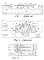
- FIGURES 1 and 2 are representative prior art microbridge MAF structures of this type as disclosed in patent 4,501,144 already cited above.
- the sensors and heater of this prior art device were described as being preferably fabricated of nickel-iron (permalloy) and these sensor and heater grids are encapsulated in a thin film of dielectric, typically comprising layers 28 and 29, preferably of silicon nitride. Air space 30 formed by selective etching of a depression in the monocrystalline silicon base 20 allows the elements 22, 24, and 26 to be surrounded by air. More detail of these prior art figures may be had by reference to patent 4,501,144.
- the MAF sensor utilizes the material platinum (in preferred thickness of 1000 angstroms or less) in the fabrication of the resistive elements 22, 24, and 26 although the invention is not in the use of platinum per se.
- platinum is preferred over permalloy.
- the poor adhesion of platinum to silicon nitride is a serious issue in this fabricating process.
- Platinum films greater than 4500 angstroms in thickness are said to be adherent to oxide-based ceramics in which the adhesion is said to be dependent on the rough surface of the ceramic, and on the presence of minor constituents in the ceramic, which is never a single compound.
- This roughness is on a scale of many microns up to thousandths of an inch, and would not be suitable for films in the 200 to 3500 angstrom range, for example, for which polished surfaces are required that have no discontinuities due to roughness.
- An objective of this invention is to provide an atomically smooth adhesion layer between the platinum metal sensor layer and the nitride substrate, such that roughness of the interface is not required.
- the layer of this invention must each satisfy two requirements: (1) it must form a strong bond to the platinum and to the silicon nitride, and (2) it must be physically stable against diffusion of its constituent atoms, or any impurities it may contain, into the platinum.
- Standard metallic adhesive films such as Cr or Ti:W alloy can interact with and diffuse into platinum at the elevated annealing temperatures to result in adhesion failure and to severely degrade properties such as TCR and resistance. If no adhesion promoter is used, widespread delamination, blistering and/or agglomeration will result during the necessary high temperature anneal.
- One of the known prior art microstructure gas flow sensors illustrates the limitations which are associated with using a standard chromium (Cr) metal adhesion film with a platinum sensor.
- This prior art device utilizes a chromium adhesion layer of about 50 angstroms beneath the thin film ( ⁇ 1000 angstroms) platinum resistor.
- the annealing temperatures are, of necessity, controlled to less than 400°C to avoid diffusion of chromium into the platinum, whereas platinum is not effectively stabilized with anneals less than about 500°C. If annealing temperatures were to exceed 400°C, a platinum/chromium interdiffusion takes place which severely degrades the platinum sensor properties, for example, by reducing the temperature coefficient of resistance (TCR) to less than half the value obtained by the use of this invention.
- TCR temperature coefficient of resistance
- DE-A-3603757 discloses a film resistor having a silicon substrate on which is a silicon oxide layer or a silicon nitride layer, then a titanium dioxide pattern layer and a platinum pattern layer. Formed on the platinum layer is a gold layer, then a second titanium dioxide layer and finally a top passivation layer of silicon dioxide.
- the passivation layer can be made of silicon nitride.
- GB-A-2181298 discloses a platinum resistance thermometer having an aluminium oxide layer of several thousand angstroms deposited on a silicon substrate and then a platinum film, again of several thousand angstroms, is deposited on the aluminium oxide layer.
- the present invention provides a thin film platinum on silicon nitride sensor structure comprising a layer of silicon nitride, a thin film layer of a metal oxide deposited on said silicon nitride surface, and a thin film of platinum deposited on said metal oxide layer, the structure characterised in that the metal oxide is selected from the group consisting of chromium oxide C r2 O3, tantalum oxide T a2 O5 and nickel oxide NiO.
- the present invention also provides a method of fabricating a platinum-based sensor on a silicon nitride base, the method comprising providing a silicon nitride layer, depositing a thin film layer of a metal oxide on said silicon nitride surface, depositing a thin film of platinum on said metal oxide layer, the method characterised in that the step of depositing the layer comprises depositing a layer of metal oxide selected from the group consisting of chromium oxide C r2 O3, tantalum oxide T a2 O5 and nickel oxide NiO.
- At least one metal oxide layer may have a thickness in the range of about 20 to 100 angstroms, advantageously 50 angstroms.
- the adhesion layer must be pure with respect to metallic impurities or excesses of the principal metal. This prevents diffusion of metal atoms from the adhesion layer into the platinum. This stability is particularly important for films of typical thickness of 1000 angstroms because a specified quantity of impurity atoms will have adverse electrical effects after the anneal that are in inverse proportion to the thickness of the platinum film.
- the oxide adhesion layer must be stable, and yet must have surface atoms that bond well to the platinum atoms. However, not all stable oxide layers adhere well. The oxygen surface atoms do not bond well, because platinum oxide is weakly bonded and decomposes at temperatures of the anneal. Therefore, it is the metallic component of the oxide that must form the strong bond.
- SiO2 is a good adhesion layer candidate, because some platinum silicides are stable above the anneal temperatures (PtSi is stable to 1100°C), however, SiO2 is not satisfactory. Si is not a metal, and in the absence of the actual silicide compound, the Pt/Si bond may not be of comparable strength to a Metal/Pt bond of a more generalized type.
- the common factor shared by the satisfactory, preferred metal oxide adhesion layer types is that the metal oxides are quite refractory. That this factor can be a requirement for a successful adhesion layer of this invention is supported by the argument that the oxide must be stable against decomposition which could release metal atoms to contaminate the platinum. We have not investigated all the available metal oxides. However, the following table lists the melting points of the refractory metal oxides which we have found to form adhesion layers which are strongly bonded to and do not contaminate the platinum. It is worthy to note that all of these oxides can be deposited by sputtering reactively in a suitable partial pressure of oxygen to ensure that no excess of metal atoms exists to diffuse into and to contaminate the platinum.
- a thin metal oxide intermediate layer i.e., chromium oxide (Cr2O3), aluminum oxide (Al2O3), tantalum oxide (Ta2O5), nickel oxide (Ni2O3) significantly improves the adhesion of the platinum sensor films on silicon nitride. Incorporation of this adhesion layer also minimizes the development of structural defects and sensor resistance variations which are otherwise encountered.
- One method of fabricating such oxide films makes use of electron beam evaporation of the oxide under high vacuum conditions. We have made satisfactory Al2O3 adhesion layers in this way. This method produces satisfactory adhesion layers, provided that steps are taken to insure correct stoichiometry of the metal oxides. This is necessary to prevent contamination of the platinum by excess metal migrating from the adhesion layer. Using electron beam evaporation, it is generally easier to maintain higher purity of the deposited films relative to sputtering. Purity may be an important consideration when attempting to reproducably obtain a high temperature coefficient of resistance.
- An alternate method is gas discharge sputter deposition with an oxygen component in the discharge gas. With sufficient excess oxygen the complete oxidation of the adhesion layer is assured.
- the following sensor layer processing sequence using sputter deposition is one which can be utilized in the fabrication of Pt sensors with significantly improved adhesion stability.
- RF sputtering as a method utilized for the deposition of the oxide adhesion layers and Pt sensor films.
- Inherent in most sputtering processes is the capability to backsputter, or sputter etch the substrates to remove surface contaminates and/or a thin ( ⁇ 100 ⁇ ) substrate surface layer to provide a clean base material for the subsequent depositions.
- this invention is not limited to the narrow processing area of sputtering, only. Electron beam evaporation, Ion beam deposition, etc., techniques can be utilized to deposit the oxide adhesion layers and Pt sensor films needed in the fabrication of Pt-based sensing devices. In situ substrate cleaning techniques can also be adapted to these other procedures, to provide a clean substrate surface for the subsequent depositions.
- FIGURES 1 and 2 disclose a prior art microbridge device for sensing mass air flow.
- FIGURE 3 shows a cross-section view of a portion of the structure according to the invention showing a chromium oxide embodiment of the adhesion layer.
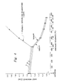
- FIGURE 4 graphs sheet resistance versus annealing temperature.
- a thin, non-reactive metal oxide such as Cr2O3, Ta2O5, Ni2O3
- a thin, non-reactive metal oxide such as Cr2O3, Ta2O5, Ni2O3
- This adhesion is continued through the high temperature anneals.
- incorporation of the thin oxide adhesion layer significantly minimizes the development of structural defects and results in markedly improved uniformity and control of platinum sensor/heater resistance properties.
- the oxide adhesion layer does not react with platinum to adversely influence the temperature coefficient of resistance (TCR) or cause undesired changes in resistance.
- TCR temperature coefficient of resistance
- the use of the oxide adhesion layer in the platinum sensor fabrication significantly improves the reliability.
- a silicon substrate 40 having on the surface 41 thereof a thin film of silicon nitride 42.
- the silicon nitride layer may be, for example, on the order of 5000 angstroms in thickness.
- Deposited on the surface 43 of the silicon nitride is a very thin (20-100 angstroms) layer of non-reactive metal oxide 44.
- Chromium (or chromic) oxide (Cr2O3) is one of many effective embodiments of the metal oxide adhesion layer.
- the thin layer of platinum 45 is then deposited over the Cr2O3 adhesion layer. This layer 45 may typically be on the order of 1000 angstroms in thickness, however the thickness may be varied widely depending on the model.
- a surface Cr2O3 adhesion layer 46 is also utilized to promote adhesion between platinum layer 45 and the encapsulation silicon nitride layer 47.
- the incorporation of a thin oxide film not only is an effective adhesion promoter for platinum on silicon nitride, but also minimizes the development of structural defects and the resultant non-uniform resistance which is observed in platinum-only (that is, no adhesion layer) films at elevated temperatures (500-700°C). Also, there are no apparent reactions between the metal oxide adhesion layer and the platinum and the TCR and resistance do not deteriorate as they do when atoms from metal adhesion layers diffuse into the platinum film.
- the thickness of the adhesion layer would not affect its adhesion properties once the thickness exceeded a critical value necessary to completely cover the silicon nitride substrate.
- the critical minimum thickness for good adhesion is about 20 angstroms, with a preferred thickness of about 50 angstroms.
- the 50 angstrom thickness though preferred, is not in any sense a limiting thickness, as other thicknesses will perform well.
- the oxides are reactively sputtered in the static mode from a metal target.
- the oxygen concentration is kept more than high enough to result in fully reacted material.
- Oxides of chromium, tantalum, and nickel were evaluated as adhesion promoting layers for platinum. All oxide films evaluated thus far effectively promote platinum adhesion and permit stabilization and property development anneals at elevated temperatures without deleterious chemical reactions and without the development of defects, delaminations, and uncontrolled resistance shifts that are evident in annealed platinum-only films.
- FIGURE 4 there is shown graphically a plot of the measured sheet resistance vs. annealing temperature for 1000 angstrom platinum films both with and without a metal oxide adhesion layer between the Si3N4 and the platinum film.
- curve A represents the results when platinum is deposited directly on the silicon nitride with no adhesion layer.
- Curve B represents the results when using an adhesion layer of tantalum oxide and Curve C when using an adhesion layer of nickel oxide. It can be seen that the curves track closely with each other at the lower annealing temperatures up to 450°C. Above that temperature, curve A has a discontinuity and breaks sharply upward with defects and delaminations of the platinum occurring. Successful annealing of the platinum with the tantalum oxide and with the nickel oxide adhesion layers was conducted up to 950°C.
Landscapes
- Physics & Mathematics (AREA)
- Engineering & Computer Science (AREA)
- Microelectronics & Electronic Packaging (AREA)
- Fluid Mechanics (AREA)
- General Physics & Mathematics (AREA)
- Electromagnetism (AREA)
- Investigating Or Analyzing Materials By The Use Of Fluid Adsorption Or Reactions (AREA)
- Measuring Oxygen Concentration In Cells (AREA)
- Adhesives Or Adhesive Processes (AREA)
- Measuring Volume Flow (AREA)
- Electroplating Methods And Accessories (AREA)
- Thermistors And Varistors (AREA)
Abstract
Description
- The field of this invention is air velocity or flow sensors, particularly of the general type called microbridge mass air flow (MAF) sensors as typified by the devices shown in such patents as 4,472,239; 4,478,076; 4,478,077; 4,501,144; 4,548,078; 4,566,320; 4,581,928; 4,624,137; 4,651,564; and 4,696,188, all assigned to the same assignee as the present invention.
- In microbridge sensors, thin platinum films of preferred thickness of 1000 angstroms must be strongly attached to an atomically smooth silicon nitride substrate, typically 5000 angstroms thick, on a polished silicon wafer surface. Without an intermediate adhesion layer between the nitride and the platinum, the attachment is weak, and fails to withstand annealing temperature stresses of 600°C or more that are required to give the platinum stable electrical characteristics.
- Metal adhesion layers are not satisfactory because, although some metals adhere satisfactorily to both the nitride and the platinum, all suitable refractory metals that have been investigated (including chromium, titanium, tungsten, nickel, iron, and tantalum) diffuse into the platinum during the anneal, and adversely change its electrical characteristics by increasing its resistivity and reducing its temperature coefficient.
- The invention specifies the use and the properties of a class of refractory metal oxide layers that do not have the disadvantages of metal or metal alloy layers.
- The flow sensors of this prior art generally comprise a pair of thin film heat sensors and a thin film heater. The flow sensors further comprise a semiconductor body with a depression therein and structure connecting the heater and the sensors to the body and bridging the depression so that at least the major portion of the heater and sensors are out of contact with the body. The sensors are disposed on opposite sides of the heater. The heater is operated above ambient temperature under both flow and no-flow conditions. FIGURES 1 and 2 are representative prior art microbridge MAF structures of this type as disclosed in patent 4,501,144 already cited above. Thus, there is disclosed a pair of thin
film heat sensors thin film heater 26, and asemiconductor base 20, preferably monocrystalline silicon, supporting the sensors and heater out of contact with the base. The sensors and heater of this prior art device were described as being preferably fabricated of nickel-iron (permalloy) and these sensor and heater grids are encapsulated in a thin film of dielectric, typically comprisinglayers Air space 30 formed by selective etching of a depression in themonocrystalline silicon base 20 allows theelements - In the present invention the MAF sensor utilizes the material platinum (in preferred thickness of 1000 angstroms or less) in the fabrication of the
resistive elements - The possibility of attaching platinum films to various oxide-based ceramics has been explored in "Thin Film PRTD platinum thin-film resistors as accurate and stable temperature sensors" (Measurement and Control, December 1982). Platinum films greater than 4500 angstroms in thickness are said to be adherent to oxide-based ceramics in which the adhesion is said to be dependent on the rough surface of the ceramic, and on the presence of minor constituents in the ceramic, which is never a single compound. This roughness is on a scale of many microns up to thousandths of an inch, and would not be suitable for films in the 200 to 3500 angstrom range, for example, for which polished surfaces are required that have no discontinuities due to roughness.
- An objective of this invention is to provide an atomically smooth adhesion layer between the platinum metal sensor layer and the nitride substrate, such that roughness of the interface is not required. The layer of this invention must each satisfy two requirements: (1) it must form a strong bond to the platinum and to the silicon nitride, and (2) it must be physically stable against diffusion of its constituent atoms, or any impurities it may contain, into the platinum.
- There is no problem with the attachment of the adhesion layer to the nitride. As we have determined experimentally, many non-noble metal oxides adhere well to the nitride substrate. The problem addressed by the invention is the reliable adherence of the adhesion layer to a platinum layer or to other noble metal layers without deterioration of the adhesion or the electrical properties during the anneal.
- Various metallic adhesion layers are known in the prior art such as Cr and Ti:W alloy, however, these materials are completely inadequate for use in this invention. Standard metallic adhesive films, such as Cr or Ti:W alloy can interact with and diffuse into platinum at the elevated annealing temperatures to result in adhesion failure and to severely degrade properties such as TCR and resistance. If no adhesion promoter is used, widespread delamination, blistering and/or agglomeration will result during the necessary high temperature anneal. One of the known prior art microstructure gas flow sensors illustrates the limitations which are associated with using a standard chromium (Cr) metal adhesion film with a platinum sensor. This prior art device utilizes a chromium adhesion layer of about 50 angstroms beneath the thin film (∼ 1000 angstroms) platinum resistor. With this arrangement, the annealing temperatures are, of necessity, controlled to less than 400°C to avoid diffusion of chromium into the platinum, whereas platinum is not effectively stabilized with anneals less than about 500°C. If annealing temperatures were to exceed 400°C, a platinum/chromium interdiffusion takes place which severely degrades the platinum sensor properties, for example, by reducing the temperature coefficient of resistance (TCR) to less than half the value obtained by the use of this invention.
- DE-A-3603757 discloses a film resistor having a silicon substrate on which is a silicon oxide layer or a silicon nitride layer, then a titanium dioxide pattern layer and a platinum pattern layer. Formed on the platinum layer is a gold layer, then a second titanium dioxide layer and finally a top passivation layer of silicon dioxide. In one variation, the passivation layer can be made of silicon nitride.
- GB-A-2181298 discloses a platinum resistance thermometer having an aluminium oxide layer of several thousand angstroms deposited on a silicon substrate and then a platinum film, again of several thousand angstroms, is deposited on the aluminium oxide layer.
- The present invention provides a thin film platinum on silicon nitride sensor structure comprising a layer of silicon nitride, a thin film layer of a metal oxide deposited on said silicon nitride surface, and a thin film of platinum deposited on said metal oxide layer, the structure characterised in that the metal oxide is selected from the group consisting of chromium oxide Cr2O₃, tantalum oxide Ta2O₅ and nickel oxide NiO.
- The present invention also provides a method of fabricating a platinum-based sensor on a silicon nitride base, the method comprising providing a silicon nitride layer, depositing a thin film layer of a metal oxide on said silicon nitride surface, depositing a thin film of platinum on said metal oxide layer, the method characterised in that the step of depositing the layer comprises depositing a layer of metal oxide selected from the group consisting of chromium oxide Cr2O₃, tantalum oxide Ta2O₅ and nickel oxide NiO.
- At least one metal oxide layer may have a thickness in the range of about 20 to 100 angstroms, advantageously 50 angstroms.
- The adhesion layer must be pure with respect to metallic impurities or excesses of the principal metal. This prevents diffusion of metal atoms from the adhesion layer into the platinum. This stability is particularly important for films of typical thickness of 1000 angstroms because a specified quantity of impurity atoms will have adverse electrical effects after the anneal that are in inverse proportion to the thickness of the platinum film. The oxide adhesion layer must be stable, and yet must have surface atoms that bond well to the platinum atoms. However, not all stable oxide layers adhere well. The oxygen surface atoms do not bond well, because platinum oxide is weakly bonded and decomposes at temperatures of the anneal. Therefore, it is the metallic component of the oxide that must form the strong bond. We have tried silicon dioxide and one might expect SiO₂ to be a good adhesion layer candidate, because some platinum silicides are stable above the anneal temperatures (PtSi is stable to 1100°C), however, SiO₂ is not satisfactory. Si is not a metal, and in the absence of the actual silicide compound, the Pt/Si bond may not be of comparable strength to a Metal/Pt bond of a more generalized type.
- The common factor shared by the satisfactory, preferred metal oxide adhesion layer types is that the metal oxides are quite refractory. That this factor can be a requirement for a successful adhesion layer of this invention is supported by the argument that the oxide must be stable against decomposition which could release metal atoms to contaminate the platinum. We have not investigated all the available metal oxides. However, the following table lists the melting points of the refractory metal oxides which we have found to form adhesion layers which are strongly bonded to and do not contaminate the platinum. It is worthy to note that all of these oxides can be deposited by sputtering reactively in a suitable partial pressure of oxygen to ensure that no excess of metal atoms exists to diffuse into and to contaminate the platinum.

- In this invention, the use of a thin metal oxide intermediate layer, i.e., chromium oxide (Cr₂O₃), aluminum oxide (Al₂O₃), tantalum oxide (Ta₂O₅), nickel oxide (Ni₂O₃) significantly improves the adhesion of the platinum sensor films on silicon nitride. Incorporation of this adhesion layer also minimizes the development of structural defects and sensor resistance variations which are otherwise encountered.
- One method of fabricating such oxide films makes use of electron beam evaporation of the oxide under high vacuum conditions. We have made satisfactory Al₂O₃ adhesion layers in this way. This method produces satisfactory adhesion layers, provided that steps are taken to insure correct stoichiometry of the metal oxides. This is necessary to prevent contamination of the platinum by excess metal migrating from the adhesion layer. Using electron beam evaporation, it is generally easier to maintain higher purity of the deposited films relative to sputtering. Purity may be an important consideration when attempting to reproducably obtain a high temperature coefficient of resistance.
- An alternate method is gas discharge sputter deposition with an oxygen component in the discharge gas. With sufficient excess oxygen the complete oxidation of the adhesion layer is assured. The following sensor layer processing sequence using sputter deposition is one which can be utilized in the fabrication of Pt sensors with significantly improved adhesion stability.

- The examples referred to in this disclosure describe RF sputtering as a method utilized for the deposition of the oxide adhesion layers and Pt sensor films.
- Inherent in most sputtering processes is the capability to backsputter, or sputter etch the substrates to remove surface contaminates and/or a thin (<100 Å) substrate surface layer to provide a clean base material for the subsequent depositions.
- However, this invention is not limited to the narrow processing area of sputtering, only. Electron beam evaporation, Ion beam deposition, etc., techniques can be utilized to deposit the oxide adhesion layers and Pt sensor films needed in the fabrication of Pt-based sensing devices. In situ substrate cleaning techniques can also be adapted to these other procedures, to provide a clean substrate surface for the subsequent depositions.
- FIGURES 1 and 2 disclose a prior art microbridge device for sensing mass air flow.
- FIGURE 3 shows a cross-section view of a portion of the structure according to the invention showing a chromium oxide embodiment of the adhesion layer.
- FIGURE 4 graphs sheet resistance versus annealing temperature.
- The marginal adhesion of platinum to silicon nitride is a serious issue in the fabrication of platinum based sensors. High temperature anneals, that is, 500-1000°C, are required to develop the properties and stability necessary for effective device performance. The necessary annealing process, however, accentuates the problem of the already poor platinum to silicon nitride adhesion. These anneals are necessary to develop the device sensitivity, stability, and reliability needed for meeting device specifications.
- The use of a thin, non-reactive metal oxide (such as Cr₂O₃, Ta₂O₅, Ni₂O₃) adhesion layer in the thickness range of 20 to 100 angstroms, is very effective in enhancing and maintaining platinum adhesion to silicon nitride. This adhesion is continued through the high temperature anneals. Moreover, incorporation of the thin oxide adhesion layer significantly minimizes the development of structural defects and results in markedly improved uniformity and control of platinum sensor/heater resistance properties.
- The oxide adhesion layer does not react with platinum to adversely influence the temperature coefficient of resistance (TCR) or cause undesired changes in resistance. Thus, the use of the oxide adhesion layer in the platinum sensor fabrication significantly improves the reliability.
- Referring now to FIGURE 3, there is shown a
silicon substrate 40 having on thesurface 41 thereof a thin film ofsilicon nitride 42. The silicon nitride layer may be, for example, on the order of 5000 angstroms in thickness. Deposited on thesurface 43 of the silicon nitride is a very thin (20-100 angstroms) layer ofnon-reactive metal oxide 44. Chromium (or chromic) oxide (Cr₂O₃) is one of many effective embodiments of the metal oxide adhesion layer. The thin layer ofplatinum 45 is then deposited over the Cr₂O₃ adhesion layer. Thislayer 45 may typically be on the order of 1000 angstroms in thickness, however the thickness may be varied widely depending on the model. A surfaceCr₂O₃ adhesion layer 46 is also utilized to promote adhesion betweenplatinum layer 45 and the encapsulationsilicon nitride layer 47. The incorporation of a thin oxide film, not only is an effective adhesion promoter for platinum on silicon nitride, but also minimizes the development of structural defects and the resultant non-uniform resistance which is observed in platinum-only (that is, no adhesion layer) films at elevated temperatures (500-700°C). Also, there are no apparent reactions between the metal oxide adhesion layer and the platinum and the TCR and resistance do not deteriorate as they do when atoms from metal adhesion layers diffuse into the platinum film. - It would be expected that the thickness of the adhesion layer would not affect its adhesion properties once the thickness exceeded a critical value necessary to completely cover the silicon nitride substrate. In extensive experiments with chrome oxide adhesion layers, we have found that the critical minimum thickness for good adhesion is about 20 angstroms, with a preferred thickness of about 50 angstroms. The 50 angstrom thickness, though preferred, is not in any sense a limiting thickness, as other thicknesses will perform well. We have not defined the thickness effect for nickel oxide or tantalum oxide, but the initial experiments with both oxides have given very good quality adhesion and electrical characteristics of the platinum even for anneals as high as 950°C with the preferred 50 angstrom thick adhesion layers.
- In the deposition of the metal oxide adhesion layers, the oxides are reactively sputtered in the static mode from a metal target. The oxygen concentration is kept more than high enough to result in fully reacted material.
- Oxides of chromium, tantalum, and nickel were evaluated as adhesion promoting layers for platinum. All oxide films evaluated thus far effectively promote platinum adhesion and permit stabilization and property development anneals at elevated temperatures without deleterious chemical reactions and without the development of defects, delaminations, and uncontrolled resistance shifts that are evident in annealed platinum-only films.
- In FIGURE 4, there is shown graphically a plot of the measured sheet resistance vs. annealing temperature for 1000 angstrom platinum films both with and without a metal oxide adhesion layer between the Si₃N₄ and the platinum film. Three curves are shown on this graph, curve A represents the results when platinum is deposited directly on the silicon nitride with no adhesion layer. Curve B represents the results when using an adhesion layer of tantalum oxide and Curve C when using an adhesion layer of nickel oxide. It can be seen that the curves track closely with each other at the lower annealing temperatures up to 450°C. Above that temperature, curve A has a discontinuity and breaks sharply upward with defects and delaminations of the platinum occurring. Successful annealing of the platinum with the tantalum oxide and with the nickel oxide adhesion layers was conducted up to 950°C.
Claims (10)
- A thin film platinum on silicon nitride sensor structure comprising a layer of silicon nitride (42), a thin film layer (44) of a metal oxide deposited on said silicon nitride surface, and a thin film of platinum (45) deposited on said metal oxide layer, the structure characterised in that the metal oxide is selected from the group consisting of chromium oxide Cr2O₃, tantalum oxide Ta2O₅ and nickel oxide NiO.
- A structure according to Claim 1 characterised by:
a substrate of silicon (40) on which the layer of silicon nitride is deposited;
a second thin film layer of metal oxide (46) over said platinum; and
a passivating silicon nitride layer (42) over said second metal oxide layer and said platinum layer. - A structure according to any preceding Claim characterised in that at least one metal oxide layer has a thickness in the range of about 20 to 100 angstroms.
- A structure according to any preceding Claim characterised in that at least one metal oxide layer has a thickness of the order of 50 angstroms.
- A structure according to any preceding Claim characterised in that the thin film layer(s) of metal oxide and of platinum are sputter depositions.
- A method of fabricating a platinum-based sensor on a silicon nitride base, the method comprising:
providing a silicon nitride layer (42),
depositing a thin film layer (44) of a metal oxide on said silicon nitride surface,
depositing a thin film of platinum (45) on said metal oxide layer, the method characterised in that the step of depositing the layer comprises depositing a layer of metal oxide selected from the group consisting of chromium oxide Cr2O₃, tantalum oxide Ta2O₅ and nickel oxide NiO. - A method according to Claim 6 characterised by providing a substrate of silicon (4) on which the layer of silicon nitride (42) is deposited, depositing a second thin film layer (46) of metal oxide over the platinum and depositing a passivating silicon nitride layer (47) over said second metal oxide layer and said platinum layer.
- A method according to Claim 6 or 7 characterised in that the step(s) of depositing metal oxide and the step of depositing platinum are by sputter deposition.
- A method according to any of Claims 6 to 8 characterised in that the depositing of at least one metal oxide layer is to a thickness in the range of about 20 - 100 angstroms.
- A method according to any of Claims 6 to 9 characterised in that the depositing of at least one metal oxide layer is to a thickness of the order of 50 angstroms.
Applications Claiming Priority (2)
| Application Number | Priority Date | Filing Date | Title |
|---|---|---|---|
| US07/289,098 US4952904A (en) | 1988-12-23 | 1988-12-23 | Adhesion layer for platinum based sensors |
| US289098 | 2002-11-06 |
Publications (3)
| Publication Number | Publication Date |
|---|---|
| EP0375399A2 EP0375399A2 (en) | 1990-06-27 |
| EP0375399A3 EP0375399A3 (en) | 1990-09-19 |
| EP0375399B1 true EP0375399B1 (en) | 1995-09-06 |
Family
ID=23110052
Family Applications (1)
| Application Number | Title | Priority Date | Filing Date |
|---|---|---|---|
| EP89313358A Expired - Lifetime EP0375399B1 (en) | 1988-12-23 | 1989-12-20 | Adhesion layer for platinum based sensors |
Country Status (6)
| Country | Link |
|---|---|
| US (1) | US4952904A (en) |
| EP (1) | EP0375399B1 (en) |
| JP (1) | JPH02226017A (en) |
| AT (1) | ATE127583T1 (en) |
| CA (1) | CA2000030A1 (en) |
| DE (1) | DE68924140T2 (en) |
Families Citing this family (70)
| Publication number | Priority date | Publication date | Assignee | Title |
|---|---|---|---|---|
| US5164999A (en) * | 1991-05-20 | 1992-11-17 | Johnson Matthey, Inc. | Blackbody fired on silica fiber |
| US5201022A (en) * | 1991-05-20 | 1993-04-06 | Johnson Matthey Inc. | Coated optical fiber |
| US5235312A (en) * | 1991-11-18 | 1993-08-10 | Micron Technology, Inc. | Polysilicon resistors and methods of fabrication |
| US5323138A (en) * | 1992-09-04 | 1994-06-21 | Trw Inc. | Reliable thin film resistors for integrated circuit applications |
| US5587130A (en) * | 1993-03-15 | 1996-12-24 | Arizona Board Of Regents | Selected area adhesion and surface passivation of metal films |
| US5468672A (en) * | 1993-06-29 | 1995-11-21 | Raytheon Company | Thin film resistor and method of fabrication |
| AT404758B (en) * | 1993-07-29 | 1999-02-25 | Urban Gerald Dipl Ing Dr | Miniature probe, process for its production and its use |
| US5439840A (en) * | 1993-08-02 | 1995-08-08 | Motorola, Inc. | Method of forming a nonvolatile random access memory capacitor cell having a metal-oxide dielectric |
| US5510013A (en) * | 1993-09-10 | 1996-04-23 | Robert Bosch Gmbh | Layer system for electrochemical probes |
| JP3333948B2 (en) * | 1994-02-23 | 2002-10-15 | 本田技研工業株式会社 | Manufacturing method of gas type sensor |
| DE19511590A1 (en) * | 1995-03-29 | 1996-10-02 | Bosch Gmbh Robert | Measurement element for flow sensor with diaphragm, heater and temp. sensor |
| KR100214267B1 (en) * | 1995-04-07 | 1999-08-02 | 김영환 | Semiconductor device fabrication method |
| DE19601592C1 (en) * | 1996-01-18 | 1997-05-07 | Bosch Gmbh Robert | Sensor containing platinum silicide bond layer |
| DE19605180A1 (en) * | 1996-02-13 | 1997-08-14 | Daimler Benz Ag | Anemometer, measuring correct plus or minus sign |
| US5759493A (en) * | 1996-04-30 | 1998-06-02 | Arizona Instrument Corporation | Apparatus for detecting a specified gas within a mixture |
| KR100214269B1 (en) * | 1996-06-27 | 1999-08-02 | 김영환 | Method for forming passivation layer of semiconductor device |
| US6025205A (en) * | 1997-01-07 | 2000-02-15 | Tong Yang Cement Corporation | Apparatus and methods of forming preferred orientation-controlled platinum films using nitrogen |
| US6054331A (en) * | 1997-01-15 | 2000-04-25 | Tong Yang Cement Corporation | Apparatus and methods of depositing a platinum film with anti-oxidizing function over a substrate |
| JP3457826B2 (en) * | 1997-01-31 | 2003-10-20 | 株式会社リコー | Thin film resistor and method of manufacturing the same, flow sensor, humidity sensor, gas sensor, temperature sensor |
| US5958606A (en) * | 1997-02-05 | 1999-09-28 | Cyntec Company | Substrate structure with adhesive anchoring-seams for securely attaching and boding to a thin film supported thereon |
| DE19710559A1 (en) * | 1997-03-14 | 1998-09-17 | Bosch Gmbh Robert | Sensor especially mass flow sensor |
| US6498097B1 (en) | 1997-05-06 | 2002-12-24 | Tong Yang Cement Corporation | Apparatus and method of forming preferred orientation-controlled platinum film using oxygen |
| US5910880A (en) * | 1997-08-20 | 1999-06-08 | Micron Technology, Inc. | Semiconductor circuit components and capacitors |
| DE19744228C1 (en) * | 1997-10-07 | 1998-11-26 | Bosch Gmbh Robert | Mass flow sensor with membrane and attached resistance element |
| DE19806211C2 (en) * | 1998-02-16 | 2000-11-02 | Bosch Gmbh Robert | Thin-film sensor |
| US6162744A (en) * | 1998-02-28 | 2000-12-19 | Micron Technology, Inc. | Method of forming capacitors having high-K oxygen containing capacitor dielectric layers, method of processing high-K oxygen containing dielectric layers, method of forming a DRAM cell having having high-K oxygen containing capacitor dielectric layers |
| US6191443B1 (en) | 1998-02-28 | 2001-02-20 | Micron Technology, Inc. | Capacitors, methods of forming capacitors, and DRAM memory cells |
| US6016686A (en) * | 1998-03-16 | 2000-01-25 | Lockheed Martin Energy Research Corporation | Micromechanical potentiometric sensors |
| US6730559B2 (en) * | 1998-04-10 | 2004-05-04 | Micron Technology, Inc. | Capacitors and methods of forming capacitors |
| US6156638A (en) | 1998-04-10 | 2000-12-05 | Micron Technology, Inc. | Integrated circuitry and method of restricting diffusion from one material to another |
| US6165834A (en) * | 1998-05-07 | 2000-12-26 | Micron Technology, Inc. | Method of forming capacitors, method of processing dielectric layers, method of forming a DRAM cell |
| US6255186B1 (en) | 1998-05-21 | 2001-07-03 | Micron Technology, Inc. | Methods of forming integrated circuitry and capacitors having a capacitor electrode having a base and a pair of walls projecting upwardly therefrom |
| JP3606095B2 (en) * | 1998-10-06 | 2005-01-05 | セイコーエプソン株式会社 | Manufacturing method of semiconductor device |
| DE19901183C2 (en) * | 1999-01-14 | 2001-01-25 | Sensotherm Temperatursensorik | Platinum temperature sensor and manufacturing method for the same |
| DE19901184C1 (en) * | 1999-01-14 | 2000-10-26 | Sensotherm Temperatursensorik | Platinum temperature sensor and method of manufacturing the same |
| US6369452B1 (en) | 1999-07-27 | 2002-04-09 | International Business Machines Corporation | Cap attach surface modification for improved adhesion |
| DE19951595A1 (en) * | 1999-10-27 | 2001-05-17 | Bosch Gmbh Robert | Mass flow sensor comprises a frame formed partially by silicon, metal layer, heating element, temperature measuring element and a membrane having a dielectric and/or non-conducting accommodating layer |
| US6331678B1 (en) | 1999-10-29 | 2001-12-18 | Agilent Technologies, Inc. | Reduction of blistering and delamination of high-temperature devices with metal film |
| US7005695B1 (en) | 2000-02-23 | 2006-02-28 | Micron Technology, Inc. | Integrated circuitry including a capacitor with an amorphous and a crystalline high K capacitor dielectric region |
| US7214295B2 (en) * | 2001-04-09 | 2007-05-08 | Vishay Dale Electronics, Inc. | Method for tantalum pentoxide moisture barrier in film resistors |
| JP5138134B2 (en) * | 2001-07-16 | 2013-02-06 | 株式会社デンソー | Thin film type sensor manufacturing method and flow sensor manufacturing method |
| JP4686922B2 (en) * | 2001-07-19 | 2011-05-25 | 株式会社デンソー | Manufacturing method of flow sensor |
| EP1622085A1 (en) * | 2004-07-19 | 2006-02-01 | Deutsches Krebsforschungszentrum | Method of producing x-ray computer tomography images from limited data of an image object |
| JP5108234B2 (en) * | 2005-02-07 | 2012-12-26 | 日本特殊陶業株式会社 | Micro heater and sensor |
| JP4966526B2 (en) * | 2005-09-07 | 2012-07-04 | 日立オートモティブシステムズ株式会社 | Flow sensor |
| WO2007091686A1 (en) * | 2006-02-09 | 2007-08-16 | Mitsui Mining & Smelting Co., Ltd. | Laminate, thin film sensor, thin film sensor module, and method for manufacturing the thin film sensor |
| US20100245030A1 (en) * | 2006-03-28 | 2010-09-30 | Mitsui Mining & Smelting Co., Ltd. | Processes for Producing Thin-Film Sensors, Thin-Film Sensors and Thin-Film Sensor Modules |
| US7782569B2 (en) * | 2007-01-18 | 2010-08-24 | Sae Magnetics (Hk) Ltd. | Magnetic recording head and media comprising aluminum oxynitride underlayer and a diamond-like carbon overcoat |
| US8014104B2 (en) * | 2007-03-21 | 2011-09-06 | Sae Magnetics (Hk) Ltd. | Magnetic head/disk with transition metal oxynitride adhesion/corrosion barrier and diamond-like carbon overcoat bilayer |
| US8646311B1 (en) | 2007-11-09 | 2014-02-11 | Atmospheric Sensors Ltd. | Sensors for hydrogen, ammonia |
| US8039314B2 (en) * | 2008-08-04 | 2011-10-18 | International Business Machines Corporation | Metal adhesion by induced surface roughness |
| TWI514608B (en) * | 2010-01-14 | 2015-12-21 | Dow Global Technologies Llc | Moisture resistant photovoltaic devices with exposed conductive grid |
| US9059349B2 (en) * | 2010-02-09 | 2015-06-16 | Dow Global Technologies Llc | Moisture resistant photovoltaic devices with improved adhesion of barrier film |
| US8356514B2 (en) | 2011-01-13 | 2013-01-22 | Honeywell International Inc. | Sensor with improved thermal stability |
| US9664572B2 (en) * | 2012-11-28 | 2017-05-30 | Seagate Technology Llc | Thin films having large temperature coefficient of resistance and methods of fabricating same |
| DE102013016331A1 (en) | 2013-10-05 | 2015-04-09 | Micronas Gmbh | layer system |
| DE102013016330A1 (en) | 2013-10-05 | 2015-04-09 | Micronas Gmbh | layer system |
| US9612146B2 (en) | 2014-02-07 | 2017-04-04 | Honeywell International, Inc. | Airflow sensor with dust reduction |
| RU2583952C1 (en) * | 2015-01-26 | 2016-05-10 | Открытое акционерное общество "Научно-производственное объединение "ЭРКОН" (ОАО "НПО "ЭРКОН") | Method for producing thin film resistor |
| US10530329B2 (en) | 2016-01-22 | 2020-01-07 | Qorvo Us, Inc. | Guided wave devices with selectively thinned piezoelectric layers |
| US10938367B2 (en) | 2016-03-31 | 2021-03-02 | Qorvo Us, Inc. | Solidly mounted layer thin film device with grounding layer |
| DE102016208970A1 (en) | 2016-05-24 | 2017-11-30 | Robert Bosch Gmbh | A method of making an electromigration resistant crystalline transition metal silicide layer, corresponding layer sequence, and microheater |
| US11262250B2 (en) * | 2018-02-28 | 2022-03-01 | Applied Materials, Inc. | Method for measuring a temperature |
| KR102170210B1 (en) * | 2018-12-20 | 2020-10-28 | 세종공업 주식회사 | High temperature environment stabilization process of platinum detection sensor |
| US20220365014A1 (en) * | 2019-10-24 | 2022-11-17 | University Of Louisville Research Foundation, Inc. | Microfabricated differential scanning calorimetry system and methods of use thereof |
| US11835529B1 (en) | 2019-10-24 | 2023-12-05 | University Of Louisville Research Foundation, Inc. | Plasma thermograms for diagnosis and treatment of acute myocardial infarction |
| RU2736630C1 (en) * | 2020-02-10 | 2020-11-19 | Открытое акционерное общество "Авангард" | Thin-film platinum thermistor on glass substrate and method of manufacturing thereof |
| CN112880852B (en) * | 2021-01-07 | 2023-02-24 | 上海交通大学 | High-temperature platinum film resistor temperature sensor and preparation method thereof |
| WO2023288108A1 (en) * | 2021-07-16 | 2023-01-19 | The University Of Chicago | Biocompatible surface for quantum sensing and methods thereof |
| CN115219056B (en) * | 2022-07-18 | 2024-09-03 | 山东大学 | Film type temperature sensor with quick response and high temperature resistance and preparation method thereof |
Family Cites Families (7)
| Publication number | Priority date | Publication date | Assignee | Title |
|---|---|---|---|---|
| US4234405A (en) * | 1971-09-16 | 1980-11-18 | Imperial Chemical Industries Limited | Electrode for electrochemical processes |
| US4525223A (en) * | 1978-09-19 | 1985-06-25 | Noboru Tsuya | Method of manufacturing a thin ribbon wafer of semiconductor material |
| US4624137A (en) * | 1981-10-09 | 1986-11-25 | Honeywell Inc. | Semiconductor device |
| US4471405A (en) * | 1981-12-28 | 1984-09-11 | International Business Machines Corporation | Thin film capacitor with a dual bottom electrode structure |
| US4423087A (en) * | 1981-12-28 | 1983-12-27 | International Business Machines Corporation | Thin film capacitor with a dual bottom electrode structure |
| JPS61188901A (en) * | 1985-02-16 | 1986-08-22 | 株式会社日本自動車部品総合研究所 | Membrane type resistance for flow rate sensor |
| DE3630393C2 (en) * | 1985-09-10 | 1994-06-23 | Sharp Kk | Resistance thermometer |
-
1988
- 1988-12-23 US US07/289,098 patent/US4952904A/en not_active Expired - Fee Related
-
1989
- 1989-10-02 CA CA002000030A patent/CA2000030A1/en not_active Abandoned
- 1989-12-20 AT AT89313358T patent/ATE127583T1/en active
- 1989-12-20 EP EP89313358A patent/EP0375399B1/en not_active Expired - Lifetime
- 1989-12-20 DE DE68924140T patent/DE68924140T2/en not_active Expired - Fee Related
- 1989-12-22 JP JP1334593A patent/JPH02226017A/en active Pending
Non-Patent Citations (1)
| Title |
|---|
| I.E.E.E. TRANSACTIONS ON ELECTRON DEVICES, vol. ED-34, no. 12, part I of 2 parts, December 1987, New York, US; O. TABATA et al.: "Monolithic Pressure-Flow Sensor" * |
Also Published As
| Publication number | Publication date |
|---|---|
| ATE127583T1 (en) | 1995-09-15 |
| EP0375399A3 (en) | 1990-09-19 |
| CA2000030A1 (en) | 1990-06-23 |
| EP0375399A2 (en) | 1990-06-27 |
| JPH02226017A (en) | 1990-09-07 |
| DE68924140T2 (en) | 1996-05-09 |
| DE68924140D1 (en) | 1995-10-12 |
| US4952904A (en) | 1990-08-28 |
Similar Documents
| Publication | Publication Date | Title |
|---|---|---|
| EP0375399B1 (en) | Adhesion layer for platinum based sensors | |
| US5006421A (en) | Metalization systems for heater/sensor elements | |
| US4462018A (en) | Semiconductor strain gauge with integral compensation resistors | |
| US4805296A (en) | Method of manufacturing platinum resistance thermometer | |
| JPH0819516B2 (en) | Method and structure for forming thin film alpha Ta | |
| KR100450919B1 (en) | Sensor and its manufacturing method | |
| KR100393945B1 (en) | Method for manufactuing a metal thin film resistor device and method for manufacturing a metal thin film temperature sensor using the same | |
| EP0069253A1 (en) | Thermal flow rate sensor | |
| US4649365A (en) | Platinum resistor for the measurement of temperatures | |
| KR19980080155A (en) | Sensor with thin film member | |
| JP3385087B2 (en) | Pt thin film integrated with substrate, thin film heater using the same, temperature detecting element and gas sensor | |
| JP2001057358A (en) | Method of fabricating sensor with thin film | |
| JPH0666162B2 (en) | Thin film resistor for strain gauge | |
| US4823073A (en) | Sensor for measuring the current or voltage of electrically conductive layers present on a reference substrate | |
| KR200156459Y1 (en) | Ntc thermistor | |
| AU4496200A (en) | Self-compensated ceramic strain gage for use at high temperatures | |
| EP4350313A1 (en) | Strain resistance film, physical quantity sensor, and method for manufacturing the strain resistance film | |
| Arshak et al. | Characterisation of a thin-film/thick-film strain gauge sensor on stainless steel | |
| JPH06213613A (en) | Distortion resistance material and manufacture thereof and thin film distortion sensor | |
| JP2002503805A (en) | Sensor with thin film design | |
| JPH01286470A (en) | Manufacture of semiconductor pressure sensor | |
| Bäther et al. | The effect of surfaces and interfaces on the properties of thin film resistors in the Cr Si/Al system | |
| JPH07263208A (en) | Thin film resistance for measurement and its manufacture | |
| JPH06231909A (en) | Resistor and its manufacture | |
| JPS63209103A (en) | Temperature sensor |
Legal Events
| Date | Code | Title | Description |
|---|---|---|---|
| PUAI | Public reference made under article 153(3) epc to a published international application that has entered the european phase |
Free format text: ORIGINAL CODE: 0009012 |
|
| AK | Designated contracting states |
Kind code of ref document: A2 Designated state(s): AT BE CH DE ES FR GB IT LI NL |
|
| PUAL | Search report despatched |
Free format text: ORIGINAL CODE: 0009013 |
|
| AK | Designated contracting states |
Kind code of ref document: A3 Designated state(s): AT BE CH DE ES FR GB IT LI NL |
|
| 17P | Request for examination filed |
Effective date: 19910318 |
|
| 17Q | First examination report despatched |
Effective date: 19930519 |
|
| GRAA | (expected) grant |
Free format text: ORIGINAL CODE: 0009210 |
|
| AK | Designated contracting states |
Kind code of ref document: B1 Designated state(s): AT BE CH DE ES FR GB IT LI NL |
|
| PG25 | Lapsed in a contracting state [announced via postgrant information from national office to epo] |
Ref country code: IT Free format text: LAPSE BECAUSE OF FAILURE TO SUBMIT A TRANSLATION OF THE DESCRIPTION OR TO PAY THE FEE WITHIN THE PRE;WARNING: LAPSES OF ITALIAN PATENTS WITH EFFECTIVE DATE BEFORE 2007 MAY HAVE OCCURRED AT ANY TIME BEFORE 2007. THE CORRECT EFFECTIVE DATE MAY BE DIFFERENT FROM THE ONE RECORDED.SCRIBED TIME-LIMIT Effective date: 19950906 Ref country code: AT Effective date: 19950906 Ref country code: ES Free format text: THE PATENT HAS BEEN ANNULLED BY A DECISION OF A NATIONAL AUTHORITY Effective date: 19950906 Ref country code: BE Effective date: 19950906 Ref country code: NL Free format text: LAPSE BECAUSE OF NON-PAYMENT OF DUE FEES Effective date: 19950906 |
|
| REF | Corresponds to: |
Ref document number: 127583 Country of ref document: AT Date of ref document: 19950915 Kind code of ref document: T |
|
| PGFP | Annual fee paid to national office [announced via postgrant information from national office to epo] |
Ref country code: FR Payment date: 19950918 Year of fee payment: 7 |
|
| PGFP | Annual fee paid to national office [announced via postgrant information from national office to epo] |
Ref country code: DE Payment date: 19950923 Year of fee payment: 7 |
|
| PGFP | Annual fee paid to national office [announced via postgrant information from national office to epo] |
Ref country code: GB Payment date: 19950926 Year of fee payment: 7 |
|
| REF | Corresponds to: |
Ref document number: 68924140 Country of ref document: DE Date of ref document: 19951012 |
|
| ET | Fr: translation filed | ||
| PGFP | Annual fee paid to national office [announced via postgrant information from national office to epo] |
Ref country code: CH Payment date: 19951231 Year of fee payment: 7 |
|
| NLV1 | Nl: lapsed or annulled due to failure to fulfill the requirements of art. 29p and 29m of the patents act | ||
| REG | Reference to a national code |
Ref country code: CH Ref legal event code: PL |
|
| PLBI | Opposition filed |
Free format text: ORIGINAL CODE: 0009260 |
|
| PLBF | Reply of patent proprietor to notice(s) of opposition |
Free format text: ORIGINAL CODE: EPIDOS OBSO |
|
| 26 | Opposition filed |
Opponent name: ROBERT BOSCH GMBH Effective date: 19960605 |
|
| PG25 | Lapsed in a contracting state [announced via postgrant information from national office to epo] |
Ref country code: GB Effective date: 19961220 |
|
| PG25 | Lapsed in a contracting state [announced via postgrant information from national office to epo] |
Ref country code: LI Free format text: LAPSE BECAUSE OF FAILURE TO SUBMIT A TRANSLATION OF THE DESCRIPTION OR TO PAY THE FEE WITHIN THE PRESCRIBED TIME-LIMIT Effective date: 19961231 Ref country code: CH Free format text: LAPSE BECAUSE OF FAILURE TO SUBMIT A TRANSLATION OF THE DESCRIPTION OR TO PAY THE FEE WITHIN THE PRESCRIBED TIME-LIMIT Effective date: 19961231 |
|
| GBPC | Gb: european patent ceased through non-payment of renewal fee |
Effective date: 19961220 |
|
| PG25 | Lapsed in a contracting state [announced via postgrant information from national office to epo] |
Ref country code: FR Effective date: 19970829 |
|
| PG25 | Lapsed in a contracting state [announced via postgrant information from national office to epo] |
Ref country code: DE Effective date: 19970902 |
|
| REG | Reference to a national code |
Ref country code: FR Ref legal event code: ST |
|
| PLBL | Opposition procedure terminated |
Free format text: ORIGINAL CODE: EPIDOS OPPC |
|
| PLBM | Termination of opposition procedure: date of legal effect published |
Free format text: ORIGINAL CODE: 0009276 |
|
| STAA | Information on the status of an ep patent application or granted ep patent |
Free format text: STATUS: OPPOSITION PROCEDURE CLOSED |
|
| 27C | Opposition proceedings terminated |
Effective date: 20020902 |