EP0372201B1 - Verfahren zum Abrufen von potentiell ungültigen Daten in einem Mehrrechnersystem - Google Patents
Verfahren zum Abrufen von potentiell ungültigen Daten in einem Mehrrechnersystem Download PDFInfo
- Publication number
- EP0372201B1 EP0372201B1 EP89119148A EP89119148A EP0372201B1 EP 0372201 B1 EP0372201 B1 EP 0372201B1 EP 89119148 A EP89119148 A EP 89119148A EP 89119148 A EP89119148 A EP 89119148A EP 0372201 B1 EP0372201 B1 EP 0372201B1
- Authority
- EP
- European Patent Office
- Prior art keywords
- line
- cache
- sce
- store
- state
- Prior art date
- Legal status (The legal status is an assumption and is not a legal conclusion. Google has not performed a legal analysis and makes no representation as to the accuracy of the status listed.)
- Expired - Lifetime
Links
Images


Classifications
-
- G—PHYSICS
- G06—COMPUTING; CALCULATING OR COUNTING
- G06F—ELECTRIC DIGITAL DATA PROCESSING
- G06F12/00—Accessing, addressing or allocating within memory systems or architectures
- G06F12/02—Addressing or allocation; Relocation
- G06F12/08—Addressing or allocation; Relocation in hierarchically structured memory systems, e.g. virtual memory systems
- G06F12/0802—Addressing of a memory level in which the access to the desired data or data block requires associative addressing means, e.g. caches
- G06F12/0806—Multiuser, multiprocessor or multiprocessing cache systems
- G06F12/0815—Cache consistency protocols
- G06F12/0817—Cache consistency protocols using directory methods
- G06F12/0822—Copy directories
Definitions
- the invention relates generally to caches in a multiprocessor environment and more particularly to a method for fetching lines of data from a cache that are potentially "dirty", i.e. outdated.
- Modern high performance stored program digital computers conventionally fetch instructions and data from main memory and store the fetched instructions and data in a cache memory.
- a cache is a local memory that is typically much smaller and much faster than the main memory of the computer.
- Caches were developed because it has not been possible to build extremely large memories at a reasonable cost that operate having an access time commensurate with modern day pipelined processors. It is, however, possible to build less expensive, small memories that can keep up with the processor. Since an instruction and its needed data in the cache can be immediately accessed by the processor, caches usually speed up computer performance.
- CMOS complementary metal-oxide-semiconductor
- MS main storage
- a cache is usually organized as a 2-dimensional array, in which each array entry contains a fixed size block of MS data called a line.
- the directory of a cache describes the addressing information for its lines.
- the access is said to hit the cache. Otherwise we say that the access misses in the cache.
- the cache control will generate a request to move the requested line into the cache.
- a line is inserted into the cache it may replace an existing line.
- a cache is normally managed with certain replacement strategies such as the well known Least-Recently-Used (LRU) replacement algorithm. Depending on the cache design, the replacement of a line from cache may require update of the replaced contents to MS in order to maintain consistency of the storage.
- LRU Least-Recently-Used
- Caches can be used in both multiprocessor and uniprocessor systems.
- MP multiprocessor
- the tightly coupled multiprocessor system in which several CPs have their own caches that share a common operating system and memory, there are additional problems since it is necessary for each processor's cache to know what has happened to lines that may be in several caches simultaneously.
- each CP is required to obtain the most recently updated version of data according to architecture specifications when access is issued. This requirement necessitates constant monitoring of data consistency among caches, often known as the cache coherence problem.
- One type of cache is the store through (ST) cache as described in U.S. Patent 4,142,234 ST cache design does not interfere with the CP storing data directly to the main storage (or second level cache) in order to always update changes of data to main storage.
- ST store through
- the storage control element (SCE) maintains proper store stacks to queue the MS store requests and standard communications between buffer control element (BCE) and SCE will avoid store stack overflow conditions. When the SCE store stack becomes full the associated BCE will hold its MS stores till the condition is cleared.
- SIC store-in cache
- U.S. Patents 3,735,360 and 3,771,137 A SIC cache directory is described in detail in U.S. Patent 4,394,731 in which each line in a store-in cache has its multiprocessor shareability controlled by an exclusive/read only (EX/RO) flag bit.
- EX/RO exclusive/read only
- the main difference between ST and SIC caches is that, all stores in SIC are directed to the cache itself (which may cause a cache miss if the stored line is not in the SIC cache).
- CTC cache transfer bus
- a SCE is used that contains copies of the directories in each cache. This permits cross interrogate (XI) decisions to be resolved at the SCE.
- cache line modifications are updated to main storage only when the lines are replaced from the cache.
- a cache line that is RO is valid only in a read only state.
- the processor can only fetch from the line. Stores into the line are prohibited.
- a RO cache line may be shared simultaneously among different caches.
- a cache line that is EX is valid but only appears in the cache of one processor. It is not resident in any other (remote) cache. Only the (owning) processor is allowed to store into the line.
- a cache line that is CH indicates that not only is the line valid and EX but that it has been stored into. That is the copy in main storage may not be up to date.
- a CH line is replaced a copy is sent to main storage via a castout action.
- An INV cache line is a line that is invalid.
- a first CP, P 1 may access an instruction or data from a line in a cache. Its own cache will be checked and if the particular line requested is read only (RO) it may make a store request, and via the storage control element (SCE), make that line exclusive (EX). Once the line is made exclusive, the storage control element (SCE) indicates to the other caches that the line is invalid and the first cache will be free to write into that line.
- RO read only
- EX line exclusive
- XI Cross-Interrogate
- ST cache design One major problem with ST cache design is the traffic generated by all CPs in the system.
- An example of such fast shared storage is the shared second level cache (L2).
- L2 shared second level cache
- SCE the busy store handshaking with SCE as illustrated in U.S. Patent No. 4,142,234.
- SCE the data item being stored by a CP cannot be fetched by the same CP till the CP receives acknowledgement of the store from the SCE.
- Such busy handshake not only slows down the processor pipeline operation but also makes it difficult for the SCE to efficiently serialize all the stores when there are more CPs.
- This granting of the EX state may involve XI actions to invalidate copies of the line from other caches.
- a CP for example, P 2
- the Storage Control Element ensures that P 1 is allowed to fetch L into its cache.
- Processes included between the time the SCE signals P 2 to give up EX state on L and the point when the SCE receives the signal that P 2 has given up the EX state with all pending stores updated to memory is called a clearing procedure .
- the purpose of a clearing procedure is to have the XI target CP give up its EX control of the line and to get any possible uncaptured stores to the line updated to the memory.
- XIEX Remote EX
- the present invention as claimed provides a method of Fetch-Then-Confirm (FTC) for the handling of data fetch upon XIEX's.
- the invention utilizes an MP system with ST cache design and SIC type cache coherence management with EX/RO states. A relatively fast MS or shared L2 is assumed.
- the fetch and use of a requested data line upon XIEX is allowed before the SCE receives the confirmation of validity (or invalidity) of the requested line through the clearing procedure.
- Whenever a line having uncertain validity is used by a CP the results of execution of the instructions depending on the validity of the line should not be committed to the outside (e.g., the cache) until a confirmation is received from SCE.
- the SCE whenever an XIEX situation is detected by the SCE, it lets the requesting CP start fetching a copy of the line from memory, and at the same time sends a signal to the XI target CP for the clearing procedure.
- the requesting CP should recognize that the fetched line is one whose validity has not yet been confirmed and therefore may not be valid and should be expecting confirmation from the SCE.
- the SCE should also remember the situation and wait for the results of the clearing procedure in order to later provide the requesting CP proper confirmation.
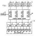
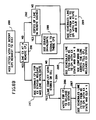
- FIG. 1 represents a multiprocessing (MP) system in which the present invention may be used.
- the MP comprises four central processors (CP's) CPO through CP3 (10, 11, 12 and 13), in which each CP includes an instruction execution (IE) unit (14, 15, 16 and 17, and a buffer control unit (BCE) 20, 21, 22 and 23, respectively.
- Each IE includes hardware and microcode that issue instructions that require the fetching and storing of operands in main storage (MS) 50.
- the IE begins a fetching or storing operation by issuing a fetch or store command to its respective cache controls (BCE) 20-23, which include a processor store-thru (ST) cache with its associated processor cache directory (PD) and all processor cache controls which are exclusively used by the associated CP (10-13).
- BCE cache controls
- the CP generally issues a fetch or store command for each doubleword (DW) unit required by an operand. If the cache line containing the DW is in the PD, which is a cache hit situation, the DW is fetched or stored in the cache in accordance with the command. For an operand fetch hit in cache, the storage access is completed without any need to go outside of the BCE. Occasionally the required DW is not in the cache, which results in a cache miss.
- DW doubleword
- the DW Before the IE fetch or store command can be completed, the DW must be fetched from the main storage. To do this, the BCE generates a corresponding fetch or store miss command which requests the storage control element (SCE) 30 to obtain from main storage 50 a line unit of data having the DW required by the IE.
- the line unit will be located in the main storage 50 on a line boundary, but the required DW will be the first DW in the fetched line to be returned to the requesting BCE (20-23) in order to keep the IE request going before the completion of the missed line transfer.
- SCE 30 connects to the CPs 10-13 and main storage 50.
- Main storage 50 is comprised of a plurality of basic storage module (BSM) controllers BSCO thru BSC3 (51, 52, 53 and 54, respectively) in which each basic storage controller (BSC) 51-54 connects to two BSMs 0(60, 62, 64 and 66) and 1 (61, 63, 65, and 67).
- BSM basic storage module
- BSC basic storage controller
- SCE 30 contains four copy directories (CDs) 31, 32, 33, and 34.
- CD contains an image of the contents of a corresponding processor cache directory (PD) in one of the BCEs in a manner similar to that described in Flusche et al, U.S. Patent No. 4,394,731. Both PD and CD are addressed by the same bit positions from the logical address.
- the CDs handle all cross-interrogate (XI) requests and can thereby better service their respective CPs.
- XI cross-interrogate
- a doubleword wide bidirectional data bus is provided between each BSM 60-67 in main storage and each SCE port, and from each SCE 30 to each CP and I/O channel controller processor 40. Along with the data busses there are also separate sets of command bus for control and address signals.
- a CP When a CP encounters cache miss for a DW access request, its BCE 20-23 initiates a line access request to main storage by sending a miss command to SCE 30, which then reissues the command to a required BSM 60-67 in main storage.
- SCE 30 In the event of a BSM busy condition, SCE 30 will save the request in a command queue and will reissue it at a later time when the required BSM 60-67 becomes available.
- SCE 30 also sequences the main storage commands in an orderly fashion so that all commands to a particular BSM are issued in first-in-first-out (FIFO) order, except when a cache conflict is found by its XI logic.
- FIFO first-in-first-out
- SCE 30 constantly monitors the status of main storage, analyzes the interrogation results of protection key and all cache directories, examines updated status of all pending commands currently being held in SCE 30, and also looks for any new BCE commands that may be waiting in BCE 20-23 to be received by SCE 30.
- SCE 30 maintains a plurality of store stacks SSO through SS3 (35-38), each for the holding of main storage store requests of up to 16 DWs for a corresponding CP.
- SCE 30 keeps enough directory information for the store stacks for the indication of main storage addresses and validity.
- SCE 30 sends a priority request to the associated BCE 20-23 to hold the sending of more store requests till the BCE 20-23 receives a later signal from SCE 30 clearing the store stack full condition.
- Data in the store stacks are updated to main storage with appropriate scheduling maintaining the incoming order within each store stack.
- a line fetch request from a CP is held by SCE 30 till the SCE makes sure that all existing stores to the line in the store stacks have been sent to the associated BSM 60-67.
- FIG. 2 shows the background organization of the instruction control at the IE unit for each CP.
- the IE at each CP has the capability of executing instructions on conditional basis. Branch prediction may be employed, although not required.
- branch prediction may be employed, although not required.
- the present description has been simplified to assume that the only cause for conditional execution is due to fetching potentially dirty data on an XIEX event, although the control of conditional execution bears much resemblance to that for branch prediction machines.
- the IE unit can reset the machine status (registers) to the point before the instruction was started.
- FIG. 3 shows the overall organization of a BCE, for example, 20.
- the BCE maintains, via BCE control 80, translation lookaside buffer (TLB) for the translation of logical main storage access addresses to real addresses, via TLB control 81.
- TLB translation lookaside buffer
- Processor Cache Directory (PD) 82 is the processor cache directory.
- Cache arrays 83 contain the actual cache data.
- the pending store stack (PSS) 84 has 8 entries. PSS 84 is used to hold DW stores from IE execution that have not yet been sent out to cache and main storage.
- the BCE control maintains a flag bit CNPHASE 85 indicating whether there is a potentially dirty cache line active at the moment.
- Figure 4 describes a typical cache control 80 within a BCE (20, for example), similar to the descriptions of U.S. Patent No. 4,484,267.
- the fetch or store request address (logical or-real) from the IE at 90 is used to select a congruence class from the processor cache directory (PD) 91.
- PD processor cache directory
- the absolute line addresses recorded at these 4 PD entries A-D are compared at 92 with the absolute request address obtained from the address translation facility 93. These addresses are compared to determine whether the line is missing in the cache or which of the 4 lines this access hits, as indicated by the SELA, SELB, SELC, and SELD signals.
- the results of the address compares are passed to both the IE unit and the array control.
- the replacement control 94 maintains the replacement status arrays, updates these status arrays when necessary, and selects the line entry to be replaced when a new line is fetched from MS.
- the PD entry write control 95 controls the update of PD entries. For a DW fetch request, in parallel to the PD read and translation processes, 4 DWs A-D in the selected congruence class are read out of the array for late select 97 when the directory address compare 92 is done. As determined by control 98, a DW data is read out at 104 to either the IE unit or the MS as needed. As described in U.S. Patent No.
- a DW store from the IE is preceded with a store interrogate (SI) request during an earlier cycle.
- SI store interrogate
- the SI request will make sure that the store can be done without a conflict such as a key violation, cache miss or absence of EX status.
- the actual DW store may be issued by the IE with direct putaway into the correct array position.
- the arrays 96 are updated under the control of 99 and 95 either by line or doubleword granularity.
- the data for array store comes at 103 from either the IE or the main storage.
- SI request should also make sure that it is possible to issue the DW store to MS or to hold it in the pending store stack (PSS). Otherwise the SI request will cause a hold of the store at the IE till the conflict gets cleared in a later cycle.
- PSS pending store stack
- FIGS. 5A and 5B provide the formats for PD (110) and CD (120) entries respectively, similar to that described in U.S. Patent 4,394,731.
- V (116,122) is the valid bit for the directory entry.
- a valid line is in exclusive (EX) state if the associated EX bit (115,121) is 1, and is in read only (RO) state otherwise.
- Each PD line entry additionally contains a protect key (PROT KEY), a line change (LC CH) bit, a fetch protect (F PROT) bit and a page change (PG CH) bit.
- PROT KEY protect key
- LC CH line change
- F PROT fetch protect
- PG CH page change
- a CD at the SCE is maintained as a mirror image for the PD at the corresponding BCE the same way as described in U.S. Patent 4,394,731.
- the contents (EX, V and ABS ADDR 117 and 123) of a CD entry should be identical to those at the corresponding PD entry except during a transition phase for a status change. Note that, since with our ST cache design all CP stores to cache will be reflected at the MS, there is no need for the LN/CH (line changed) field (113) at the PD entry which indicates whether the cache line is holding data not scheduled to be sent to MS.
- Figure 5C contains the modified format (125) for a PD entry.
- a castout for SIC design causes a changed line in a SIC to be updated at the main storage through SCE 30.
- the castout command is replaced with a DW store command, with which the BCE sends a DW store request to SCE 30 for the update of main storage upon an IE store.
- the DW data for the store will be sent down via the data bus in parallel.
- the SCE should coordinate with each BCE such that a store request from the BCE will always be received in the associated store stack (SS) at the SCE in normal conditions.
- SS store stack
- the cross-interrogate (XI) handling at the SCE by examining the CDs is similar to that in U.S. Patent 4,394,731.
- XI cross-interrogate
- a cache miss is allowed to fetch a line from main storage before the clearing procedure is complete in the XIEX situation.
- the reply signal from SCE to BCE is enhanced with an additional cleared (CLR) bit.
- CLR additional cleared
- the BCE treats this newly fetched line as potentially dirty and subject to possible abortion if used. Otherwise the fetched line is regarded valid as usual.
- the IE may issue fetch or SI request with EX intent also as described in U.S. Patent 4,394,731. Such a request can be successfully handled only when the requested DW hits to a cache line with EX bit on. A fetch request with RO intent only requires the line valid in the cache with V bit on. Protection errors and other exceptions in cache access will be handled by special exception logic.
- PSS 132 is implemented as a circular FIFO queue with 8 entries, labelled 0 through 7. Each PSS entry contains DW data for a store issued from IE.
- FIG. 6B shows the format of a PSS directory entry 140, including their sizes in bits.
- At each PSS directory entry there are at least three fields: absolute DW address field STRADDR (28 bits) 144, two flag bits CRLSE (1 bit) 141 and MSONLY (1 bit) 142, and a field STRCOORD 143 recording the cache position for the stored DW.
- CRLSE 141 bit is on the DW store is under conditional phase and cannot be released to main storage.
- each BCE is required to not allow more than one outstanding request to be issued to the SCE at any moment, except store releases from PSS to the main storage for finished or unconditionally executed instructions.
- store releases from PSS to the main storage for finished or unconditionally executed instructions The following descriptions will also ignore handling for exception conditions.
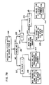
- FIG. 7A is a flowchart showing BCE handling upon receiving a fetch request (200) with RO intent from the IE unit.
- the IE idles and waits for the missed DW to arrive from MS.
- the DW is accessed from cache without delay if it does not conflict with any of the possibly existing DW stores in the PSS (step 205).
- Figure 7B contains a flowchart for BCE handling upon receiving a fetch request with EX intent from the IE unit (step 210).
- the fetch is carried out (step 213) without delay if the line is resident in cache (step 211) with EX state (step 212).
- the BCE issues a request for EX status to the SCE (step 215) when possible.
- the line misses in cache step 211) the BCE issues a miss fetch request with EX intent to the SCE (step 218) when possible.
- Such SCE requests are held if conditional execution is in effect (steps 216 and 219).
- FIG. 7C contains a flowchart for BCE handling upon receiving a store interrogate (SI) request with EX intent from the IE unit (step 220).
- SI store interrogate
- the operation of BCE is similar to those described in Figure 7B, except that no DW fetch to IE is needed.
- the BCE records the cache coordinate found for the DW in anticipation of oncoming store from IE.
- the fetch is carried out (step 226) without delay if the line is resident in cache (step 221) with EX state (step 222). If the DW hits to a RO line in cache (step 223) the BCE issues a request for EX status to the SCE (step 224) when possible. If the line misses in cache (step 221) the BCE issues a miss fetch request with EX intent to the SCE (step 228) when possible.
- Such SCE requests are held if conditional execution is in effect (steps 225 and 229).
- Figure 7D contains a flowchart for BCE handling upon receiving a store request from the IE unit (step 230).
- the DW store is put on PSS if possible (steps 232 and 233).
- PSS is full (step 234) the store will be held till PSS has room available.
- the MSONLY flag is set to 0 at the associated PSS entry in order to necessitate the cache store put away when the store is released later on (step 233).
- the SCE When the SCE receives a DW store request from CPi the request is simply queued onto the store stack SSi at the SCE. The SCE will constantly update DW stores from the store stacks to main storage when possible.
- the SCE may receive three major requests from a BCE.
- a miss fetch with RO intent requests a cache line transfer from main storage with RO state.
- a miss fetch with EX intent requests a line transfer from main storage with EX status.
- the third request type is Upgrade to EX status which requests only the Ex status for a cache line that is already resident at the BCE with RO state.
- a request from BCE may trigger cross-interrogate (XI) actions.
- XI cross-interrogate
- the SCE handles XIs in a manner similar to but differently from the scheme described in U.S. Patent No. 4,394,731. The maintenance of CDs and the searching of them in determining XI condition are similar, but different algorithms are used in resolving XIs.
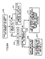
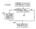
- FIGs. 8A-C are flowcharts describing the SCE handling for the three requests from BCEs.
- FIG. 8A contains the flowchart for SCE handling of a line miss request from CPi with RO intent (step 270). If the line is not held EX remotely (271), the SCE schedules a line fetch from main storage to CPi and signals CPi with a receive line signal with CLR bit on (step 272). Now assume that CPj ( j ⁇ i) is holding the line EX. The SCE sends out change EX to RO (CERO) signal to CPj (step 273). Then the SCE checks whether the line overlaps with any outstanding DW in the store stack SSj (step 274).
- the SCE does not schedule a main storage line fetch (step 277) until conflicting stores in store stacks are cleared.
- the reason for not scheduling conditional main storage line fetch when the SCE detects outstanding store conflicts is that CPj is more likely to generate more stores in this case.
- FIG. 8B shows the SCE operations for a line fetch request with EX intent from CPi (step 280). It is similar to the procedures described in FIG. 8A, except that the SCE needs to send invalidate line signal to all CPs that holds a copy of the line as indicated in the CDs.
- the SCE schedules a line fetch from main storage to CPi and signals CPi with a receive line signal with CLR bit on (step 289). If CPj (j ⁇ i) is holding the line EX, the SCE signals CPj to invalidate the line (step 283). Then the SCE checks whether the line overlaps with any outstanding DW in the store stack SSj (step 284).
- the SCE does not schedule a main storage line fetch (step 287) until conflicting stores in store stacks are cleared.
- the reason for not scheduling conditional main storage line fetch when the SCE detects outstanding store conflicts is that CPj is more likely to generate more stores in this case.
- FIG. 8C describes the SCE operations for an upgrade to EX request from from CPi (step 290).
- the line is already valid and RO at the BCE of CPi. If it determines that the line is held in remote caches (step 291) the SCE only needs to send out invalidate signals to those BCEs that contain copies of the line (step 292).
- the design should make sure that all the invalidate signal recipients get the signals not after CPi receives the signal for upgrading RO state to EX (step 293).
- the timing control depends on the specific implementation environment.
- a conditional line fetch from main storage to CPi may be scheduled before the SCE finalizes the release of EX state of the line held by CPj ( j ⁇ i ). It is possible that the SCE receives from CPj subsequent stores on the line before an acknowledgement on the release of EX status. In this situation the SCE should notify CPi to abort the conditionally fetched data through a regular line invalidate signal. On the other hand, if the SCE receives from CPj the acknowledgement of releasing EX state without generating extra stores to the line, the SCE may then finalize the state change and sends a confirm status signal to CPi. After CPi receives the confirm status signal, the BCE will discard the conditional status of the line as will be described later.
- the SCE will not finalize the release of EX state of a line by a CP until it is sure that the relevant stores in the associated store stack SS are cleared into main storage. This is not a necessary requirement in general. The assumption is made in this description in order to simplify the description of the design. Also it is assumed that the SCE serializes the handling of XIs properly. The SCE will not issue an XI request on a line to a CP before the SCE has completed the handling of an earlier request from the CP itself.
- the BCE of a CP may receive the following four major signals from the SCE: receive line, confirm status, CERO, and line invalidate.
- FIGs. 9A-D are flowcharts for the BCE actions upon receiving these signals.
- FIG. 9A shows the BCE action for a receive line signal from SCE (step 300).
- the BCE gets ready to receive data from main storage later on (step 301). If the CLR bit is 1 in the signal (step 302), indicating an unconditional fetch, the BCE waits for the arrival for data as usual (step 304). If the CLR bit is 0 (step 302), indicating a conditional transfer, the BCE will start the conditional execution phase as described with respect to FIG. 10 (step 303).
- FIG. 9B describes the BCE actions upon receiving a confirm status signal from the SCE (step 310). In this situation there should already be a conditionally fetched line outstanding.
- the BCE resets the conditional execution phase by turning off its CNPHASE flag and by resetting all the CRLSE bits to 0 in the PSS directory.
- the BCE also signals the IE unit to reset its CNFLG register to 0 (step 311).
- FIG. 9C describes the BCE actions upon receiving a CERO request from the SCE (step 320).
- FIG. 9D shows the BCE actions upon receiving a line invalidate request from the SCE (330). The operation is similar to that for the handling of a CERO request.
- FIG. 10 describes the actions of BCE and IE for starting the conditional execution phase.
- the BCE receives a line fetch signal with CLR bit on from the SCE (step 340)
- the BCE sets CNPHASE to 1 and assigns the value of the NXTSTR index register to the CNSTR register for PSS management.
- the BCE also signals the IE unit to start conditional execution (step 341).
- the CNFLG is first turned on the IE unit records the instruction address in the register CNIADDR (step 342).
- any store queued on PSS will cause the CRLSE and MSONLY bits turned off, the NXTSTR register incremented by 1 (modulo 8), and PSSFREE decremented by 1. Also, the position of the cache line, as identified by the preceding SI command, will be recorded at the STRCOORD field at the new PSS entry.
- a store may also be pushed on PSS when the store stack at the SCE is full, although the DW is putaway into the cache. In this situation, at the PSS entry, the MSONLY bit is turned on and the CRLSE bit is also on.
- FIG. 11 describes BCE operations at CPi for locating the next store to release from PSS.
- the BCE constantly examines the PSS for next pending store to release to SCE.
- the next store in PSS is indexed by the NXTRLSE register (step 350).
- the next store on PSS cannot be released if NXTRLSE is equal to NXTSTR (indicating empty PSS) or if the CRLSE bit is on (indicating conditional store) (step 351).
- NXTRLSE indicating empty PSS
- CRLSE bit indicating conditional store
- the BCE increments the register NXTRLSE by 1 (modulo 8) (step 357) and increments PSSFREE by 1.
- the released PSS store entry has the MSONLY bit off (step 355) the DW is also putaway into the cache positioned by the STRCOORD field at the PSS directory entry (step 356).
- the BCE resets the CNPHASE flag to 0 and clears all the conditional stores at the PSS by resetting NXTSTR register with the value of CNSTR register and by adjusting PSSFREE.
- the IE unit When the IE unit is signaled for abortion, it turns the CNFLG off and restarts the execution of the instruction recorded by the CNIIDX address register.
- Restarting execution involves resetting machine state properly, according to the particular implementation.
- One simple technique is for the IE to copy the machine state like PSW and GPRs before the conditional execution.
Landscapes
- Engineering & Computer Science (AREA)
- Theoretical Computer Science (AREA)
- Physics & Mathematics (AREA)
- General Engineering & Computer Science (AREA)
- General Physics & Mathematics (AREA)
- Memory System Of A Hierarchy Structure (AREA)
- Advance Control (AREA)
- Multi Processors (AREA)
Claims (4)
- Verfahren, das auf ein Mehrprozessor-Computersystem anwendbar ist, das eine Vielzahl von Prozessoren (10, 11, 12, 13) enthält sowieeinen lokalen Cache (20, 21, 22, 23) für jeden der Rechner (10, 11, 12, 13),einen Hauptspeicher (50), der unter den Rechnern (10, 11, 12, 13) anteilig genutzt wird, mit Leitungen, die es den Rechnern (10, 11, 12, 13) erlauben, in diesem Hauptspeicher (50) zu operieren,wobei das Verfahren ein übereinstimmendes Steuerschema enthält, um wenigstens zwei alternative Status der Leitungen anzugeben:- der erste alternative Status erlaubt irgendeinem Rechner (10, 11, 12, 13) aus der Leitung zu lesen, jedoch nicht in die Leitung zu schreiben,- der zweite alternative Status für eine Leitung wird durch einen besonderen Rechner (10, 11, 12, 13) gehalten, um aus dieser Leitung zu lesen und in diese zu schreiben,wobei sich das Verfahren außerdem auf das Abrufen einer Leitung aus dem Hauptspeicher (50) in den lokalen Cache eines ersten Rechners (10, 11, 12, 13) bezieht, wenn ein zweiter Rechner (10, 11, 12, 13) diese Leitung in dem zweiten Status hält, wobei der erste Schritt des Verfahrensverlangt, daß der Status dieser Leitung in einen Status geändert wird, der es dem ersten Rechner ( 10, 11, 12, 13) erlaubt, aus dieser Leitung auszulesen und wobei das Verfahren durch die weiteren Schritte gekennzeichnet ist:vorläufiger Abruf dieser Leitung in den lokalen Cache des ersten Rechners (10, 11, 12, 13), ohne auf die angeforderte Änderung im Status dieser Leitung zu warten, indem diese Leitung immer noch im zweiten Status für den zweiten Rechner (10, 11, 12, 13) gehalten wird, wobei der vorläufige Abruf durch den ersten Rechner (10, 11, 12, 13) den Zugriff auf diese Leitung erlaubt, indem dem ersten Rechner (10, 11, 12, 13) nach Durchführung der angeforderten Änderung im Status bestätigt wird, ob diese Leitung geändert wurde, nachdem diese vorläufig abgerufen wurde und indem alle Rechneraktivitäten, die aus dem Zugriff resultieren, bedingt zurückgesetzt werden, wenn die Bestätigung bezüglich der Änderung des Leitungsstatus negativ ist.
- Verfahren gemäß Anspruch 1, das durch die folgenden Schritte gekennzeichnet wird:Betrieb mittels Befehlen, die von diesem Leitungsabruf abhängig sind undbedingter Abbruch aller Operationen, die von der Gültigkeit dieser Leitung abhängig sind und erneutes Starten dieser Operationen, wenn die Bestätigung zu der Änderung von dieser Leitung negativ ist.
- Verfahren gemäß Anspruch 1 oder 2, das dadurch gekennzeichnet wird, daß
der Status der Leitung, der geändert wird wie dies von dem ersten Verfahrensschritt verlangt wurde, der erste alternative Status ist. - Verfahren gemäß Anspruch 1 oder 2, das dadurch gekennzeichnet wird,
daß der Status der Leitung, der geändert wird wie dies von dem ersten Verfahrensschritt verlangt wurde, der zweite alternative Status für den ersten Rechner anstelle für den zweiten Rechner ist.
Applications Claiming Priority (2)
| Application Number | Priority Date | Filing Date | Title |
|---|---|---|---|
| US280034 | 1981-07-02 | ||
| US07/280,034 US5018063A (en) | 1988-12-05 | 1988-12-05 | Method for reducing cross-interrogate delays in a multiprocessor system |
Publications (3)
| Publication Number | Publication Date |
|---|---|
| EP0372201A2 EP0372201A2 (de) | 1990-06-13 |
| EP0372201A3 EP0372201A3 (de) | 1991-09-04 |
| EP0372201B1 true EP0372201B1 (de) | 1996-01-17 |
Family
ID=23071356
Family Applications (1)
| Application Number | Title | Priority Date | Filing Date |
|---|---|---|---|
| EP89119148A Expired - Lifetime EP0372201B1 (de) | 1988-12-05 | 1989-10-16 | Verfahren zum Abrufen von potentiell ungültigen Daten in einem Mehrrechnersystem |
Country Status (4)
| Country | Link |
|---|---|
| US (1) | US5018063A (de) |
| EP (1) | EP0372201B1 (de) |
| JP (1) | JPH0670779B2 (de) |
| DE (1) | DE68925470T2 (de) |
Families Citing this family (24)
| Publication number | Priority date | Publication date | Assignee | Title |
|---|---|---|---|---|
| US5185875A (en) * | 1989-01-27 | 1993-02-09 | Digital Equipment Corporation | Method and apparatus for reducing memory read latency in a shared memory system with multiple processors |
| US5226126A (en) * | 1989-02-24 | 1993-07-06 | Nexgen Microsystems | Processor having plurality of functional units for orderly retiring outstanding operations based upon its associated tags |
| US5781753A (en) * | 1989-02-24 | 1998-07-14 | Advanced Micro Devices, Inc. | Semi-autonomous RISC pipelines for overlapped execution of RISC-like instructions within the multiple superscalar execution units of a processor having distributed pipeline control for speculative and out-of-order execution of complex instructions |
| US5768575A (en) * | 1989-02-24 | 1998-06-16 | Advanced Micro Devices, Inc. | Semi-Autonomous RISC pipelines for overlapped execution of RISC-like instructions within the multiple superscalar execution units of a processor having distributed pipeline control for sepculative and out-of-order execution of complex instructions |
| US5214766A (en) * | 1989-04-28 | 1993-05-25 | International Business Machines Corporation | Data prefetching based on store information in multi-processor caches |
| JPH04246745A (ja) * | 1991-02-01 | 1992-09-02 | Canon Inc | 情報処理装置及びその方法 |
| DE69323790T2 (de) * | 1992-04-29 | 1999-10-07 | Sun Microsystems Inc | Verfahren und Vorrichtung für mehreren ausstehende Operationen in einem cachespeicherkohärenten Multiprozessorsystem |
| JP2788836B2 (ja) * | 1992-05-15 | 1998-08-20 | インターナショナル・ビジネス・マシーンズ・コーポレイション | ディジタルコンピュータシステム |
| JPH06282528A (ja) * | 1993-01-29 | 1994-10-07 | Internatl Business Mach Corp <Ibm> | データ転送方法及びそのシステム |
| JPH0793216A (ja) * | 1993-09-27 | 1995-04-07 | Hitachi Ltd | キャッシュ記憶制御装置 |
| US5590309A (en) * | 1994-04-01 | 1996-12-31 | International Business Machines Corporation | Storage protection cache and backing storage having system control element data cache pipeline and storage protection bits in a stack array with a stack directory for the stack array |
| JP2641396B2 (ja) * | 1994-08-30 | 1997-08-13 | 甲府日本電気株式会社 | ページ履歴メモリ装置 |
| JPH0950400A (ja) * | 1995-08-10 | 1997-02-18 | Nec Corp | マルチプロセッサシステム |
| US5881303A (en) * | 1996-07-01 | 1999-03-09 | Sun Microsystems, Inc. | Multiprocessing system configured to perform prefetch coherency activity with separate reissue queue for each processing subnode |
| US5900015A (en) * | 1996-08-09 | 1999-05-04 | International Business Machines Corporation | System and method for maintaining cache coherency using path directories |
| US5991825A (en) * | 1997-07-11 | 1999-11-23 | International Business Machines Corporation | System for handling missed revolution in a disk drive by aborting the execution of primary command and executing secondary command if a missed revolution occurs |
| US6098115A (en) * | 1998-04-08 | 2000-08-01 | International Business Machines Corporation | System for reducing storage access latency with accessing main storage and data bus simultaneously |
| US6112283A (en) * | 1998-08-06 | 2000-08-29 | Intel Corporation | Out-of-order snooping for multiprocessor computer systems |
| US20070260754A1 (en) * | 2006-04-13 | 2007-11-08 | Irish John D | Hardware Assisted Exception for Software Miss Handling of an I/O Address Translation Cache Miss |
| US8544687B2 (en) * | 2007-08-31 | 2013-10-01 | Momentive Performance Materials, Inc. | Display card with viscous material dispenser |
| US10402324B2 (en) * | 2013-10-31 | 2019-09-03 | Hewlett Packard Enterprise Development Lp | Memory access for busy memory by receiving data from cache during said busy period and verifying said data utilizing cache hit bit or cache miss bit |
| US10943294B1 (en) | 2017-05-10 | 2021-03-09 | State Farm Mutual Automobile Insurance Company | Continuously monitoring and updating mortgage ready data |
| US10949919B1 (en) | 2017-05-10 | 2021-03-16 | State Farm Mutual Automobile Insurance Company | Approving and updating dynamic mortgage applications |
| US11094007B1 (en) | 2017-05-10 | 2021-08-17 | State Farm Mutual Automobile Insurance Company | Continuously updating mortgage ready data |
Family Cites Families (18)
| Publication number | Priority date | Publication date | Assignee | Title |
|---|---|---|---|---|
| US4208716A (en) * | 1978-12-11 | 1980-06-17 | Honeywell Information Systems Inc. | Cache arrangement for performing simultaneous read/write operations |
| US4471429A (en) * | 1979-12-14 | 1984-09-11 | Honeywell Information Systems, Inc. | Apparatus for cache clearing |
| US4345309A (en) * | 1980-01-28 | 1982-08-17 | Digital Equipment Corporation | Relating to cached multiprocessor system with pipeline timing |
| US4349871A (en) * | 1980-01-28 | 1982-09-14 | Digital Equipment Corporation | Duplicate tag store for cached multiprocessor system |
| JPS601656B2 (ja) * | 1980-05-14 | 1985-01-16 | 日本電気株式会社 | 緩衝記憶回路 |
| US4394731A (en) * | 1980-11-10 | 1983-07-19 | International Business Machines Corporation | Cache storage line shareability control for a multiprocessor system |
| US4481573A (en) * | 1980-11-17 | 1984-11-06 | Hitachi, Ltd. | Shared virtual address translation unit for a multiprocessor system |
| US4414624A (en) * | 1980-11-19 | 1983-11-08 | The United States Of America As Represented By The Secretary Of The Navy | Multiple-microcomputer processing |
| US4439829A (en) * | 1981-01-07 | 1984-03-27 | Wang Laboratories, Inc. | Data processing machine with improved cache memory management |
| JPS58154044A (ja) * | 1982-03-05 | 1983-09-13 | Nec Corp | 情報処理装置 |
| US4503497A (en) * | 1982-05-27 | 1985-03-05 | International Business Machines Corporation | System for independent cache-to-cache transfer |
| US4686621A (en) * | 1983-06-30 | 1987-08-11 | Honeywell Information Systems Inc. | Test apparatus for testing a multilevel cache system with graceful degradation capability |
| US4875155A (en) * | 1985-06-28 | 1989-10-17 | International Business Machines Corporation | Peripheral subsystem having read/write cache with record access |
| US4727486A (en) * | 1986-05-02 | 1988-02-23 | Honeywell Information Systems Inc. | Hardware demand fetch cycle system interface |
| EP0498472B1 (de) * | 1986-08-12 | 1994-10-12 | Hitachi, Ltd. | Mikroprozessor zur Datentransferwiederholung |
| US4833601A (en) * | 1987-05-28 | 1989-05-23 | Bull Hn Information Systems Inc. | Cache resiliency in processing a variety of address faults |
| JPH0195344A (ja) * | 1987-10-07 | 1989-04-13 | Matsushita Electric Ind Co Ltd | キャッシュ・メモリー |
| US4831622A (en) * | 1987-12-22 | 1989-05-16 | Honeywell Bull Inc. | Apparatus for forcing a reload from main memory upon cache memory error |
-
1988
- 1988-12-05 US US07/280,034 patent/US5018063A/en not_active Expired - Fee Related
-
1989
- 1989-09-20 JP JP1242402A patent/JPH0670779B2/ja not_active Expired - Lifetime
- 1989-10-16 DE DE68925470T patent/DE68925470T2/de not_active Expired - Fee Related
- 1989-10-16 EP EP89119148A patent/EP0372201B1/de not_active Expired - Lifetime
Also Published As
| Publication number | Publication date |
|---|---|
| EP0372201A2 (de) | 1990-06-13 |
| JPH0670779B2 (ja) | 1994-09-07 |
| EP0372201A3 (de) | 1991-09-04 |
| JPH02166539A (ja) | 1990-06-27 |
| DE68925470D1 (de) | 1996-02-29 |
| US5018063A (en) | 1991-05-21 |
| DE68925470T2 (de) | 1996-08-14 |
Similar Documents
| Publication | Publication Date | Title |
|---|---|---|
| EP0372201B1 (de) | Verfahren zum Abrufen von potentiell ungültigen Daten in einem Mehrrechnersystem | |
| US5490261A (en) | Interlock for controlling processor ownership of pipelined data for a store in cache | |
| US5148533A (en) | Apparatus and method for data group coherency in a tightly coupled data processing system with plural execution and data cache units | |
| JP3927556B2 (ja) | マルチプロセッサ・データ処理システム、変換索引バッファ無効化インストラクション(tlbi)のハンドリングを行うための方法、およびプロセッサ | |
| US6704841B2 (en) | Method and apparatus for facilitating speculative stores in a multiprocessor system | |
| EP1399823B1 (de) | Verfahren zur verwendung eines l2-verzeichnisses, um spekulatives laden in einem mehrprozessorsystem zu ermöglichen | |
| EP0514024B1 (de) | Verfahren und Vorrichtung für eine verbesserte Speicherarchitektur | |
| US5230070A (en) | Access authorization table for multi-processor caches | |
| EP0450285A2 (de) | Cache-Speicher | |
| EP0436092A2 (de) | Datenverarbeitungssystem mit ausserhalb der Folge Ablaufabrufsteuerungen | |
| US6374332B1 (en) | Cache control system for performing multiple outstanding ownership requests | |
| US20080140935A1 (en) | Efficient marking of shared cache lines | |
| US20020199066A1 (en) | Method and apparatus for facilitating speculative loads in a multiprocessor system | |
| US10140052B2 (en) | Memory access in a data processing system utilizing copy and paste instructions | |
| US20090106498A1 (en) | Coherent dram prefetcher | |
| WO2002054250A2 (en) | Method and apparatus for controlling memory storage locks based on cache line ownership | |
| US5214766A (en) | Data prefetching based on store information in multi-processor caches | |
| US5016168A (en) | Method for storing into non-exclusive cache lines in multiprocessor systems | |
| EP0380842A2 (de) | Verfahren und Vorrichtung zur Schnittstellenbildung zwischen einer Systemsteuereinheit für ein Multiprozessorsystem und den zentralen Verarbeitungseinheiten | |
| US6973541B1 (en) | System and method for initializing memory within a data processing system | |
| US7065614B1 (en) | System and method for maintaining memory coherency within a multi-processor data processing system | |
| US6460100B1 (en) | Bus snooper for SMP execution of global operations utilizing a single token with implied release | |
| US7774552B1 (en) | Preventing store starvation in a system that supports marked coherence | |
| AU628531B2 (en) | Method and apparatus for interfacing a system control unit for a multiprocessor system with the central processing units | |
| EP0394642A2 (de) | Datenvorausholung in Cachespeichern |
Legal Events
| Date | Code | Title | Description |
|---|---|---|---|
| PUAI | Public reference made under article 153(3) epc to a published international application that has entered the european phase |
Free format text: ORIGINAL CODE: 0009012 |
|
| AK | Designated contracting states |
Kind code of ref document: A2 Designated state(s): DE FR GB |
|
| 17P | Request for examination filed |
Effective date: 19901025 |
|
| PUAL | Search report despatched |
Free format text: ORIGINAL CODE: 0009013 |
|
| AK | Designated contracting states |
Kind code of ref document: A3 Designated state(s): DE FR GB |
|
| 17Q | First examination report despatched |
Effective date: 19940504 |
|
| GRAA | (expected) grant |
Free format text: ORIGINAL CODE: 0009210 |
|
| AK | Designated contracting states |
Kind code of ref document: B1 Designated state(s): DE FR GB |
|
| REF | Corresponds to: |
Ref document number: 68925470 Country of ref document: DE Date of ref document: 19960229 |
|
| ET | Fr: translation filed | ||
| PGFP | Annual fee paid to national office [announced via postgrant information from national office to epo] |
Ref country code: FR Payment date: 19961007 Year of fee payment: 8 |
|
| PGFP | Annual fee paid to national office [announced via postgrant information from national office to epo] |
Ref country code: DE Payment date: 19961030 Year of fee payment: 8 |
|
| PLBE | No opposition filed within time limit |
Free format text: ORIGINAL CODE: 0009261 |
|
| STAA | Information on the status of an ep patent application or granted ep patent |
Free format text: STATUS: NO OPPOSITION FILED WITHIN TIME LIMIT |
|
| 26N | No opposition filed | ||
| PGFP | Annual fee paid to national office [announced via postgrant information from national office to epo] |
Ref country code: GB Payment date: 19970923 Year of fee payment: 9 |
|
| PG25 | Lapsed in a contracting state [announced via postgrant information from national office to epo] |
Ref country code: FR Free format text: THE PATENT HAS BEEN ANNULLED BY A DECISION OF A NATIONAL AUTHORITY Effective date: 19971031 |
|
| PG25 | Lapsed in a contracting state [announced via postgrant information from national office to epo] |
Ref country code: DE Free format text: LAPSE BECAUSE OF NON-PAYMENT OF DUE FEES Effective date: 19980701 |
|
| REG | Reference to a national code |
Ref country code: FR Ref legal event code: ST |
|
| PG25 | Lapsed in a contracting state [announced via postgrant information from national office to epo] |
Ref country code: GB Free format text: LAPSE BECAUSE OF NON-PAYMENT OF DUE FEES Effective date: 19981016 |
|
| GBPC | Gb: european patent ceased through non-payment of renewal fee |
Effective date: 19981016 |