EP0366831B1 - Temperaturkompensationsschaltung - Google Patents
Temperaturkompensationsschaltung Download PDFInfo
- Publication number
- EP0366831B1 EP0366831B1 EP88118442A EP88118442A EP0366831B1 EP 0366831 B1 EP0366831 B1 EP 0366831B1 EP 88118442 A EP88118442 A EP 88118442A EP 88118442 A EP88118442 A EP 88118442A EP 0366831 B1 EP0366831 B1 EP 0366831B1
- Authority
- EP
- European Patent Office
- Prior art keywords
- temperature
- voltage
- pulse width
- resistor
- temperature compensating
- Prior art date
- Legal status (The legal status is an assumption and is not a legal conclusion. Google has not performed a legal analysis and makes no representation as to the accuracy of the status listed.)
- Expired - Lifetime
Links
Images


Classifications
-
- G—PHYSICS
- G01—MEASURING; TESTING
- G01R—MEASURING ELECTRIC VARIABLES; MEASURING MAGNETIC VARIABLES
- G01R19/00—Arrangements for measuring currents or voltages or for indicating presence or sign thereof
- G01R19/32—Compensating for temperature change
-
- G—PHYSICS
- G01—MEASURING; TESTING
- G01D—MEASURING NOT SPECIALLY ADAPTED FOR A SPECIFIC VARIABLE; ARRANGEMENTS FOR MEASURING TWO OR MORE VARIABLES NOT COVERED IN A SINGLE OTHER SUBCLASS; TARIFF METERING APPARATUS; MEASURING OR TESTING NOT OTHERWISE PROVIDED FOR
- G01D3/00—Indicating or recording apparatus with provision for the special purposes referred to in the subgroups
- G01D3/028—Indicating or recording apparatus with provision for the special purposes referred to in the subgroups mitigating undesired influences, e.g. temperature, pressure
- G01D3/036—Indicating or recording apparatus with provision for the special purposes referred to in the subgroups mitigating undesired influences, e.g. temperature, pressure on measuring arrangements themselves
- G01D3/0365—Indicating or recording apparatus with provision for the special purposes referred to in the subgroups mitigating undesired influences, e.g. temperature, pressure on measuring arrangements themselves the undesired influence being measured using a separate sensor, which produces an influence related signal
Definitions
- the present invention relates to a temperature compensating circuit for subjecting a detected signal (measured signal voltage) by various kinds of analyzers, such as a gas analyzer, to a temperature compensating treatment.
- a known oxygen meter is adapted to have a plurality of displaying functions, such as the display of dissolved oxygen in a partial pressure ratio and the display of a dissolved oxygen (DO) in a concentration, in addition to the display of the detected temperature itself. It is, however, necessary to subject the measured signal to individual temperature compensating treatments for the respective displays. Some other gas analyzers are able to analyze concentrations of a plurality of kinds of gases also. In such cases it its also necessary to subject the detected signals of concentrations of the respective gases to the individual temperature compensating treatment.
- the conventional temperature compensating circuit is adapted to provide a temperature sensitive (resistance) element r T in a feedback circuit portion of an operational amplifier a, in which a measured signal voltage V is fed, or in an input circuit portion of said operational amplifier a (any one of them is selected depending upon the polarity of the temperature characteristics of the measured signal voltage) to change the gain of the operational amplifier a in response to the temperature.
- the result is a temperature compensated measured signal voltageV0.
- a temperature compensating circuit capable of carrying out the compensation for a plurality of measured signal voltages, respectively, by means of only one temperature sensitive element and by using a detected temperature signal obtained by said one temperature sensitive element.
- This temperature compensating circuit has been proposed in Japanese Patent Application No. Sho 57-44869 (Japanese Patent Laid-Open No. Sho 58-160859), Japanese Utility Model Application No. Sho 60-146072 (Japanese Utility Model Laid-Open No. Sho 62-53356) and the like.
- this improved temperature compensating circuit still has the following problems: In the case where the temperature compensating circuit is constructed for carrying out the temperature compensation for a plurality of measured signal voltages, respectively, and because only one temperature sensitive (resistance) element is sufficient but one comparatively expensive operational amplifier is necessary for a plurality of measured signal voltages, respectively, not only the reduction of the costs of the production and the simplification and miniaturization in construction are not sufficiently realized but also the disadvantages (ii), (iii) incidental to the temperature compensating circuit having the above described conventional construction are still not eliminated.
- thermoelectric circuit capable of remarkably reducing the number of constituent part, simplifying and miniaturizing inexpensively the construction, remarkably lowering the difficulties for the design corresponding to the temperature characteristics of the measured signal voltage and carrying out a temperature compensation with a remarkably higher accuracy.
- the present invention provides a temperature compensating circuit comprising:
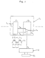
- X designateds one temperature-pulse width conversion circuit portion adapted to generate the pulse width signal V p (this will be mentioned in detail) of the duty ratio D(T) in response to the temperature detected by the temperature sensitive element R T , Y1,..., Y N designate temperature compensating circuit portions connected to said temperature-pulse width conversion circuit protion X and adapted to apply the temperature compensating treatment to the measured signal voltage V NI derived from the input terminal I N and then to give out the measured signal voltage V ND which has been compensated through the output terminal O N , respectively.
- Said temperature-pulse width conversion circuit portion X comprises a temperature measuring portion 1 producing a voltage V T corresponding to the temperature and a voltage-pulse width converter 2 putting out the pulse width signal V p .
- Said temperature measuring circuit portion 1 comprises a feedback resistor R B , the temperature sensitive (resistance) element R T , such as a thermistor, a resistor R C for improving the linearity and the like. Said resistors are provided in the feedback circuit portion of the operational amplifier A.
- the non-inverting input terminal of this operational amplifier A is grounded and its inverting input terminal is connected to a reference power source E and an input resistor R A .
- the voltage-pulse width converter 2 has the known construction comprising a triangular wave generator 3 and a comparator 4 to which a triangular wave-shaped pulse from the triangular wave generator 3 and the voltage V T from said temperature measuring circuit portion 1 are supplied.
- the temperature compensating circuit portion Y N (all temperature compensating circuit portions have the same construction, so that here merely the N-th temperature compensating circuit portion Y N is described) comprises a first resistor R 1N , a second resistor R 2N and a third resistor R 3N connected in series so that the measured signal voltage V N1 derived from the input terminal I N may be divided into the large signal voltage V NB and the small signal voltage V ND (V NB > V NS ) and given out.
- This temperature compensating circuit portion Y N is provided with the voltage-dividing means C N comprising a signal output line 5 and a signal output line 6 extending from between the first resistor R 1N and the second resistor R 2N and between the second resistor R 2N and the third resistor R 3N , respectively.
- the changeover means D N is comprising a switching element, such as an analog switch, so that the large and small signal voltages V NB , V NS are supplied through the signal output lines 5 and 6 from the voltage-dividing means C N and can alternately fed to said output terminal O N in response to the HIGH/LOW change of the pulse width signal V p .
- the pulse width signal V p is supplied from said temperature-pulse width conversion circuit portionX.
- the weighted average value of said large and small signal voltages V NB , V NS which are changed in response to the duty ratio D(T) of the pulse width signal V p is supplied to said output terminal O N as the measured signal voltage V NO which has been subjected to the temperature compensation.
- the change-over characteristics of said change-over means D N may be suitably determined depending upon the polarity of the measured signal voltage V NI . But in the case where the change-over means D N with the same change-over characteristics is used independent of the polarity of the measured signal voltage V NI , an inverting element N may be provided in the signal line extending from the temperature-pulse width conversion circuit portion X to the change-over means D N if necessary.
- said change-over means D N is set so that the large signal voltage V NB is connected to the output terminal O N when the pulse width signal V p is HIGH. While the small signal voltage V NS is connected to the output terminal O N when the pulse width signal V p is LOW.
- the weighted average value V NO of said large and small signal voltages V NB , V NS supplied to the output terminal O N is expressed by the following equation 1:
- a temperature coefficient V N0 /V NI of the temperature compensating circuit portion Y N is dependent upon said duty ratio D(T) of the pulse width signal V p (in short, the temperature characteristics of the temperature-pulse width conversion circuit portion X), upon R 3N /(R 1N + R 2N + R 3N ) and upon R 2N /R 3N .
- the temperature coefficient V N0 /V NI of the temperature compensating circuit portion Y N depends on said duty ratio D(T) of the pulse width signal V p , on (R 2N + R 3N )/(R 1N + R 2N + R 3N ) and on R 2N /(R 2N + R 3N ).
- the resistance value of said first resistor R 1N is equal to that of said third resistor R 3N and said second resistor R 2N is a variable resistor and furthermore said temperature-pulse width conversion circuit portion X is set so that the duty ratio D (T) of the pulse width signal V p given out therefrom may amount to 0.5 when the temperature T is equal to the reference temperature T0 (for example 20°C), as shown in Fig.
- variable resistor the second resistor R 2N
- the output V N0 of the temperature compensating circuit portion Y N at a temperature T (for example 40°C) different from the reference temperature T0 may have the same value as that at said reference temperature T0.
- said first resistor R 1N may be omitted. It is rather desirable to omit the first resistor R 1N from a viewpoint of still more simplifying the design calculations for determining the needed resistance value.
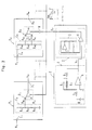
- Fig. 4(A), (B) show the modifications of said temperature-pulse width conversion circuit portion X.
- the temperature-pulse width conversion circuit portion X is having the so-called open loop construction, in which the voltage V T corresponding to the temperature is generated by means of the temperature measuring circuit portion 1.
- the generated voltage V T is supplied to the voltage-pulse width converter 2 to obtain the pulse width signal V p having the duty ratio D(T) corresponding to the temperature T, as shown.
- the temperature-pulse width conversion circuit portion X according to these modifications has the following closed loop construction.
- the temperature-pulse width conversion circuit portion X shown in Fig. 4(A) comprises an integration circuit dividing a first reference voltage V1 by means of a first resistor R i and a second resistor R ii .
- the divided voltages are supplied in a non-inverting input terminal of an operational amplifier A and through a third resistor R iii to its inverting input terminal.
- the output from the operational amplifier A is fed back to its inverting input terminal through a capacitor C.
- This circuit is further provided with a voltage-pulse width converter 2 having the same construction as the above described one and forming a pulse width signal V p having a duty ratio D(T) corresponding to an output voltage V from the integration circuit and with a switch-over means S.
- This switch-over means S is a switching element, such as an analog switch, carrying out the switch-over operation by the pulse width signal V p .
- One of said first to fourth resistors R i to R iv is formed of a temperature sensitive (resistance) element R T , such as a thermistor.
- the temperature-pulse width conversion circuit portion X having the abvove described construction operates as follows:
- the electric current supplied to the inverting input terminal of the operational amplifier A is increased, whereby the output voltage V shows a tendency to be reduced.
- the electric current supplied to the inverting input terminal of the operational amplifier A amounts to 0 to establish a stabilized condition. Therefore the output voltage V from the operational amplifier A and the pulse width signal V p given out from the voltage-pulse width coverter 2 amount to constant values. Further, in the case where the temperature T is lowered, whereby the resistance value of the temperature sensitive (resistance) element R T is reduced, the stabilized condition is established through an operation opposite to the above described.
- this duty ratio D(T) of the pulse width signal V p is not influenced by not only the first reference voltage V1 itself (singly) but also the characteristics of the voltage-pulse width converter 2 itself. Therefore, even though the first reference voltage V1 is fluctuated or the inexpensive voltage-pulse width converter 2 inferior in linearity and stability is used, the sufficient high accurate temperature-pulse width conversion function can be secured by the compensating operation of the operational amplifier A due to the above described feedback construction.
- Fig. 4(B) shows the temperature-pulse width conversion circuit portion X shown in the above described Fig. 4(A) in which the voltage dividing resistors R1, R2 are omitted.
- the first reference voltage V1 itself is supplied to the switch-over means S.
- the third resistor R iii being composed of the temperature sensitive (resistance) element R T and a linearity improving resistor R iii' .
- Other constructions and operations are basically the same as those shown in the above described Fig. 4(A), so that the description of them is omitted by marking the parts having the same functions with the same reference numerals.
- the temperature compensating circuit according to the present invention exhibits various kinds of advantages. Even in the case where the temperature compensating circuit is adapted to carry out the temperature compensation for a plurality of measured signal voltages, respectively, this circuit is simplified and improved because each of the plurality of temperature compensating circuit portions provided one by one with the respective measured signal voltages is adapted to use the pulse width signal which is formed by the only one temperature-pulse width conversion circuit portion, and the respective temperature compensating circuit portions are remarkably simple in construction to such an extent that the provision of the operational amplifier is not required. The use of only one set of the operational amplifier and the temperature sensitive element which are comparatively expensive in the temperature-pulse width conversion portion is sufficient for the whole temperature compensating circuit.
- the remarkable reduction of the number of parts and thus the simplification and miniaturization as well as the reduction of the costs of the production can be achieved.
- the design of the temperature compensating circuit portion depending upon the temperature characteristics of the respective measured signal voltages and the polarity thereof can be very simply conducted. Furthermore, because these respective temperature compensating circuits do not require an operational amplifier which could produce errors, i.e. temperature drift and the like, due to the influence of the surrounding temperature, the accuracy of the temperature compensation can be remarkably improved in comparison with that in the conventional temperature compensating circuits.
Landscapes
- Physics & Mathematics (AREA)
- General Physics & Mathematics (AREA)
- Manipulation Of Pulses (AREA)
- Indication And Recording Devices For Special Purposes And Tariff Metering Devices (AREA)
- Analogue/Digital Conversion (AREA)
- Oscillators With Electromechanical Resonators (AREA)
- Amplifiers (AREA)
Claims (8)
- Temperaturkompensationsschaltung mit:- einem Temperaturimpulsbreiten-Umwandlungsschaltungsabschnitt (X), der so ausgebildet ist, daß er ein Pulsbreitensignal (Vp) bildet, durch das ein Tastverhältnis (D(T)), das das zeitliche Verhältnis einer Periodendauer (T₁) eines Signals mit hohem Pegel zur Wiederholperiode von Impulsen (t0) ist, abhängig von der von einem temperaturempfindlichen Element (RT) erfaßten Temperatur verändert wird; und- mindestens einem Temperaturkompensationsschaltungsabschnitt (YN), der so ausgebildet ist, daß er eine von einem Eingangsanschluß (IN) zugeführte Meßsignalspannung (VNI) einer Temperaturkompensationsbehandlung auf Grundlage des genannten Tastverhältnisses (D(T)) unterzieht und dann die temperaturkompensierte Meßsignalspannung (VN0) einem Ausgangsanschluß (0N) zuführt; dadurch gekennzeichnet, daß- der Temperaturkompensationsschaltungsabschnitt (YN) eine Spannungsteilereinrichtung (CN) zum Unterteilen der über den Eingangsanschluß (IN) zugeführten Meßsignalspannung (VNI) in ein Signal hoher Spannung (VNB) und ein Signal niedriger Spannung (VNS) und- eine Umschalteinrichtung (DN) aufweist, zum abwechselnden Ausgeben der von der Spannungsteilereinrichtung (CN) zugeführten Signale großer und kleiner Spannung (VNB, VNS) an den Ausgangsanschluß (0N), auf einen HOCH/NIEDRIG-Wechsel des Impulsbreitensignals (Vp) hin, wie es vom Temperaturimpulsbreiten-Umwandlungsschaltungsabschnitt (X) zugeführt wird.
- Temperaturkompensationsschaltung nach Anspruch 1, dadurch gekennzeichnet, daß die Spannungsteilereinrichtung (CN) mindestens zwei in Reihe geschaltete Widerstände (R2N, R3N, ...) aufweist und daß einer der mindestens zwei Widerstände (R2N, R3N, ...) ein variabler Widerstand ist.
- Temperaturkompensationsschaltung nach Anspruch 2, dadurch gekennzeichnet, daß die Spannungsteilereinrichtung (CN) drei in Reihe geschaltete Widerstände (R1N, R2N, R3N) aufweist, wobei die Abgriffe für die Teilspannungen zwischen dem ersten und dem zweiten Widerstand (R1N, R2N) bzw. zwischen dem zweiten und dritten Widerstand (R2N, R3N) angeordnet sind.
- Temperaturkompensationsschaltung nach einem der Ansprüche 1 bis 3, dadurch gekennzeichnet, daß der Temperaturimpulsbreiten-Umwandlungsschaltungsabschnitt (X) eine Schaltung mit offener Steuerschleife ist.
- Temperaturkompensationsschaltung nach einem der Ansprüche 1 bis 3, dadurch gekennzeichnet, daß der Temperaturimpulsbreiten-Umwandlungssteuerabschnitt (X) eine Regelschleifenschaltung ist.
- Temperaturkompensationsschaltung nach einem der Ansprüche 1 bis 3, dadurch gekennzeichnet, daß der Temperaturimpulsbreiten-Umwandlungsschaltungsabschnitt (X) folgendes aufweist:- eine Integrierschaltung mit einem Operationsverstärker (A), einem zwischen den Ausgangsanschluß und den invertierenden Eingangsanschluß des Operationsverstärkers (A) eingefügten Kondensator (C), mit einer Spannungsteilereinrichtung mit einem ersten Widerstand (Ri) und einem zweiten Widerstand (Rii), wobei der Operationsverstärker (A) die erste Bezugsspannung (V₁) über seinen mit dem ersten und dem zweiten Widerstand (Ri, Rii) verbundenen nicht invertierenden Eingangsanschluß und über seinen mit der ersten Bezugsspannung (V₁) über einen dritten Widerstand (Riii) verbundenen invertierenden Eingangsanschluß erhält;- zwei Widerstände (R₁, R₂) zum Aufteilen der ersten Bezugsspannung (V₁) und einer zweiten Bezugsspannung (V₂);- eine mit den zwei Widerständen (R₁, R₂) und mit dem invertierenden Eingangsanschluß über einen vierten Widerstand (Riv) verbundene Umschalteinrichtung (S); und- einen Spannungsimpulsbreitenwandler (2), der mit dem Ausgangsanschluß des Operationsverstärkers (A) verbunden ist, dessen Ausgangsanschluß mit einem Steuereingang der Umschalteinrichtung (S) verbunden ist.
- Temperaturkompensationsschaltung nach Anspruch 6, dadurch gekennzeichnet, daß einer der vier Widerstände (Ri, Rii, Riii, Riv) ein temperaturempfindliches Element (RT) ist.
- Temperaturkompensationsschaltung nach einem der Ansprüche 1 bis 3, dadurch gekennzeichnet, daß der Temperaturimpulsbreiten-Umwandlungsschaltungsabschnitt (X) folgendes aufweist:- eine Integrierschaltung mit einem Operationsverstärker (A), einem zwischen den Ausgangsanschluß und den invertierenden Eingangsanschluß des Operationsverstärkers (A) eingefügten Kondensator (C), mit einer Spannungsteilereinrichtung mit einem ersten Widerstand (Ri) und einem zweiten Widerstand (Rii), wobei der Operationsverstärker (A) die erste Bezugsspannung (V₁) über seinen mit dem ersten und dem zweiten Widerstand (Ri, Rii) verbundenen nicht invertierenden Eingangsanschluß und über seinen mit der ersten Bezugsspannung (V₁) über eine Reihenschaltung eines Widerstandes (Riii) und eines temperaturempfindlichen Elements (RT) verbundenen invertierenden Eingangsanschluß erhält;- eine Umschalteinrichtung (S), die mit der ersten und der zweiten Bezugsspannung (V₁, V₂) und dem invertierenden Eingangsanschluß über einen vierten Widerstand (Riv) verbunden ist; und- einen Spannungsimpulsbreitenwandler (2), der mit dem Ausgangsanschluß des Operationsverstärkers (A) verbunden ist, wobei dessen Ausgangsanschluß mit einem Steuereingang der Umschalteinrichtung (S) verbunden ist.
Priority Applications (4)
| Application Number | Priority Date | Filing Date | Title |
|---|---|---|---|
| AT88118442T ATE86753T1 (de) | 1988-11-04 | 1988-11-04 | Temperaturkompensationsschaltung. |
| DE8888118442T DE3879211T2 (de) | 1988-11-04 | 1988-11-04 | Temperaturkompensationsschaltung. |
| EP88118442A EP0366831B1 (de) | 1988-11-04 | 1988-11-04 | Temperaturkompensationsschaltung |
| US07/268,585 US4939395A (en) | 1988-11-04 | 1988-11-08 | Temperature compensating circuit |
Applications Claiming Priority (1)
| Application Number | Priority Date | Filing Date | Title |
|---|---|---|---|
| EP88118442A EP0366831B1 (de) | 1988-11-04 | 1988-11-04 | Temperaturkompensationsschaltung |
Publications (2)
| Publication Number | Publication Date |
|---|---|
| EP0366831A1 EP0366831A1 (de) | 1990-05-09 |
| EP0366831B1 true EP0366831B1 (de) | 1993-03-10 |
Family
ID=8199525
Family Applications (1)
| Application Number | Title | Priority Date | Filing Date |
|---|---|---|---|
| EP88118442A Expired - Lifetime EP0366831B1 (de) | 1988-11-04 | 1988-11-04 | Temperaturkompensationsschaltung |
Country Status (4)
| Country | Link |
|---|---|
| US (1) | US4939395A (de) |
| EP (1) | EP0366831B1 (de) |
| AT (1) | ATE86753T1 (de) |
| DE (1) | DE3879211T2 (de) |
Families Citing this family (11)
| Publication number | Priority date | Publication date | Assignee | Title |
|---|---|---|---|---|
| JP2783964B2 (ja) * | 1993-05-25 | 1998-08-06 | ローム株式会社 | タイミング信号発生回路 |
| CA2145697A1 (en) * | 1994-04-15 | 1995-10-16 | Michael F. Mattes | Method and apparatus for compensating for temperature fluctuations in the input to a gain circuit |
| JPH10181098A (ja) * | 1996-12-26 | 1998-07-07 | Minolta Co Ltd | 電気光学素子駆動装置 |
| US6403949B1 (en) | 1999-11-23 | 2002-06-11 | Cidra Corporation | Method and apparatus for correcting systematic error in a wavelength measuring device |
| US6462329B1 (en) | 1999-11-23 | 2002-10-08 | Cidra Corporation | Fiber bragg grating reference sensor for precise reference temperature measurement |
| FR2969387A1 (fr) * | 2010-12-15 | 2012-06-22 | St Microelectronics Rousset | Capteur de grandeur physique a rapport cyclique variable |
| CN102313562B (zh) * | 2011-07-28 | 2014-04-23 | 中国科学院西安光学精密机械研究所 | 一种对y型波导附加相位漂移进行补偿的方法及电路 |
| MX341538B (es) * | 2011-12-31 | 2016-08-24 | Broad-Ocean Motor Ev Co Ltd | Circuito de filtro de pulsos angostos con compensacion automatica y controlador de motor que lo aplica. |
| DE102015110050A1 (de) * | 2015-06-23 | 2016-12-29 | Endress + Hauser Flowtec Ag | Feldgerät mit Kompensationsschaltung zur Eliminierung von Umgebungseinflüssen |
| CN107504983A (zh) * | 2017-09-06 | 2017-12-22 | 湖南航天机电设备与特种材料研究所 | 小型光纤陀螺y波导驱动电路及半波电压漂移补偿方法 |
| CN113866233A (zh) * | 2021-11-01 | 2021-12-31 | 福建顺昌虹润精密仪器有限公司 | 一种高精度在线溶解氧测量仪表 |
Family Cites Families (15)
| Publication number | Priority date | Publication date | Assignee | Title |
|---|---|---|---|---|
| US3926478A (en) * | 1974-07-01 | 1975-12-16 | Goodyear Aerospace Corp | Frequency quadrupler for anti-skid wheel speed sensor |
| DE2652314C3 (de) * | 1976-11-17 | 1980-06-26 | Hartmann & Braun Ag, 6000 Frankfurt | Temperaturkompensationsschaltung für einen elektrischen Meßwertgeber |
| JPS5479085A (en) * | 1977-12-05 | 1979-06-23 | Matsushita Electric Ind Co Ltd | Temperature measuring apparatus |
| US4314197A (en) * | 1977-12-28 | 1982-02-02 | Emhart Industries, Inc. | Alternating current power control circuit |
| DE3037340C2 (de) * | 1979-10-03 | 1985-07-18 | Hitachi, Ltd., Tokio/Tokyo | Treiber für Hitzdraht-Luftmengenmesser |
| JPS5744869A (en) * | 1980-08-29 | 1982-03-13 | Japan Radio Co Ltd | Integrated signal processing circuit |
| US4338531A (en) * | 1980-09-15 | 1982-07-06 | Corporate Equipment Company | Slide wire device simulator circuit and method |
| US4713558A (en) * | 1982-07-09 | 1987-12-15 | Healthdyne, Inc. | Patient monitor for providing respiration and electrocardiogram signals |
| DE3330841A1 (de) * | 1983-08-26 | 1985-03-14 | Siemens AG, 1000 Berlin und 8000 München | Auswerteschaltungen fuer passive messgroessenaufnehmer |
| DE3340808A1 (de) * | 1983-11-11 | 1985-05-23 | Blaupunkt-Werke Gmbh, 3200 Hildesheim | Warntongeber fuer mobile verkehrsrundfunkempfaenger |
| JPS60146072A (ja) * | 1984-01-06 | 1985-08-01 | 八幡電機精工株式会社 | 合成繊維布地の裁断法 |
| US4847577A (en) * | 1985-07-18 | 1989-07-11 | Gerhart Roland T | Security and alarm system employing a particular pulse width discriminator |
| JPS62112038A (ja) * | 1985-11-09 | 1987-05-23 | Horiba Ltd | 吸光分析計における感度校正機構 |
| US4765184A (en) * | 1986-02-25 | 1988-08-23 | Delatorre Leroy C | High temperature switch |
| US4728816A (en) * | 1986-05-16 | 1988-03-01 | Tektronix, Inc. | Error and calibration pulse generator |
-
1988
- 1988-11-04 AT AT88118442T patent/ATE86753T1/de not_active IP Right Cessation
- 1988-11-04 EP EP88118442A patent/EP0366831B1/de not_active Expired - Lifetime
- 1988-11-04 DE DE8888118442T patent/DE3879211T2/de not_active Expired - Fee Related
- 1988-11-08 US US07/268,585 patent/US4939395A/en not_active Expired - Fee Related
Also Published As
| Publication number | Publication date |
|---|---|
| DE3879211D1 (de) | 1993-04-15 |
| EP0366831A1 (de) | 1990-05-09 |
| DE3879211T2 (de) | 1993-09-16 |
| ATE86753T1 (de) | 1993-03-15 |
| US4939395A (en) | 1990-07-03 |
Similar Documents
| Publication | Publication Date | Title |
|---|---|---|
| EP0366831B1 (de) | Temperaturkompensationsschaltung | |
| US5351010A (en) | Resistance ratio measurement utilizing measuring currents of opposite plural direction | |
| CA1146222A (en) | Converter circuit for use with an electrochemical cell | |
| EP0107756B1 (de) | Elektronische Schaltung zur Auswertung des Betriebes elektrochemischer Zellen | |
| US5402082A (en) | Voltage and resistance synthesizer using pulse width modulation | |
| KR960013751B1 (ko) | 전자식 전력량계 | |
| EP0670502A1 (de) | Messvorrichtung für eine elektrische Grösse | |
| US6729191B1 (en) | Electrical inductive flowmeter circuits including coil excitors and current regulators | |
| US20050184221A1 (en) | Optical power meter | |
| EP0222021A1 (de) | Digital/analog-umwandler | |
| SU1260874A1 (ru) | Устройство дл определени интегральной нелинейности предусилител | |
| US3950706A (en) | Voltage sweep generator with bistable current source providing linear sweep voltages | |
| JPH0515328B2 (de) | ||
| EP0193613A1 (de) | Signalanzeigeerzeuger | |
| JPH0442770Y2 (de) | ||
| JP2546681B2 (ja) | 温度補償回路 | |
| EP0333197B1 (de) | Versorgungsschaltung für eine Hallsonden-Multiplizierungsschaltung | |
| US4284956A (en) | Wide dynamic range pulse to pulse rate converter | |
| FI69373B (fi) | Referensspaenningskaella | |
| JPH065635Y2 (ja) | 流速センサ | |
| CA1218871A (en) | Measuring device | |
| SU1239618A1 (ru) | Способ измерени частоты следовани импульсов за фиксированный интеграл времени | |
| RU2099722C1 (ru) | Измеритель малых сопротивлений | |
| SU739731A1 (ru) | Интегрирующий преобразователь напр жени в интервал времени | |
| JP3216182B2 (ja) | 電子方位計 |
Legal Events
| Date | Code | Title | Description |
|---|---|---|---|
| PUAI | Public reference made under article 153(3) epc to a published international application that has entered the european phase |
Free format text: ORIGINAL CODE: 0009012 |
|
| 17P | Request for examination filed |
Effective date: 19900309 |
|
| AK | Designated contracting states |
Kind code of ref document: A1 Designated state(s): AT DE FR IT NL |
|
| 17Q | First examination report despatched |
Effective date: 19920504 |
|
| GRAA | (expected) grant |
Free format text: ORIGINAL CODE: 0009210 |
|
| AK | Designated contracting states |
Kind code of ref document: B1 Designated state(s): AT DE FR IT NL |
|
| PG25 | Lapsed in a contracting state [announced via postgrant information from national office to epo] |
Ref country code: IT Free format text: LAPSE BECAUSE OF FAILURE TO SUBMIT A TRANSLATION OF THE DESCRIPTION OR TO PAY THE FEE WITHIN THE PRE;WARNING: LAPSES OF ITALIAN PATENTS WITH EFFECTIVE DATE BEFORE 2007 MAY HAVE OCCURRED AT ANY TIME BEFORE 2007. THE CORRECT EFFECTIVE DATE MAY BE DIFFERENT FROM THE ONE RECORDED.SCRIBED TIME-LIMIT Effective date: 19930310 Ref country code: NL Effective date: 19930310 Ref country code: AT Effective date: 19930310 |
|
| REF | Corresponds to: |
Ref document number: 86753 Country of ref document: AT Date of ref document: 19930315 Kind code of ref document: T |
|
| REF | Corresponds to: |
Ref document number: 3879211 Country of ref document: DE Date of ref document: 19930415 |
|
| ET | Fr: translation filed | ||
| NLV1 | Nl: lapsed or annulled due to failure to fulfill the requirements of art. 29p and 29m of the patents act | ||
| PGFP | Annual fee paid to national office [announced via postgrant information from national office to epo] |
Ref country code: FR Payment date: 19931119 Year of fee payment: 6 |
|
| PGFP | Annual fee paid to national office [announced via postgrant information from national office to epo] |
Ref country code: DE Payment date: 19931129 Year of fee payment: 6 |
|
| PLBE | No opposition filed within time limit |
Free format text: ORIGINAL CODE: 0009261 |
|
| STAA | Information on the status of an ep patent application or granted ep patent |
Free format text: STATUS: NO OPPOSITION FILED WITHIN TIME LIMIT |
|
| 26N | No opposition filed | ||
| PG25 | Lapsed in a contracting state [announced via postgrant information from national office to epo] |
Ref country code: FR Effective date: 19950731 |
|
| PG25 | Lapsed in a contracting state [announced via postgrant information from national office to epo] |
Ref country code: DE Effective date: 19950801 |
|
| REG | Reference to a national code |
Ref country code: FR Ref legal event code: ST |