EP0366458B1 - Datenverarbeitungsanordnung, in welcher eine einfache Peripheriesteuerungseinrichtung es einer zentralen Verarbeitungseinheit ermöglicht, auf einen erweiterten Adressbereich zuzugreifen - Google Patents
Datenverarbeitungsanordnung, in welcher eine einfache Peripheriesteuerungseinrichtung es einer zentralen Verarbeitungseinheit ermöglicht, auf einen erweiterten Adressbereich zuzugreifen Download PDFInfo
- Publication number
- EP0366458B1 EP0366458B1 EP19890311039 EP89311039A EP0366458B1 EP 0366458 B1 EP0366458 B1 EP 0366458B1 EP 19890311039 EP19890311039 EP 19890311039 EP 89311039 A EP89311039 A EP 89311039A EP 0366458 B1 EP0366458 B1 EP 0366458B1
- Authority
- EP
- European Patent Office
- Prior art keywords
- bit
- address
- bits
- address signal
- output
- Prior art date
- Legal status (The legal status is an assumption and is not a legal conclusion. Google has not performed a legal analysis and makes no representation as to the accuracy of the status listed.)
- Expired - Lifetime
Links
Images


Classifications
-
- G—PHYSICS
- G06—COMPUTING OR CALCULATING; COUNTING
- G06F—ELECTRIC DIGITAL DATA PROCESSING
- G06F12/00—Accessing, addressing or allocating within memory systems or architectures
- G06F12/02—Addressing or allocation; Relocation
- G06F12/06—Addressing a physical block of locations, e.g. base addressing, module addressing, memory dedication
- G06F12/0615—Address space extension
- G06F12/0623—Address space extension for memory modules
Definitions
- This invention relates to a data processing system and, in particular, to a data processing system including a peripheral control arrangement for controlling a plurality of peripheral units in response to an output address signal which is supplied from a central processing unit.
- a data processing system comprises a central processing unit (CPU) and a plurality of peripheral units.
- the peripheral units are divided into a specific one and remaining ones.
- the specific one of the peripheral units namely, a specific peripheral unit, may be a read-only memory (ROM) having a program memory area for memorizing a program which is carried out by the central processing unit.
- the remaining ones of the peripheral units namely, remaining peripheral units, may comprise a random access memory (RAM) for use as a work area and input/output devices for use as an input/output area.
- RAM random access memory
- the central processing unit is connected to the peripheral units through on address bus, a data bus, and a control bus.
- the central processing unit has an address output port connected to the address bus.
- the address output port is for producing an output address signal which consists of (n + 1) bits arranged from a most significant bit 2 n to a least significant bit 20, where n represents a first predetermined natural number.
- the read-only memory has an address input port connected to the address bus.
- the address input port is for receiving the output address signal as an input address signal which consists of (n + 1) bits arranged from the most significant bit 2 n to the least significant bit 20.
- the central processing unit produces the output address signal which is (n + 1) bits long
- the central processing unit is directly capable of accessing on address area of 2 n+1 bytes.
- Such an address area includes the program memory area and is herein called a directly-accessible address area.
- the directly-accessible address area is determined by the number of the bits of the output address signal.
- the central processing unit must access not only the program memory area but also the work area and the input/output area. In other words, the central processing unit must access, as an accessing address area, a wider address area which is equal to a sum of the program memory area, the work area, and the input/output area. If the central processing unit can access only the directly-accessible address area, the program memory area is limited by an area which is equal to a sum of the work area and the input/output area. Therefore, it is necessary to enlarge the directly-accessible address area to the accessing address area. In order to enlarge an address area accessed by the central processing unit to the accessing address area, various methods which are not the subject of an earlier publication, but which are known to and have been tried by the applicants, will now be described.
- a first method enlarges the directly-accessible address area to an enlarged address area by using a memory management unit (MMU) for the central processing unit.
- the memory management unit acts as a peripheral control arrangement for controlling the peripheral units in response to the output address signal so as to enable a selected one of the peripheral units.
- a second method adopts a central processing unit with the memory management unit.
- the central processing unit is exchanged for a different central processing unit capable of accessing a wider address area which is wider than the directly-accessible address area.
- Each of the first through the third methods can enlarge the directly-accessible address area to the enlarged address area which is several to tens times as wide as the directly-accessible address area.
- the data processing system may be control equipment for use in an automobile telephone terminal.
- the program memory area is slightly narrower than the directly-accessible address area but the directly-accessible address area is slightly narrower than the accessing address area which is extremely narrower than the enlarged address area.
- each of the first through the third methods is disadvantageous in that an increased number of circuit elements are necessary and that the data processing system becomes expensive.
- the data processing system comprises a central processing unit for producing an output address signal which consists of (n + 1) bits arranged from a most significant bit 2 n to a least significant bit 20, where n represents a first predetermined natural number, a plurality of peripheral units, a specific one of which is for receiving an input address signal consisting of (n + 1) bits arranged from the most significant bit 2 n to the least significant bit 20, and a peripheral control arrangement connected to the central processing unit and to the peripheral units for controlling the peripheral units in response to the output address signal so as to enable a selected one of the peripheral units.
- the specific one of the peripheral units is supplied with the n bits among the (n + 1) bits of the output address signal as the n bits among the (n + 1) bits of the input address signal.
- the n bits of each of the output and the input address signals are the (n + 1) bits except for an m-th bit 2 m as counted from the least significant bit 20, where m represents a second predetermined natural number which is not greater than the first predetermined natural number.
- the central processing unit produces an address selection control bit.
- the peripheral control arrangement comprises (1) peripheral selecting means connected to the central processing unit and to the peripheral units for selecting, in response to the output address signal, one of the peripheral units as the selected one of the peripheral units; (2) bit holding means supplied with the address selection control bit for holding the address selection control bit as a held control bit; (3) bit processing means connected to the bit holding means and to the central processing unit for processing, in response to the held control bit, the m-th bit 2 m of the output address signal into a processed bit; and (4) bit supplying means connected to the bit processing means and to the specific one of the peripheral units for supplying the processed bit as the m-th bit 2 m of the input address signal to the specific one of the peripheral units.
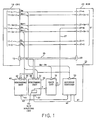
- the data processing system includes a central processing unit (CPU) 10 having an address output port 11 for producing an output address signal.
- the address output port 11 will later be described in detail.
- the output address signal consists of (n + 1) bits arranged from a most significant bit or an n-th bit 2 n to a least significant bit or a zeroth bit 20, where n represents a first predetermined natural number.
- the zeroth through the n-th bits 20 to 2 n of the output address signal are depicted at A0 to A n , respectively.
- the central processing unit 10 further has a CPU input/output port 12 which will later be described in detail.
- the data processing system further comprises a plurality of peripheral units.
- the peripheral units are divided into a specific one and remaining ones which will become clear as the description proceeds.
- the specific one of the peripheral units namely, a specific peripheral unit, is a read-only memory (ROM) 20 which has a memory capacity of 2 n+1 bytes.
- the read-only memory 20 has an ROM address input port 21 for receiving an ROM input address signal.
- the ROM address input port 21 will later be described in detail.
- the ROM input address signal consists of (n + 1) bits arranged from the most significant bit 2 n to the least significant bit 20.
- the ROM address input port 21 is directly supplied with the n bits among the (n + 1) bits of the output address signal as the n bits among the (n + 1) bits of the ROM input address signal.
- the n bits of each of the output and the input address signals are the (n + 1) bits except for an m-th bit 2 m as counted from the least significant bit 20, where m represents a second predetermined natural number which is not greater than the first predetermined natural number.
- the read-only memory 20 has a program memory area (now shown) for memorizing a program which the central processing unit 10 should carry out.
- the read-only memory 20 further has an ROM input/output port 22 and an ROM selection input terminal 23.
- the ROM input/output port 22 is connected to the CPU input/output port 12 through an input/output bus 25. In the manner which will later become clear, the input/output bus 25 is divided into a data bus and a control bus.
- the ROM selection input terminal 23 is for receiving an ROM selection signal which will later become clear.
- the address output port 11 of the central processing unit 10 comprises zeroth through n-th address output terminals 11-0, 11-1, ..., 11-(m-1), 11-m, 11-(m+1), ..., 11-(n-1), and 11-n for producing the zeroth through the n-th bits A0, A1, ..., A m-1 , A m , A m+1 , ..., A n-1 , and A n , respectively.
- the ROM address input port 21 of the read-only memory 20 comprises zeroth through n-th address output terminals 21-0, 21-1, ..., 21-(m-1), 21-m, 21-(m+1), ..., 21-(n-1), and 21-n.
- the zeroth through the (m-1)-th output terminals 21-0 to 21-(m-1) of the ROM address input port 21 are supplied with, as the zeroth through the (m-1)-th bits 20 to 2 m-1 of the ROM input address signal, the zeroth through the (m-1)-th bits A0 to A m-1 from the zeroth through the (m-1)-th address output terminals 11-0 to 11-(m-1) of the address output port 11.
- the (m+1)-th through the n-th output terminals 21-(m+1) to 21-n of the ROM address input port 21 are supplied with, as the (m+1)-th through the n-th bits 2 m+1 to 2 n of the ROM input address signal, the (m+1)-th through the n-th bits A m+1 to A n from the (m+1)-th through the n-th address output terminals 11-(m+1) to 11-n of the address output port 11.
- the m-th output terminal 21-m of the ROM address input port 21 is supplied through a connection line 27 with, as the m-th bit 2 m of the ROM input address signal, a processed bit G which will later become clear.
- the (m+1)-th through the n-th bits A m+1 to A n of the output address signal are supplied to the remaining ones of the peripheral units, namely, remaining peripheral units which are depicted at 30 and 40.
- the remaining peripheral units 30 and 40 have peripheral address input ports 31 and 41 for receiving a combination of the (m+1)-th through the n-th bits A m+1 to A n of the output address signal as a peripheral input address signal.
- the remaining peripheral units 30 and 40 further have peripheral input/output ports 32 and 42 and peripheral selection input terminals 33 and 43.
- the peripheral input/output ports 32 and 42 are connected to the CPU input/output port 12 through the input/output bus 25.
- the peripheral selection input terminals 33 and 43 are for receiving peripheral selection signals which will later become clear.
- peripheral units 30 and 40 may be an input/output device for use as an input/output area or a random access memory (RAM) for use as a work area.
- RAM random access memory
- the output address signal is supplied to an address decoder 50.
- the address decoder 50 decodes the output address signal to produce one of first through third selection signals s1, s2, and s3.
- the first selection signal s1 is delivered to the ROM selection input terminal 23 of the read-only memory 20 as the ROM selection signal.
- the second and the third selection signals s2 and s3 are delivered, as the peripheral selection signals, to the peripheral selection input terminals 33 and 43 of the remaining peripheral units 30 and 40, respectively.
- the output address signal has upper (n - m + 1) bits arranged from the most significant bit 2 n to the m-th bit 2 m .
- the upper (n - m + 1) bits consist with the m-th bit A m to the n-th bit A n .
- the address decoder 50 selects the read-only memory 20 as a selected peripheral unit when the upper (n - m + 1) bits A m to A n are not equal to predetermined bits b m to b n (not shown) arranged from the most significant bit 2 n to the m-th bit 2 m .
- the address decoder 50 selects one of the remaining peripheral units 30 and 40 as the selected peripheral unit.
- the address decoder 50 serves as a peripheral selecting arrangement for selecting one of the peripheral units 20, 30, and 40 as the selected peripheral unit.
- the CPU input/output port 12 of the central processing unit 10 produces an address selection control bit as one of output data.
- the address selection control bit is delivered to the peripheral input/output port 32 of the remaining peripheral unit 30 through the input/output bus 25.
- the remaining peripheral unit 30 includes a bit holding circuit 60 which is supplied with the address selection control bit.
- the bit holding circuit 50 is holding the address selection control bit as a held control bit X.
- the held control bit X is supplied to a gate circuit 70 which is supplied with the upper (n - m + 1) bits A m to A n . Responsive to the held control bit X, the gate circuit 70 processes the m-th bit A m of the output address signal into the processed bit G.
- operation of the gate circuit 70 is conditioned by the predetermined bits b m to b n and a particular bit b x .
- the particular bit b x is equal to the m-th bit 2 m of the predetermined bits, namely, the m-th bit b m .
- the gate circuit 70 produces the m-th bit A m of the output address signal as the processed bit G when the held control bit X is not equal to the particular bit b x .
- the gate circuit 70 produces the m-th bit b m of the predetermined bits as the processed bit G when the held control bit X is equal to the particular bit b x and when the upper (n - m + 1) bits of the output address signal are equal to the predetermined bits except for the m-th bit.
- the gate circuit 70 acts as a bit processing arrangement for processing, in response to the held control bit X, the m-th bit A m of the output address signal into the processed bit G.
- the processed bit G is delivered to the m-th output terminal 21-m of the ROM address input port 21 through the connection line 27 as the m-th bit 2 m of the ROM input address signal. That is, the connection line 27 serves as a bit supplying arrangement for supplying the processed bit G as the m-th bit 2 m of the ROM input address signal to the read-only memory 20.
- the central processing unit 10 is directly capable of accessing an address area of 2 n+1 bytes as a directly-accessible address area.
- the directly-accessible address area is divided into first and second address areas.
- the first address area is an area in which the upper (n - m + 1) bits A m to A n of the output address signal are equal to the predetermined bits b m to b n .
- the second address area is another area in which the upper (n - m + 1) bits A m to A n of the output address signal are not equal to the predetermined bits b m to b n .
- the First address area is assigned to the remaining peripheral units 30 and 40.
- the second address area is assigned to the read-only memory 20.
- the second address area is narrower than the program memory area.
- the central processing unit 10 can not access all of the program memory area.
- the central processing unit 10 can access all of the program memory area by changing the address selection control bit in the manner which will presently be described.
- the central processing unit 10 accesses one of the remaining peripheral units 30 and 40.
- the central processing unit 10 produces the output address signal in which the upper (n - m + 1) bits A m to A n of the output address signal are equal to the predetermined bits b m to b n .
- the address decoder 50 produces one of the second and the third selection signals s2 and s3 that is determined by the zeroth through the (m - 1)-th bits A0 to A m-1 of the output address signal. In other words, the address decoder 50 selects one of the remaining peripheral units 30 and 40 as the selected peripheral unit.
- the program memory area of the read-only memory 20 is divided into first, second, and third memory areas.
- the first memory area is an area where the m-th through the n-th bits of the ROM input address signal are equal to the predetermined bits b m to b n .
- the second memory area is another area where the m-th through the n-th bits of the ROM input address signal are equal to the predetermined bits b m to b n except for the m-th bit 2 m .
- the third memory area is a remaining area equal to combination of areas which are other than the first and the second memory areas among the program memory area.
- the central processing unit 10 accesses the second and the third memory areas of the program memory area of the read-only memory 20.
- the central processing unit 10 produces the address selection control bit which is not equal to the particular bit b x .
- the bit holding circuit 60 holds the address selection control bit as the held control bit X.
- the central processing unit 10 produces the output address signal in which the upper (n - m + 1) bits A m to A n of the output address signal are not equal to the predetermined bits b m to b n .
- the address decoder 50 selects the read-only memory 20 as the selected peripheral unit.
- the gate circuit 70 produces the m-th bit A m of the output address signal as the processed bit G. Accordingly, the read-only memory 20 is supplied with the output address signal as the input address signal.
- the central processing unit 10 accesses the first and the third memory areas of the program memory area of the read-only memory 20.
- the central processing unit 10 produces the address selection control bit which is equal to the particular bit b x .
- the bit holding circuit 60 holds the address selection control bit as the held control bit X.
- the central processing unit 10 produces the output address signal in which the upper (n - m + 1) bits of the output address signal are not equal to the predetermined bits. Responsive to the output address signal, the address decoder 50 selects the read-only memory 20 as the selected peripheral unit.
- the central processing unit 10 produces the output address signal in which the upper (n - m + 1) bits of the output address signal are equal to the predetermined bits except for the m-th bit.
- the gate circuit 70 produces the m-th bit b m of the predetermined bits as the processed bit G.
- the read-only memory 20 is supplied with the input address signal equal to the output address signal except for the m-th bit 2 m . That is, the output address signal is supplied to the read-only memory 20 as the input address signal with the m-th bit b m of the predetermined bits substituted for the m-th bit A m of the output address signal.
- the central processing unit 10 can access not only the remaining peripheral units 30 and 40 but also the first and the third memory areas of the program memory area of the read-only memory 20.
- the central processing unit 10 is capable of accessing all of the program memory area of the read-only memory 20.
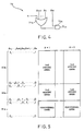
- Fig. 2 shows an example of the gate circuit 70.
- each of the predetermined bits b m to b n has a logic one value.
- the particular bit b x has a logic one value.
- the gate circuit 70 comprises an AND circuit 71 and an OR circuit 72.
- the AND circuit 71 carries out an AND operation on the held control bit X and the (n - m) bits of the upper (n - m + 1) bits except for the m-th bit A m , namely, A m+1 to A n to produce an AND'ed bit.
- the OR circuit 72 carries out an OR operation on the AND'ed bit and the m-th bit A m of the upper (n - m + 1) bits to produce an OR'ed bit as the processed bit G.
- Fig. 3 shows an address space which the central processing unit 10 can use when the gate circuit 70 shown in Fig. 2 is employed.
- the address space is divided into first, second, and third partial address spaces 81, 82, and 83.
- the first partial address space 81 is a space where each of the upper (n - m + 1) bits A m to A n of the output address signal has a logic one value.
- the zeroth through the (m-1)-th bits A0 to A m-1 are variable.
- the second partial address space 82 is another space where each of the (n - m) bits A m+1 to A n of the upper (n - m + 1) bits has a logic one value and the m-th bit A m of the upper (n - m + 1) bits has a logic zero value.
- the third partial address space 83 is a remaining space equal to combination of spaces which are other than the first and the second partial address spaces 81 and 82 among the address space of the central processing unit 10.
- the third partial address space 83 is mapped into the third memory area of the program memory area of the read-only memory 20 no matter whether the held control bit X has the logic zero value or the logic one value.
- the second partial address space 82 is mapped into the second memory area of the program memory area of the read-only memory 20 when the held control bit X has the logic zero value.
- the second partial address space 82 is mapped into the first memory area of the program memory area of the read-only memory 20 when the held control bit X has the logic one value.
- Fig. 4 shows another example of the gate circuit 70.
- each of the predetermined bits b m to b n has a logic zero value.
- the particular bit b x has a logic zero value.
- the gate circuit 70 comprises an OR circuit 71a and an AND circuit 72a.
- the OR circuit 71a carries out an OR operation on the held control bit X and the (n - m) bits of the upper (n - m + 1) bits except for the m-th bit A m , namely, A m+1 to A n to produce an OR'ed bit.
- the AND circuit 72a carries out an AND operation on the OR'ed bit and the m-th bit A m of the upper (n - m + 1) bits to produce an AND'ed bit as the processed bit G.
- Fig. 5 shows an address space which the central processing unit 10 can use when the gate circuit 70 shown in Fig. 4 is employed.
- the address space is divided into first, second, and third partial address spaces 81a, 82a, and 83a.
- the first partial address space 81a is a space where each of the upper (n - m + 1) bits A m to A n of the output address signal has a logic zero value.
- the second partial address space 82a is another space where each of the (n - m) bits A m+1 to A n of the upper (n - m + 1) bits has a logic zero value and the m-th bit A m of the upper (n - m + 1) bits has a logic one value.
- the third partial address space 83a is a remaining space equal to a space which is other than the first and the second partial address spaces 81a and 82a among the address space of the central processing unit 10.
- the first partial address space 81a is mapped into the peripheral area no matter whether the held control bit X has the logic one value of the logic zero value.
- the third partial address space 83a is mapped into the third memory area of the program memory area of the read-only memory 20 no matter whether the held control bit X has the logic one value of the logic zero value.
- the second partial address space 82a is mapped into the second memory area of the program memory area of the read-only memory 20 when the held control bit X has the logic one value.
- the second partial address space 82a is mapped into the first memory area of the program memory area of the read-only memory 20 when the held control bit X has the logic zero value.
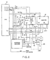
- Fig. 6 shows an example of the data processing system according to this invention that is control equipment for use in an automobile telephone terminal.
- the first predetermined natural number n is equal to fifteen.
- the second predetermined natural number m is equal to thirteen. It is assumed that each of the predetermined bits b13 to b15 has the logic one value and the particular bit b x has the logic one value.
- the remaining peripheral unit 40 is the random access memory (RAM) for use as the work area.
- the input/output bus 25 is divided into the data bus and the control bus which are depicted at 25-1 and 25-2, respectively.
- the central processing unit 10 delivers a read-out instruction signal RD and a write-in instruction signal WR to the control bus 25-2.
- the central processing unit 10 also delivers the address selection control bit depicted at AS to the bit holding circuit 60 through the data bus 25-1.
- the central processing unit 10 receives an interruption signal INT from one of input/output (I/O) devices (not shown) which are the remaining peripheral units.
- a combination of the input/output devices is for use as an input/output area.
- the read-only memory 20 has the memory capacity of 64 Kbytes.
- the random access memory has a memory capacity of 8 Kbytes.
- the bit holding circuit 60 comprises a type D flip-flop 61 and an NOR circuit 62. Responsive to the write-in instruction signal WR supplied from the central processing unit 10 and to the second selection signal s2 supplied from the address decoder 50, the NOR circuit 62 produces a holding instruction signal. Responsive to the holding instruction signal, the type D flip-flop 61 holds the address selection control bit AS as the held control bit X. Supplied with a reset signal RST, the type D flip-flop 61 produces the held control bit X having the logic zero value.
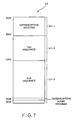
- the program memory area of the read-only memory 20 is divided into the first, the second, and the third memory areas which are depicted at 20-1, 20-2, and 20-3, respectively.
- the first memory area 20-1 is indicated by an address extent which is between hexadecimal E000 and hexadecimal FFFF.
- the first memory area 20-1 memorizes an interruption routine.
- the second memory area 20-2 is indicated by another extent which is between hexadecimal C000 and hexadecimal DFFF.
- the second memory area 20-2 memorizes a first sequence.
- the third memory area 20-3 is indicated by a remaining extent which ranges from hexadecimal 0000 to hexadecimal BFFF.
- the third memory area 20-3 memorizes a second sequence and an interruption start program which is memorized in a memory address of hexadecimal 0038.
- the first partial address space 81 is indicated by an address extent ranging from hexadecimal E000 to hexadecimal FFFF.
- the first partial address space 81 is divided into first and second portions 81-1 and 81-2.
- the first portion 81-1 is indicated by an address extent between hexadecimal F800 and hexadecimal FFFF.
- the second portion is indicated by another address extent between hexadecimal E000 and hexadecimal E7FF.
- the first portion 81-1 of the first partial address space 81 is mapped into the input/output area no matter whether the held control bit X has the logic zero value or the logic one value.
- the second portion 81-2 of the first partial address space 81 is mapped into the work area no matter whether the held control bit X has the logic zero value or the logic one value.
- the third partial address space 83 is indicated by an address extent between hexadecimal 0000 and hexadecimal BFFF.
- the third partial address space 83 is mapped into the third memory area 20-3 for the second sequence and the interruption start program no matter whether the held control bit X has the logic zero value or the logic one value.
- the second partial memory area 20-2 is indicated by an address extent between hexadecimal C000 and hexadecimal DFFF.
- the second partial memory area 20-2 is mapped into the second memory area 20-2 for the first sequence when the held control bit X has the logic zero value.
- the second partial memory area 20-2 is mapped into the first memory area 20-1 for the interruption routine when the held control bit X has the logic one value.
- the bit holding circuit 60 produces the held control bit X having the logic zero value.
- the central processing unit 10 can access only a combination of the second and the third memory areas 20-2 and 20-3 of the program area of the read-only memory 20.
- the central processing unit 10 receives the interruption signal INT from one of the input/output devices at a first stage S1
- the central processing unit 10 produces the output address signal indicative of an address of hexadecimal 0038.
- the read-only memory 20 delivers the interruption start program to the central processing unit 10 through the data bus 25-1.
- the central processing unit 10 sends the address selection control bit AS of logic one value to the bit holding circuit 60.
- the bit holding circuit 60 produces the held control bit X having the logic one value at a second stage S2.
- the central processing unit 10 calls the interruption routine at a third stage S3 and executes the interruption routine at a fourth stage S4.
- the central processing unit 10 controls the bit holding circuit 60 to make the bit holding circuit 60 produce the held control bit X having the logic zero value at a fifth stage S5. Thereafter, the process returns to a point of one of the first and the second sequences at which the interruption occurs at a sixth stage S6.
- the gate circuit 70 illustrated in Fig. 1 may process one of the upper (n- m + 1) bits of the output address signal except for the m-th bit into the processed bit.
- gate circuit 70 may process a plurality of bits of the output address signal into a plurality of processed bits which are supplied to the read-only memory 20.
Landscapes
- Engineering & Computer Science (AREA)
- Theoretical Computer Science (AREA)
- Physics & Mathematics (AREA)
- General Engineering & Computer Science (AREA)
- General Physics & Mathematics (AREA)
- Storage Device Security (AREA)
- Communication Control (AREA)
Claims (5)
- Datenverarbeitungssystem mit einer zentralen Verarbeitungseinheit (10) zum Erzeugen eines Ausgabeadreßsignals (A₀-An), das aus n+1 Bits besteht, die von einem hochwertigsten Bit 2n zu einem niederwertigsten Bit 2⁰ angeordnet sind, wobei n eine erste vorgegebene natürliche Zahl darstellt, einer speziellen Periphereinheit (20) zum Empfangen eines Eingabeadreßsignals (21), das aus n+1 Bits besteht, die von dem hochwertigsten Bit 2n zum niederwertigsten Bit 2⁰ angeordnet sind, anderen Periphereinheiten (30,40), einer mit der zentralen Verarbeitungseinheit (10) und mit der speziellen Periphereinheit (20) und den anderen Periphereinheiten verbundenen Peripherauswahleinrichtung (50), um als Antwort auf das Ausgabeadreßsignal unter der speziellen Periphereinheit (20) und den anderen Periphereinheiten (30,40) eine bestimmte als ausgewählte Periphereinheit auszuwählen, einer mit der zentralen Verarbeitungseinheit (10) verbundenen Bitverarbeitungseinrichtung (70) zum Verarbeiten bestimmter Bits des Ausgabeadreßsignals in ein verarbeitetes Bit, dadurch gekennzeichnet, daß von den n+1 Bits des Ausgabeadreßsignals die spezielle Periphereinheit (20) mit n Bits versorgt wird, die n Bits der n+1 Bits des Eingabeadreßsignals bilden, wobei sich n Bits der n+l Bits des Ausgabe- und Eingabeadreßsignals jeweils entsprechen, mit Ausnahme eines m-ten Adreßbits 2m, gezählt vom niederwertigsten Bit 2⁰, wobei m eine zweite vorgegebene natürliche Zahl darstellt, die kleiner als die erste vorgegebene natürliche Zahl ist, wobei das Datenverarbeitungssystem ferner dadurch gekennzeichnet ist, daß es eine Bithalte-Einrichtung (60) zum Halten eines von der zentralen Verarbeitungseinheit (10) erzeugten Adreßauswahl-Steuerbits als gehaltenes Steuerbit (X) und eine mit der Bitverarbeitungseinrichtung (70) und der speziellen Periphereinheit (20) verbundene Bitzuführungseinrichtung (27) zum Zuführen eines von der Bitverarbeitungseinheit (70) als m-tes Adreßbit 2m des Eingabeadreßsignals erzeugten, verarbeiteten Bits (G) zu der speziellen Periphereinheit (20) aufweist, wobei die Peripherauswahleinheit (50) unter den anderen Periphereinheiten (30,40) eine bestimmte als die ausgewählte Periphereinheit auswählt, wenn alle Bits vom m-ten Adreßbit 2m zum hochwertigsten Adreßbit 2n des Ausgabeadreßsignals einen ersten Binärwert haben, und die Peripherauswahleinrichtung (50) die spezielle Periphereinheit (20) als ausgewählte Periphereinheit auswählt, wenn nicht alle Bits vom m-ten Adreßbit 2m zum hochwertigsten Adreßbit 2n des Ausgabeadreßsignals den ersten Binärwert haben, wobei die Bitverarbeitungseinrichtung (70) mit der Bithalte-Einrichtung (60) verbunden ist und mit dem m-ten bis n-ten Adreßbit 2m bis 2n des Ausgabeadreßsignals als die bestimmten Bits des Ausgabeadreßsignals versorgt wird, wobei, wenn durchgehend vom m+1-ten bis zum n-ten alle Adreßbits 2m+1 bis 2n des Ausgabeadreßsignals den ersten Binärwert haben und das m-te Adreßbit 2m des Ausgabeadreßsignals einen zweiten, vom ersten Binärwert verschiedenen Binärwert hat, die Bitverarbeitungseinrichtung (70) das verarbeitete Bit (G) mit einem Wert gleich dem des zweiten Binärwerts ausgibt, wenn das gehaltene Steuerbit (X) den zweiten Binärwert hat und das verarbeitete Bit (G) mit einem Wert gleich dem des ersten Binärwerts ausgibt, wenn das gehaltene Steuerbit (X) den ersten Binärwert hat.
- Datenverarbeitungssystem nach Anspruch 1, dadurch gekennzeichnet, daß die Bithalte-Einrichtung (60) in einer bestimmten (30) der anderen Periphereinheiten enthalten ist.
- Datenverarbeitungssystem nach Anspruch 1, dadurch gekennzeichnet, daß die spezielle Periphereinheit (20) ein Festspeicher ist.
- Datenverarbeitungssystem nach Anspruch 1, dadurch gekennzeichnet, daß der erste bzw. der zweite Binärwert den Wert logisch Eins bzw. logisch Null hat, die Bitverarbeitungseinrichtung (70) einen UND-Schaltkreis (71), um mit dem gehaltenen Steuerbit (X) und den m+1-ten bis n-ten Adreßbits 2m+1 bis 2n des Ausgabeadreßsignals eine UND-Operation auszuführen, um ein erstes UND-verknüpftes Bit zu erzeugen und einen ODER-Schaltkreis (72) aufweist, um mit dem ersten UND-verknüpften Bit und dem m-ten Adreßbit 2m des Ausgabeadreßsignals eine ODER-Operation auszuführen, um ein erstes ODER-verknüpftes Bit als verarbeitetes Bit (G) zu erzeugen.
- Datenverarbeitungssystem nach Anspruch 1, dadurch gekennzeichnet, daß der erste bzw. der zweite Binärwert den Wert logisch Null bzw. logisch Eins hat, die Bitverarbeitungseinrichtung (70) einen ODER-Schaltkreis (71a), um mit dem gehaltenen steuerbit (X) und den m+1-ten bis n-ten Adreßbits 2m+1 bis 2n des Ausgabeadreßsignals eine ODER-Operation auszuführen, um ein zweites ODER-verknüpftes Bit zu erzeugen und einen UND-Schaltkreis (72a) aufweist, um mit dem zweiten ODER-verknüpften Bit und dem m-ten Adreßbit 2m des Ausgabeadreßsignals eine UND-Operation auszuführen, um ein zweites UND-verknüpftes Bit als verarbeitetes Bit (G) zu erzeugen.
Applications Claiming Priority (2)
| Application Number | Priority Date | Filing Date | Title |
|---|---|---|---|
| JP26994788A JPH077353B2 (ja) | 1988-10-26 | 1988-10-26 | アドレス選択方式 |
| JP269947/88 | 1988-10-26 |
Publications (3)
| Publication Number | Publication Date |
|---|---|
| EP0366458A2 EP0366458A2 (de) | 1990-05-02 |
| EP0366458A3 EP0366458A3 (de) | 1991-04-17 |
| EP0366458B1 true EP0366458B1 (de) | 1995-06-28 |
Family
ID=17479424
Family Applications (1)
| Application Number | Title | Priority Date | Filing Date |
|---|---|---|---|
| EP19890311039 Expired - Lifetime EP0366458B1 (de) | 1988-10-26 | 1989-10-26 | Datenverarbeitungsanordnung, in welcher eine einfache Peripheriesteuerungseinrichtung es einer zentralen Verarbeitungseinheit ermöglicht, auf einen erweiterten Adressbereich zuzugreifen |
Country Status (3)
| Country | Link |
|---|---|
| EP (1) | EP0366458B1 (de) |
| JP (1) | JPH077353B2 (de) |
| AU (1) | AU615587B2 (de) |
Families Citing this family (2)
| Publication number | Priority date | Publication date | Assignee | Title |
|---|---|---|---|---|
| CA2003821C (en) * | 1989-04-20 | 1996-12-03 | Richard J. Molnar | Process controller single memory chip shadowing technique |
| JP4771609B2 (ja) * | 2000-05-08 | 2011-09-14 | フルタ電機株式会社 | 空気清浄機付きプランター |
-
1988
- 1988-10-26 JP JP26994788A patent/JPH077353B2/ja not_active Expired - Lifetime
-
1989
- 1989-10-26 AU AU43808/89A patent/AU615587B2/en not_active Ceased
- 1989-10-26 EP EP19890311039 patent/EP0366458B1/de not_active Expired - Lifetime
Also Published As
| Publication number | Publication date |
|---|---|
| AU4380889A (en) | 1990-05-03 |
| JPH077353B2 (ja) | 1995-01-30 |
| JPH02116939A (ja) | 1990-05-01 |
| EP0366458A2 (de) | 1990-05-02 |
| AU615587B2 (en) | 1991-10-03 |
| EP0366458A3 (de) | 1991-04-17 |
Similar Documents
| Publication | Publication Date | Title |
|---|---|---|
| US4654781A (en) | Byte addressable memory for variable length instructions and data | |
| US4373181A (en) | Dynamic device address assignment mechanism for a data processing system | |
| US6401155B1 (en) | Interrupt/software-controlled thread processing | |
| US4713759A (en) | Memory bank switching apparatus | |
| US5806082A (en) | Wrap-around mechanism for memory split-wordline read | |
| US6226736B1 (en) | Microprocessor configuration arrangement for selecting an external bus width | |
| WO1998049623A1 (en) | Memory access protection | |
| US5109334A (en) | Memory management unit capable of expanding the offset part of the physical address | |
| WO1990004576A2 (en) | Automatically variable memory interleaving system | |
| KR890002469B1 (ko) | 마이크로컴퓨터의 기억 페이징 시스템 | |
| US4413315A (en) | Addressing system | |
| WO1997045870A1 (en) | A microcontroller having an n-bit data bus width with less than n i/o pins and a method therefor | |
| US5537576A (en) | Expandable memory for a digital signal processor including mapped first and second memory banks forming a continuous and contiguous address space | |
| GB2024475A (en) | Memory access controller | |
| US5127096A (en) | Information processor operative both in direct mapping and in bank mapping, and the method of switching the mapping schemes | |
| US4764896A (en) | Microprocessor assisted memory to memory move apparatus | |
| EP0366458B1 (de) | Datenverarbeitungsanordnung, in welcher eine einfache Peripheriesteuerungseinrichtung es einer zentralen Verarbeitungseinheit ermöglicht, auf einen erweiterten Adressbereich zuzugreifen | |
| US5373467A (en) | Solid state memory device capable of providing data signals on 2N data lines or N data lines | |
| US4947396A (en) | Method and system for detecting data error | |
| US4388707A (en) | Memory selecting system | |
| US5388239A (en) | Operand address modification system | |
| GB2108737A (en) | Byte addressable memory for variable length instructions and data | |
| JPS6232516B2 (de) | ||
| JPS59231625A (ja) | アドレス設定方式 | |
| JP2918570B2 (ja) | 中央演算処理装置 |
Legal Events
| Date | Code | Title | Description |
|---|---|---|---|
| PUAI | Public reference made under article 153(3) epc to a published international application that has entered the european phase |
Free format text: ORIGINAL CODE: 0009012 |
|
| 17P | Request for examination filed |
Effective date: 19891124 |
|
| AK | Designated contracting states |
Kind code of ref document: A2 Designated state(s): FR GB SE |
|
| PUAL | Search report despatched |
Free format text: ORIGINAL CODE: 0009013 |
|
| AK | Designated contracting states |
Kind code of ref document: A3 Designated state(s): FR GB SE |
|
| 17Q | First examination report despatched |
Effective date: 19931214 |
|
| GRAA | (expected) grant |
Free format text: ORIGINAL CODE: 0009210 |
|
| AK | Designated contracting states |
Kind code of ref document: B1 Designated state(s): FR GB SE |
|
| ET | Fr: translation filed | ||
| PLBE | No opposition filed within time limit |
Free format text: ORIGINAL CODE: 0009261 |
|
| STAA | Information on the status of an ep patent application or granted ep patent |
Free format text: STATUS: NO OPPOSITION FILED WITHIN TIME LIMIT |
|
| 26N | No opposition filed | ||
| PGFP | Annual fee paid to national office [announced via postgrant information from national office to epo] |
Ref country code: SE Payment date: 19971009 Year of fee payment: 9 |
|
| PG25 | Lapsed in a contracting state [announced via postgrant information from national office to epo] |
Ref country code: SE Free format text: LAPSE BECAUSE OF NON-PAYMENT OF DUE FEES Effective date: 19981027 |
|
| EUG | Se: european patent has lapsed |
Ref document number: 89311039.5 |
|
| PGFP | Annual fee paid to national office [announced via postgrant information from national office to epo] |
Ref country code: FR Payment date: 20011010 Year of fee payment: 13 |
|
| PGFP | Annual fee paid to national office [announced via postgrant information from national office to epo] |
Ref country code: GB Payment date: 20011024 Year of fee payment: 13 |
|
| REG | Reference to a national code |
Ref country code: GB Ref legal event code: IF02 |
|
| PG25 | Lapsed in a contracting state [announced via postgrant information from national office to epo] |
Ref country code: GB Free format text: LAPSE BECAUSE OF NON-PAYMENT OF DUE FEES Effective date: 20021026 |
|
| GBPC | Gb: european patent ceased through non-payment of renewal fee | ||
| PG25 | Lapsed in a contracting state [announced via postgrant information from national office to epo] |
Ref country code: FR Free format text: LAPSE BECAUSE OF NON-PAYMENT OF DUE FEES Effective date: 20030630 |
|
| REG | Reference to a national code |
Ref country code: FR Ref legal event code: ST |