EP0366282A2 - Hohlgehäuse - Google Patents
Hohlgehäuse Download PDFInfo
- Publication number
- EP0366282A2 EP0366282A2 EP89310097A EP89310097A EP0366282A2 EP 0366282 A2 EP0366282 A2 EP 0366282A2 EP 89310097 A EP89310097 A EP 89310097A EP 89310097 A EP89310097 A EP 89310097A EP 0366282 A2 EP0366282 A2 EP 0366282A2
- Authority
- EP
- European Patent Office
- Prior art keywords
- cavity
- operative element
- silicone gel
- deposit
- secured
- Prior art date
- Legal status (The legal status is an assumption and is not a legal conclusion. Google has not performed a legal analysis and makes no representation as to the accuracy of the status listed.)
- Granted
Links
Images
Classifications
-
- H—ELECTRICITY
- H10—SEMICONDUCTOR DEVICES; ELECTRIC SOLID-STATE DEVICES NOT OTHERWISE PROVIDED FOR
- H10W—GENERIC PACKAGES, INTERCONNECTIONS, CONNECTORS OR OTHER CONSTRUCTIONAL DETAILS OF DEVICES COVERED BY CLASS H10
- H10W76/00—Containers; Fillings or auxiliary members therefor; Seals
- H10W76/40—Fillings or auxiliary members in containers, e.g. centering rings
- H10W76/42—Fillings
- H10W76/47—Solid or gel fillings
-
- H—ELECTRICITY
- H10—SEMICONDUCTOR DEVICES; ELECTRIC SOLID-STATE DEVICES NOT OTHERWISE PROVIDED FOR
- H10W—GENERIC PACKAGES, INTERCONNECTIONS, CONNECTORS OR OTHER CONSTRUCTIONAL DETAILS OF DEVICES COVERED BY CLASS H10
- H10W74/00—Encapsulations, e.g. protective coatings
- H10W74/40—Encapsulations, e.g. protective coatings characterised by their materials
- H10W74/47—Encapsulations, e.g. protective coatings characterised by their materials comprising organic materials, e.g. plastics or resins
- H10W74/476—Organic materials comprising silicon
-
- H—ELECTRICITY
- H10—SEMICONDUCTOR DEVICES; ELECTRIC SOLID-STATE DEVICES NOT OTHERWISE PROVIDED FOR
- H10W—GENERIC PACKAGES, INTERCONNECTIONS, CONNECTORS OR OTHER CONSTRUCTIONAL DETAILS OF DEVICES COVERED BY CLASS H10
- H10W90/00—Package configurations
- H10W90/701—Package configurations characterised by the relative positions of pads or connectors relative to package parts
- H10W90/751—Package configurations characterised by the relative positions of pads or connectors relative to package parts of bond wires
- H10W90/756—Package configurations characterised by the relative positions of pads or connectors relative to package parts of bond wires between a chip and a stacked lead frame, conducting package substrate or heat sink
Definitions
- This invention is concerned with cavity packages.
- cavity package where used herein embraces articles in the form of a package within which an operative element, for example a semiconductor, integrated circuit or other electronic device, is contained.
- Power packages are well known in the art and formerly were made by moulding a thermosetting material onto the operative element. More recently, it has been proposed to employ packages which comprise a package body premoulded from a thermoplastic material and having a bore or cavity extending through the thickness of the body and in which the operative element is contained.
- the thermoplastic material may be, for example, polyphenylsulphone or polybutylterephthalate and the package may comprise a heat sink and a metal lead frame for electrical and/or thermal connection of the operative element to other devices.
- a silicon die or semiconductor chip or other operative element may be bonded into the cavity which may then be partially filled with a deposit of a silicone composition which cures to provide a layer of a soft and self-sealing silicone gel.
- a lid, for example of polyphenylsulphone may be secured in the cavity over the gel for example by an adhesive bonding agent.
- the operative element in a package as just above referred to is protected by the gel against effects of atmospheric humidity and contaminants present in the atmosphere.
- the packages are thus commercially acceptable in many respects.
- the silicone gel-forming compositions used have wetting and flow characteristics such that the gel layer develops a concave meniscus and thus the amount of gel covering the operative element at the centre of the cavity is limited, resulting in a tendency to fill the cavity to an extent such that the edge portions of the layer interfere with correct positioning of the lid.
- Attempts have been made to overcome this difficulty using various techniques, for example adjustment of the viscosity or cure speed of the deposit of silicone composition, variation of the temperature at which the deposit is applied or cured, variation of the application pressure of the deposit and preheating of the package body. Whilst some control of the flow and seepage of the deposit may be achieved by use of such techniques nevertheless it remains a problem to maximise the filling of the available space in the cavity by the gel whilst limiting interference of the gel with the location of the lid.
- an improved disposition of the gel in the package body of a cavity package of the type referred to above may be achieved by application of a coating of a surface-active composition comprising a fluorine compound on heightwise extending edge portions of the cavity, at that end of the cavity which is adjacent a surface of the package body to which the lid is to be attached, prior to application of the deposit of silicone gel-forming composition to cover the operative element.
- the present invention provides in one of its aspects a method of making a cavity package which comprises procuring a package body having a cavity within which an operative element is located and having a securing surface to which a lid may be secured, and applying onto the operative element in the cavity a deposit of a silicone gel-forming composition to cover the operative element with a layer of desired thickness of silicone gel characterised in that prior to application of the deposit of silicone gel-forming composition to cover the operative element a coating of a surface-active composition comprising a fluorine compound is formed on surfaces of the cavity at that end of the cavity which is adjacent the securing surface of the package body and which extend heightwise of the operative element when the deposit of silicone gel is applied thereto.
- the package body may be formed by injection moulding a thermoplastic material for example polyphenylsulphone to any desired shape and thickness.
- the shape and thickness may be dictated by the intended location of the cavity package in apparatus of which it is intended to form a part in juxtaposition to other parts. Conveniently it is in the form of a cuboid and may have a metal lead frame comprising several metal connectors extending from one or more of its side surfaces.
- the package body incorporates a cavity in which, in the completed package, the operative element is positioned below the layer of gel. Surfaces of the package body defining the cavity thus extend heightwise with respect to the gel covered operative element.
- the cavity may be provided in a bore extending through the thickness of the package body.
- the securing surface of the block may be an outer surface of the block adjacent the mouth of the bore, or may be provided by a lip formed in the bore at a depth such that an outer surface of the lid may be coplanar with the outer surface of the block.
- the operative element may be a silicon die or semiconductor chip or other element and may be secured e.g. by adhesive to a heat sink secured to the block.
- the package body consists of a rectangular block of substantially uniform thickness moulded from polyphenylsulphone resin; the cavity is part of a stepped bore which extends heightwise through the thickness of the block and opens into an enlarged upper portion of the bore in which the securing surface is provided; the operative element is a silicon semiconductor chip and is mounted on a heat sink secured in an enlarged lower portion of the bore; and metal lead frames for electrical and/or thermal connection of the operative element to other devices extend from two side surfaces of the block and are connected to the operative element.
- the coating of surface-active composition is formed on heightwise extending edge portions of the cavity at that end of the cavity which is adjacent the securing surface of the package body.
- a lower edge of the coating is located so that flow of the gel up the walls of the cavity is restricted, whereby to induce the gel to adopt a somewhat convex meniscus.
- the non-concave nature of the upper surface of the cured gel layer is important to production of an improved disposition of the gel over the operative element at the centre of the cavity without encroachment of edge portions of the layer of gel onto the securing surfaces. It is an important feature of the present invention that the lower edge of the coating is precisely defined.
- the upper edge of the coating is clearly defined in order that it does not interfere with securing of a lid to the package body. If necessary, gel which has encroached onto the securing surface may subsequently be removed using solvent.
- Suitable techniques include printing and stamping.
- the viscosity of the surface active composition is suitably adjusted with solvents and/or extenders in accordance with the application technique to be used for application of the coating to the cavity walls and in accordance with the fact that a uniform coating is required on defined areas of a surface which may be vertical at the time of application.
- the surface-active composition may thus comprise the fluorine compound alone or in conjunction with solvents, for example volatile alcohols e.g. isopropanol or fluorocarbons e.g. chlorofluorohydrocarbons and/or other materials.
- the fluorine compound may comprise a fluorinated aliphatic material of the type known to have surfactant properties.
- the fluorine compound is preferably a non-ionic material and may be for example a fluorinated alkyl ester.
- Preferred fluorine compounds are fluoroaliphatic copolymers, the most preferred being those which polymerise readily at room or elevated temperature.
- a preferred fluorine compound is poly(1H,1H-pentadecylfluorooctylmethacrylate).
- the silicone gel-forming composition may be any of those commercially available materials having the required degree of purity for semiconductor applications.
- Silicone gel-forming compositions have been known for many years. They can be cured to provide non-elastomeric materials characterised by low physical strength as demonstrated by poor tear strength, elongation and tensile strength and low hardness. They are neither solid nor liquid and usually flow under pressure. These materials have been described in several patent specifications, for example G.B.
- a metered amount of the silicone gel-forming composition is applied as a deposit in the cavity on top of the operative element.
- the amount metered is sufficient to cover the operative element with a layer of desired thickness and to flow into the lower confines of the cavity.
- the deposit is cured, for example at 150°C for 30 minutes.
- the silicone composition settles and edge portions of the layer creep upwards in contact with the heightwise extending walls of the cavity, their upward movement is checked by the coating of surfactant on the wall surface, but the centre of the deposit may continue to rise so that the layer has a somewhat convex meniscus thus ensuring that an adequate depth of the layer exists above the operative element without the silicone contaminating the securing surface of the package.
- a lid may be secured to the block in any suitable fashion, for example by ultrasonic techniques or by use of suitable adhesives for example those based on silicone, epoxy resins or polyurethanes.
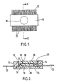
- the cavity package shown in the drawings comprises a rectangular block (10) of substantially uniform thickness moulded from polyphenylsulphone.
- a stepped bore (12) extends heightwise (as viewed in Figure 2) through the thickness of the block and is wider at its open ends than at its mid region.
- An upper end of the bore has a lip (14) which provides a securing surface of the block adjacent to the upper surface of the block (as viewed in Figure 2).
- a lid (16) is secured to the lip with its upper surface flush with the upper surface of the block (10).
- the lower portion of the bore is shaped to receive a heat sink (18) which is bonded in place with adhesive.
- a silicon semiconductor chip (20) is adhesively bonded to the heat sink.
- Metal lead frames (22) for electrical and/or thermal connection of the operative element to other devices are connected to the semiconductor chip by leads (24) and extend from opposite side surfaces of the block.
- a layer of silicone gel (26) is located on and around the semiconductor chip (20) and the leads (24), in the cavity defined by the heightwise extending walls of the bore (12) below the lip (14), and by the heat sink (18).
- a coating of a surface-active composition designated Fluorad® Surface Modifier FC-723 which is understood to be a 0.2% solution of poly(1H,1H-pentadecylfluorooctylmethacrylate) in fluorocarbon solvents, was applied as a narrow circular band (30) around the inner surfaces of the bore by stamping it onto heightwise extending edge portions (30) of the cavity just below (as viewed in Figure 2) the lip (14) i.e. at that end of the cavity which is adjacent the securing surface of the package body.
- a lower edge of the coating was located at a level to be above the semiconductor chip but below the lip (14) as viewed in Figure 2.
- the coating was allowed to dry at room temperature.
- the heat sink (18) with the semiconductor chip (20) bonded thereto was adhesively bonded to the block in the position shown in Figure 2.
- a deposit of a silicone gel-forming composition was metered into the cavity on top of the semiconductor chip (20), the heat sink (18) and the leads (24).
- the silicone gel-forming composition was formed by mixing components comprising 99 parts by weight of a dimethylvinylsiloxy end-blocked polydimethylsiloxane having a viscosity of about 450 mm2/s, 0.4 part by weight of a low molecular weight branched polysiloxane containing Me2SiO and MeViSiO units (where Me represents a methyl group and Vi represents a vinyl group), 0.8 part by weight of a polysiloxane consisting of Me2SiO, MeHSiO and Me3SiO units and having a viscosity of about 5 mm2/s, and 0.2 part of a platinum containing catalyst for the SiH, SiVi addition reaction.
- the assembly was placed in an oven heated to 150°C for 30 minutes to cure the silicone gel. It was found that the layer of cured gel had a convex meniscus (28) and that its edge portions had not encroached onto the lip (14). The lid was adhesively bonded in place.
Landscapes
- Structures Or Materials For Encapsulating Or Coating Semiconductor Devices Or Solid State Devices (AREA)
- Compositions Of Macromolecular Compounds (AREA)
- Encapsulation Of And Coatings For Semiconductor Or Solid State Devices (AREA)
- Paints Or Removers (AREA)
Applications Claiming Priority (2)
| Application Number | Priority Date | Filing Date | Title |
|---|---|---|---|
| GB8825201 | 1988-10-27 | ||
| GB888825201A GB8825201D0 (en) | 1988-10-27 | 1988-10-27 | Cavity packages |
Publications (3)
| Publication Number | Publication Date |
|---|---|
| EP0366282A2 true EP0366282A2 (de) | 1990-05-02 |
| EP0366282A3 EP0366282A3 (de) | 1991-07-17 |
| EP0366282B1 EP0366282B1 (de) | 1994-11-30 |
Family
ID=10645897
Family Applications (1)
| Application Number | Title | Priority Date | Filing Date |
|---|---|---|---|
| EP89310097A Expired - Lifetime EP0366282B1 (de) | 1988-10-27 | 1989-10-03 | Hohlgehäuse |
Country Status (4)
| Country | Link |
|---|---|
| EP (1) | EP0366282B1 (de) |
| JP (1) | JPH02183546A (de) |
| DE (1) | DE68919648T2 (de) |
| GB (1) | GB8825201D0 (de) |
Cited By (4)
| Publication number | Priority date | Publication date | Assignee | Title |
|---|---|---|---|---|
| FR2676595A1 (fr) * | 1991-05-16 | 1992-11-20 | Dow Corning Gmbh | Procede de formation d'un revetement protecteur sur un dispositif a semi-conducteur. |
| EP0939440A3 (de) * | 1998-02-25 | 2000-05-03 | Shin-Etsu Chemical Co., Ltd. | Verfahren zur Herstellung einer Halbleiterverpackung und dazu verwendete Organopolysiloxanverbindung |
| WO2005001929A1 (de) * | 2003-06-30 | 2005-01-06 | Robert Bosch Gmbh | Baueinheit mit einem wannenartigen gehäuseteil und mit einem darin befindlichen vergusswerkstoff |
| WO2009135476A1 (de) * | 2008-05-09 | 2009-11-12 | Conti Temic Microelectronic Gmbh | Steuergerät mit rahmen |
Family Cites Families (3)
| Publication number | Priority date | Publication date | Assignee | Title |
|---|---|---|---|---|
| JPS6040705B2 (ja) * | 1978-06-26 | 1985-09-12 | インタ−ナシヨナル・ビジネス・マシ−ンンズ・コ−ポレ−シヨン | 電子回路の保護被覆形成方法 |
| DE3447457A1 (de) * | 1984-12-27 | 1986-07-03 | Wacker-Chemie GmbH, 8000 München | Vernetzbare organopolysiloxane, verfahren zu ihrer herstellung und verwendung dieser organopolysiloxane |
| JPH07120733B2 (ja) * | 1985-09-27 | 1995-12-20 | 日本電装株式会社 | 車両用半導体素子パッケージ構造とその製造方法 |
-
1988
- 1988-10-27 GB GB888825201A patent/GB8825201D0/en active Pending
-
1989
- 1989-10-03 DE DE68919648T patent/DE68919648T2/de not_active Expired - Fee Related
- 1989-10-03 EP EP89310097A patent/EP0366282B1/de not_active Expired - Lifetime
- 1989-10-27 JP JP1278749A patent/JPH02183546A/ja active Pending
Cited By (4)
| Publication number | Priority date | Publication date | Assignee | Title |
|---|---|---|---|---|
| FR2676595A1 (fr) * | 1991-05-16 | 1992-11-20 | Dow Corning Gmbh | Procede de formation d'un revetement protecteur sur un dispositif a semi-conducteur. |
| EP0939440A3 (de) * | 1998-02-25 | 2000-05-03 | Shin-Etsu Chemical Co., Ltd. | Verfahren zur Herstellung einer Halbleiterverpackung und dazu verwendete Organopolysiloxanverbindung |
| WO2005001929A1 (de) * | 2003-06-30 | 2005-01-06 | Robert Bosch Gmbh | Baueinheit mit einem wannenartigen gehäuseteil und mit einem darin befindlichen vergusswerkstoff |
| WO2009135476A1 (de) * | 2008-05-09 | 2009-11-12 | Conti Temic Microelectronic Gmbh | Steuergerät mit rahmen |
Also Published As
| Publication number | Publication date |
|---|---|
| GB8825201D0 (en) | 1988-11-30 |
| DE68919648T2 (de) | 1995-05-04 |
| EP0366282A3 (de) | 1991-07-17 |
| EP0366282B1 (de) | 1994-11-30 |
| DE68919648D1 (de) | 1995-01-12 |
| JPH02183546A (ja) | 1990-07-18 |
Similar Documents
| Publication | Publication Date | Title |
|---|---|---|
| US4535141A (en) | Liquid curable polyorganosiloxane compositions | |
| US4528081A (en) | Dual curing silicone, method of preparing same and dielectric soft-gel compositions thereof | |
| EP0799693B1 (de) | Folien aus Silikongel und Verfahren zu ihrer Herstellung | |
| US4508758A (en) | Encapsulated electronic circuit | |
| KR101349619B1 (ko) | 반도체 장치의 제조방법 및 이로부터 제조한 반도체 장치 | |
| US5326611A (en) | Cover-gasket assembly for hard disk device | |
| US4529789A (en) | Liquid curable polyorganosiloxane compositions | |
| KR101313671B1 (ko) | 반도체 소자 및 이의 제조방법 | |
| US4518631A (en) | Thixotropic curable coating compositions | |
| US4311739A (en) | Self-bonding silicone rubber compositions | |
| EP0247492B1 (de) | In Siloxanen eingekapseltes Gerät | |
| EP0471475B1 (de) | Organopolysiloxanzusammensetzung und ein gehärtetes Gel | |
| EP0366282B1 (de) | Hohlgehäuse | |
| EP0158459B1 (de) | Flüssige härtbare Polyorganosiloxanmassen | |
| CN1027375C (zh) | 硅树脂组合物制造方法 | |
| DE69017491T2 (de) | Festhaftender Siliconüberzug. | |
| JPH011762A (ja) | 電子部品用含浸剤 | |
| EP0182941B1 (de) | Auf zwei Weisen härtbare Silikone, Verfahren zu deren Herstellung und gelartige dielektrische Zusammensetzungen | |
| WO2013173074A1 (en) | Method of manufacturing an encapsulated semiconductor device and the encapsulated semiconductor device | |
| JPS6197080A (ja) | ポリオルガノシロキサンゲルを有する複合体 | |
| EP0769528A2 (de) | Organopolysiloxanzusammensetzung zum Imprägnieren von elektronischen Bauteilen und damit imprägnierte elektronische Bauteile | |
| EP0634440B1 (de) | Verfahren zur Vernetzung von Organosiloxanzusammensetzungen bei Anwesenheit von Vernetzungsinhibitoren | |
| US4592959A (en) | Silicone encapsulated devices | |
| JP3920672B2 (ja) | 封止枠部材及び封止枠部材用のシリコーンエラストマーシート | |
| KR100491685B1 (ko) | 왁스몰드 코팅용 실리콘의 내부에 함유된 기포 제거 공정 |
Legal Events
| Date | Code | Title | Description |
|---|---|---|---|
| PUAI | Public reference made under article 153(3) epc to a published international application that has entered the european phase |
Free format text: ORIGINAL CODE: 0009012 |
|
| AK | Designated contracting states |
Kind code of ref document: A2 Designated state(s): DE FR GB IT NL |
|
| 17P | Request for examination filed |
Effective date: 19901221 |
|
| PUAL | Search report despatched |
Free format text: ORIGINAL CODE: 0009013 |
|
| AK | Designated contracting states |
Kind code of ref document: A3 Designated state(s): DE FR GB IT NL |
|
| 17Q | First examination report despatched |
Effective date: 19940209 |
|
| GRAA | (expected) grant |
Free format text: ORIGINAL CODE: 0009210 |
|
| AK | Designated contracting states |
Kind code of ref document: B1 Designated state(s): DE FR GB IT NL |
|
| ITF | It: translation for a ep patent filed | ||
| REF | Corresponds to: |
Ref document number: 68919648 Country of ref document: DE Date of ref document: 19950112 |
|
| ET | Fr: translation filed | ||
| PLBE | No opposition filed within time limit |
Free format text: ORIGINAL CODE: 0009261 |
|
| STAA | Information on the status of an ep patent application or granted ep patent |
Free format text: STATUS: NO OPPOSITION FILED WITHIN TIME LIMIT |
|
| 26N | No opposition filed | ||
| PGFP | Annual fee paid to national office [announced via postgrant information from national office to epo] |
Ref country code: GB Payment date: 19960912 Year of fee payment: 8 |
|
| PGFP | Annual fee paid to national office [announced via postgrant information from national office to epo] |
Ref country code: FR Payment date: 19960925 Year of fee payment: 8 |
|
| PGFP | Annual fee paid to national office [announced via postgrant information from national office to epo] |
Ref country code: NL Payment date: 19961031 Year of fee payment: 8 Ref country code: DE Payment date: 19961031 Year of fee payment: 8 |
|
| PG25 | Lapsed in a contracting state [announced via postgrant information from national office to epo] |
Ref country code: GB Free format text: LAPSE BECAUSE OF NON-PAYMENT OF DUE FEES Effective date: 19971003 |
|
| PG25 | Lapsed in a contracting state [announced via postgrant information from national office to epo] |
Ref country code: FR Free format text: THE PATENT HAS BEEN ANNULLED BY A DECISION OF A NATIONAL AUTHORITY Effective date: 19971031 |
|
| PG25 | Lapsed in a contracting state [announced via postgrant information from national office to epo] |
Ref country code: NL Free format text: LAPSE BECAUSE OF NON-PAYMENT OF DUE FEES Effective date: 19980501 |
|
| GBPC | Gb: european patent ceased through non-payment of renewal fee |
Effective date: 19971003 |
|
| NLV4 | Nl: lapsed or anulled due to non-payment of the annual fee |
Effective date: 19980501 |
|
| PG25 | Lapsed in a contracting state [announced via postgrant information from national office to epo] |
Ref country code: DE Free format text: LAPSE BECAUSE OF NON-PAYMENT OF DUE FEES Effective date: 19980701 |
|
| REG | Reference to a national code |
Ref country code: FR Ref legal event code: ST |
|
| PG25 | Lapsed in a contracting state [announced via postgrant information from national office to epo] |
Ref country code: IT Free format text: LAPSE BECAUSE OF NON-PAYMENT OF DUE FEES Effective date: 20051003 |