EP0359221A2 - Hochdruck-Photolack Siliconisierungsverfahren und Vorrichtung - Google Patents
Hochdruck-Photolack Siliconisierungsverfahren und Vorrichtung Download PDFInfo
- Publication number
- EP0359221A2 EP0359221A2 EP89116936A EP89116936A EP0359221A2 EP 0359221 A2 EP0359221 A2 EP 0359221A2 EP 89116936 A EP89116936 A EP 89116936A EP 89116936 A EP89116936 A EP 89116936A EP 0359221 A2 EP0359221 A2 EP 0359221A2
- Authority
- EP
- European Patent Office
- Prior art keywords
- resist layer
- process chamber
- wafer
- gas
- chamber
- Prior art date
- Legal status (The legal status is an assumption and is not a legal conclusion. Google has not performed a legal analysis and makes no representation as to the accuracy of the status listed.)
- Granted
Links
- 238000000034 method Methods 0.000 title claims abstract description 147
- 230000008569 process Effects 0.000 title claims abstract description 126
- 229920002120 photoresistant polymer Polymers 0.000 title description 10
- 239000003795 chemical substances by application Substances 0.000 claims abstract description 29
- 239000000758 substrate Substances 0.000 claims abstract description 26
- 239000004065 semiconductor Substances 0.000 claims abstract description 18
- 238000004891 communication Methods 0.000 claims abstract description 16
- 239000012530 fluid Substances 0.000 claims abstract description 16
- 239000010410 layer Substances 0.000 claims description 72
- 235000012431 wafers Nutrition 0.000 claims description 71
- 239000007789 gas Substances 0.000 claims description 59
- 238000012545 processing Methods 0.000 claims description 26
- 239000000463 material Substances 0.000 claims description 18
- 238000012546 transfer Methods 0.000 claims description 18
- 238000010438 heat treatment Methods 0.000 claims description 14
- 238000010926 purge Methods 0.000 claims description 14
- 230000003287 optical effect Effects 0.000 claims description 12
- XUIMIQQOPSSXEZ-UHFFFAOYSA-N Silicon Chemical compound [Si] XUIMIQQOPSSXEZ-UHFFFAOYSA-N 0.000 claims description 10
- 229910052710 silicon Inorganic materials 0.000 claims description 10
- 239000010703 silicon Substances 0.000 claims description 10
- 239000007788 liquid Substances 0.000 claims description 8
- 238000005530 etching Methods 0.000 claims description 5
- 150000001875 compounds Chemical class 0.000 claims description 4
- 239000011261 inert gas Substances 0.000 claims description 3
- 239000002344 surface layer Substances 0.000 claims description 2
- 239000002184 metal Substances 0.000 claims 2
- 230000008016 vaporization Effects 0.000 claims 2
- 238000003780 insertion Methods 0.000 claims 1
- 230000037431 insertion Effects 0.000 claims 1
- 238000002161 passivation Methods 0.000 claims 1
- 238000006884 silylation reaction Methods 0.000 abstract description 63
- 238000004886 process control Methods 0.000 abstract 1
- 230000005855 radiation Effects 0.000 description 12
- 238000004519 manufacturing process Methods 0.000 description 11
- VYPSYNLAJGMNEJ-UHFFFAOYSA-N Silicium dioxide Chemical compound O=[Si]=O VYPSYNLAJGMNEJ-UHFFFAOYSA-N 0.000 description 9
- QVGXLLKOCUKJST-UHFFFAOYSA-N atomic oxygen Chemical compound [O] QVGXLLKOCUKJST-UHFFFAOYSA-N 0.000 description 9
- 239000001301 oxygen Substances 0.000 description 9
- 229910052760 oxygen Inorganic materials 0.000 description 9
- 230000008859 change Effects 0.000 description 8
- 239000000203 mixture Substances 0.000 description 8
- 238000011161 development Methods 0.000 description 6
- 230000018109 developmental process Effects 0.000 description 6
- -1 diazoquinone Chemical class 0.000 description 6
- FFUAGWLWBBFQJT-UHFFFAOYSA-N hexamethyldisilazane Chemical compound C[Si](C)(C)N[Si](C)(C)C FFUAGWLWBBFQJT-UHFFFAOYSA-N 0.000 description 6
- 229920000642 polymer Polymers 0.000 description 6
- 235000012239 silicon dioxide Nutrition 0.000 description 6
- 230000008901 benefit Effects 0.000 description 5
- 238000000206 photolithography Methods 0.000 description 5
- IJGRMHOSHXDMSA-UHFFFAOYSA-N Atomic nitrogen Chemical compound N#N IJGRMHOSHXDMSA-UHFFFAOYSA-N 0.000 description 4
- 238000006243 chemical reaction Methods 0.000 description 4
- 238000009792 diffusion process Methods 0.000 description 4
- 238000002955 isolation Methods 0.000 description 3
- 230000007246 mechanism Effects 0.000 description 3
- 239000010453 quartz Substances 0.000 description 3
- 239000000377 silicon dioxide Substances 0.000 description 3
- 125000003808 silyl group Chemical group [H][Si]([H])([H])[*] 0.000 description 3
- 238000004513 sizing Methods 0.000 description 3
- 208000036366 Sensation of pressure Diseases 0.000 description 2
- 238000013459 approach Methods 0.000 description 2
- IJOOHPMOJXWVHK-UHFFFAOYSA-N chlorotrimethylsilane Chemical compound C[Si](C)(C)Cl IJOOHPMOJXWVHK-UHFFFAOYSA-N 0.000 description 2
- 239000013078 crystal Substances 0.000 description 2
- 238000010586 diagram Methods 0.000 description 2
- 238000001312 dry etching Methods 0.000 description 2
- 238000010894 electron beam technology Methods 0.000 description 2
- 230000033001 locomotion Effects 0.000 description 2
- 238000012986 modification Methods 0.000 description 2
- 230000004048 modification Effects 0.000 description 2
- 229910052757 nitrogen Inorganic materials 0.000 description 2
- ISWSIDIOOBJBQZ-UHFFFAOYSA-N phenol group Chemical group C1(=CC=CC=C1)O ISWSIDIOOBJBQZ-UHFFFAOYSA-N 0.000 description 2
- 239000011347 resin Substances 0.000 description 2
- 229920005989 resin Polymers 0.000 description 2
- 238000005549 size reduction Methods 0.000 description 2
- 229910001220 stainless steel Inorganic materials 0.000 description 2
- 239000010935 stainless steel Substances 0.000 description 2
- 230000008961 swelling Effects 0.000 description 2
- 238000001039 wet etching Methods 0.000 description 2
- UFHFLCQGNIYNRP-UHFFFAOYSA-N Hydrogen Chemical compound [H][H] UFHFLCQGNIYNRP-UHFFFAOYSA-N 0.000 description 1
- 229910007161 Si(CH3)3 Inorganic materials 0.000 description 1
- TWSOFXCPBRATKD-UHFFFAOYSA-N [diphenyl-(triphenylsilylamino)silyl]benzene Chemical compound C=1C=CC=CC=1[Si](C=1C=CC=CC=1)(C=1C=CC=CC=1)N[Si](C=1C=CC=CC=1)(C=1C=CC=CC=1)C1=CC=CC=C1 TWSOFXCPBRATKD-UHFFFAOYSA-N 0.000 description 1
- XAGFODPZIPBFFR-UHFFFAOYSA-N aluminium Chemical compound [Al] XAGFODPZIPBFFR-UHFFFAOYSA-N 0.000 description 1
- 229910052782 aluminium Inorganic materials 0.000 description 1
- 230000000903 blocking effect Effects 0.000 description 1
- IYYIVELXUANFED-UHFFFAOYSA-N bromo(trimethyl)silane Chemical compound C[Si](C)(C)Br IYYIVELXUANFED-UHFFFAOYSA-N 0.000 description 1
- 239000006227 byproduct Substances 0.000 description 1
- 229910052729 chemical element Inorganic materials 0.000 description 1
- MNKYQPOFRKPUAE-UHFFFAOYSA-N chloro(triphenyl)silane Chemical compound C=1C=CC=CC=1[Si](C=1C=CC=CC=1)(Cl)C1=CC=CC=C1 MNKYQPOFRKPUAE-UHFFFAOYSA-N 0.000 description 1
- 239000011248 coating agent Substances 0.000 description 1
- 238000000576 coating method Methods 0.000 description 1
- 230000001427 coherent effect Effects 0.000 description 1
- 238000012790 confirmation Methods 0.000 description 1
- 238000010276 construction Methods 0.000 description 1
- 238000011109 contamination Methods 0.000 description 1
- 230000003247 decreasing effect Effects 0.000 description 1
- 238000013461 design Methods 0.000 description 1
- LIKFHECYJZWXFJ-UHFFFAOYSA-N dimethyldichlorosilane Chemical compound C[Si](C)(Cl)Cl LIKFHECYJZWXFJ-UHFFFAOYSA-N 0.000 description 1
- 238000001035 drying Methods 0.000 description 1
- 238000005516 engineering process Methods 0.000 description 1
- 238000001704 evaporation Methods 0.000 description 1
- 230000008020 evaporation Effects 0.000 description 1
- 229910052732 germanium Inorganic materials 0.000 description 1
- GNPVGFCGXDBREM-UHFFFAOYSA-N germanium atom Chemical compound [Ge] GNPVGFCGXDBREM-UHFFFAOYSA-N 0.000 description 1
- NEXSMEBSBIABKL-UHFFFAOYSA-N hexamethyldisilane Chemical compound C[Si](C)(C)[Si](C)(C)C NEXSMEBSBIABKL-UHFFFAOYSA-N 0.000 description 1
- 239000001257 hydrogen Substances 0.000 description 1
- 229910052739 hydrogen Inorganic materials 0.000 description 1
- 125000004435 hydrogen atom Chemical group [H]* 0.000 description 1
- 238000011065 in-situ storage Methods 0.000 description 1
- 238000010348 incorporation Methods 0.000 description 1
- 239000004615 ingredient Substances 0.000 description 1
- 238000001459 lithography Methods 0.000 description 1
- 238000005259 measurement Methods 0.000 description 1
- 239000005055 methyl trichlorosilane Substances 0.000 description 1
- JLUFWMXJHAVVNN-UHFFFAOYSA-N methyltrichlorosilane Chemical compound C[Si](Cl)(Cl)Cl JLUFWMXJHAVVNN-UHFFFAOYSA-N 0.000 description 1
- 229910021421 monocrystalline silicon Inorganic materials 0.000 description 1
- ZSMNRKGGHXLZEC-UHFFFAOYSA-N n,n-bis(trimethylsilyl)methanamine Chemical compound C[Si](C)(C)N(C)[Si](C)(C)C ZSMNRKGGHXLZEC-UHFFFAOYSA-N 0.000 description 1
- 238000005457 optimization Methods 0.000 description 1
- 150000002894 organic compounds Chemical class 0.000 description 1
- 239000002245 particle Substances 0.000 description 1
- 238000001020 plasma etching Methods 0.000 description 1
- 229920000136 polysorbate Polymers 0.000 description 1
- 238000002360 preparation method Methods 0.000 description 1
- 230000009467 reduction Effects 0.000 description 1
- 238000002310 reflectometry Methods 0.000 description 1
- 238000011160 research Methods 0.000 description 1
- 150000003377 silicon compounds Chemical class 0.000 description 1
- FDNAPBUWERUEDA-UHFFFAOYSA-N silicon tetrachloride Chemical compound Cl[Si](Cl)(Cl)Cl FDNAPBUWERUEDA-UHFFFAOYSA-N 0.000 description 1
- 239000002210 silicon-based material Substances 0.000 description 1
- 239000002356 single layer Substances 0.000 description 1
- 239000000126 substance Substances 0.000 description 1
- 238000012360 testing method Methods 0.000 description 1
- 239000005051 trimethylchlorosilane Substances 0.000 description 1
- CSRZQMIRAZTJOY-UHFFFAOYSA-N trimethylsilyl iodide Chemical compound C[Si](C)(C)I CSRZQMIRAZTJOY-UHFFFAOYSA-N 0.000 description 1
Images


Classifications
-
- G—PHYSICS
- G03—PHOTOGRAPHY; CINEMATOGRAPHY; ANALOGOUS TECHNIQUES USING WAVES OTHER THAN OPTICAL WAVES; ELECTROGRAPHY; HOLOGRAPHY
- G03F—PHOTOMECHANICAL PRODUCTION OF TEXTURED OR PATTERNED SURFACES, e.g. FOR PRINTING, FOR PROCESSING OF SEMICONDUCTOR DEVICES; MATERIALS THEREFOR; ORIGINALS THEREFOR; APPARATUS SPECIALLY ADAPTED THEREFOR
- G03F7/00—Photomechanical, e.g. photolithographic, production of textured or patterned surfaces, e.g. printing surfaces; Materials therefor, e.g. comprising photoresists; Apparatus specially adapted therefor
- G03F7/26—Processing photosensitive materials; Apparatus therefor
- G03F7/265—Selective reaction with inorganic or organometallic reagents after image-wise exposure, e.g. silylation
Definitions
- the present invention relates to a method and apparatus for manufacturing integrated circuits and other electronic devices. More particularly, the invention relates to an improved method and apparatus for silylation of photoresist in the manufacturing of integrated circuits and other electronic devices.
- Integrated circuit dimensions continue to be reduced due to various factors, such as cost per unit function considerations, faster required switching speeds, and desire for lower power consumption.
- Optical lithographic limitations are currently one of the major factors limiting size reduction in integrated circuit fabrication.
- Current projections forecast the lower limit of optical photolithography techniques currently under consideration to be less than .5 microns. However these techniques require further development to allow submicron fabrication using optical photolithography to be effectively transferred ffom the design laboratory to production fabrication facilities.
- optical lithographic processes of the prior art have several limitations which have heretofore blocked significant reduction in feature sizing in integrated circuit production. Examples of these limitations are described following.
- Optical lithographic apparatuses have physically limited depths of field, maluug it difficult or impossible to expose a thick photosensitive material through its thickness or to expose a layer of photosensitive material accurately which is not topographically planar at its surface. Depth of field is reduced as equipment is configured for smaller and smaller feature size.
- Wet etching and treating processes usually cause swelling of the remaining photosensitive material and other materials. Such swelling becomes more significant as feature size becomes smaller and prevents achievement of acceptable line to space ratios in some cases. Reflectivity of layer interfaces due to differing reffactive indices of the materials causes diffusion and back scattering of the exposing radiation.
- the process generally consists of coating a substrate with a layer of photosensitive resin containing a polymer, preferably a phenolic polymer mixed with or bound to a photosensitive compound such as diazoquinone, exposure of this layer to visible or ultraviolet light through a mask, treating of the exposed layer to a silicon containing compound such as hexamethyldisilane in gas state although a liquid state treatment is possible, and then dry etching of the layer with a plasma such as by an oxygen plasma etch.
- the silylation is described as being accomplished in a chamber at reduced pressure generally with the substrate and resist layer being heated to a relatively high temperature. The extent of silylation is generally controlled by the length of time exposed to the silylating agent.
- the treatment of the photosensitive layer after exposure results in silylation of the exposed (unmasked) areas of the photosensitive layer with little or no silylation of the unexposed (masked) areas for negative pattern photosensitive resists or, alternatively, heavy silylation of the unexposed areas with little or no silylation of the exposed areas for a positive pattern photosensitive resist.
- discussion will exemplify the use of the negative pattern photosensitive resist,how ever, it will be understood that the inventive process and apparatus apply equally to both.
- the kinetics of the reaction cause the silylation to be highly selective to the exposed areas of the photoresist and to be restricted to only the near surface of the resist layer, e.g., the top 1000 to 10,000 Angstroms. Deeper exposures of the photoresist layer may be limited by techniques such as dying of the photoresist material.
- An anisotropic plasma etch particularly an oxygen plasma etch, causes the incorporated silicon to form silicon dioxide which acts as an in-situ mask for the etch, oxygen plasma etching being highly selective to the silicon dioxide compared to the remainder of the resist.
- This process presents several advantages for optical lithography. Since the silylation is restricted to only the topmost portion of the resist layer, exposure depth may be restricted to only that depth or, in any case, deeper exposure which may not be accurately focused becomes less important. This greatly reduces depth of field problems and the problems associated with diffusion of the exposure radiation.
- a dry etching process may be used to develop the resist layer because of the high selectivity of a plasma etch to the silylated regions. Therefore the problems caused by wet etching techniques are eliminated. Because the silylation is highly selective to the exposed versus unexposed portions of the resist layer, acceptably precise mask layers may be produced from the resist layer.
- silylation step could be performed in a high pressure environment in conjunction with a sequential vacuum processing steps, more rapid silylation, lower particle contamination, and increased process efficiency could be achieved. This in turn would improve the yield, and increase throughput. Furthermore, in low volume production of application specific devices, higher equipment utilization can be achieved reducing initial capital requirements.
- the invention contemplates silylation of a photoresist layer after exposure of the layer through a mask by radiation by introducing a silylating agent to the layer under pressure of at least one atmosphere or higher and contemplates reducing the temperature of the resist layer (and the substrate thereunder) to less than 180 degrees C.
- the invention contemplates an apparatus for silylating an exposed resist layer on a semiconductor substrate comprising: a process chamber having an port and a process gas inlet; a heated substrate in the process chamber; a loadlock in fluid communication with the process chamber through the port; and a gas generator in fluid communication with the process chamber through the gas inlet.
- the described apparatus can, if necessary, introduce a silylating agent and an inert pressurizing agent under pressure to the chamber and maintain a pressure of one atmosphere or higher in the chamber.
- the described apparatus can also be used in conjunction with process chambers attached to a central transfer module for transferring the workpiece under a vacuum. It can also be used in conjunction with separated chambers where the workpiece is transferred in a vacuum wafer carrier between them.
- the process may be undertaken at lower temperatures by increasing the pressure under which the silylating agent is introduced to the resist.
- a semiconductor wafer substrate 1 with photosensitive resist layer 2 is exposed through mask 3 by radiation 4 generally radiated in an orthogonal direction relative to the surface of resist layer 2.
- the substrate 1 may be a semiconductor wafer, e.g. single crystal silicon, during any stage of processing requiring a lithography step.
- the substrate 1 therefore may contain implanted active and passive devices (not shown), devices formed on the semiconductor, one or more conductive layers and one or more insulating layers.
- the photosensitive resist layer may be any mixture or compound which is photosensitive and is capable of being silylated.
- the resist layer is a phenolic polymer combined with a photosensitive compound, such as diazoquinone.
- the photosensitive resist layer is applied and cured in a manner known in the art.
- Mask 3 as is well known in the art is an image forming mask, transparent to exposing radiation in selected areas and blocking the exposing radiation in the remaining areas.
- Radiation 4 may be visible or ultraviolet radiation or may be coherent light, X-rays, or electron beams, for example. Of course, the resist layer must be sensitive to the radiation utilized.
- the substrate and exposed resist layer is introduced to a silylating chamber 5, which is commonly a vacuum or reduced pressure chamber.
- the substrate and resist layer is heated by heating element 6 to a temperature of 180° C or higher.
- a silylating agent 7 is allowed to vaporize in a generating chamber 8 which is in communication with silylating chamber 5 via passage 9, for example.
- the gas state silylating agent therefore contacts the exposed resist layer 2.
- the silylating agent diffuses into the exposed portions of the mask layer and reacts with the polymer of this layer to replace a hydrogen atom with a silyl group.
- silylating agent examples include but are not limited to tetrachlorosilane, alkylhalosilanes, and arylhalosilanes. Specific examples are trimethylchlorosilane, dimethyldichlorosilane, methyltri- chlorosilane, trimethylbromosilane, trimethyliodosilane, and triphenylchlorosilane.
- disilazanes may be utilized, such as, hexamethyldisilazane, heptamethyldisilazane, and hexaphenyldisilazane.
- the reaction of the silylating agent with the exposed resist layer must be closely controlled as to time and temperature of the reaction so that enough silicon is diffused and reacted with the resist polymer to prevent etching of the exposed resist in the subsequent plasma etch step while insuring that silicon does not diffuse sufficiently into the unexposed regions to prevent etching there.
- the temperature limits of this phase of the process are limited to below the temperature which will melt or seriously damage the resist material (or the semiconductor devices) and above the temperature required to vaporize the silylating agent.
- the substrate 1 with silylated resist layer 2 is exposed to a reactive ion etch, preferably a plasma oxygen 12 etch.
- a reactive ion etch preferably a plasma oxygen 12 etch.
- This step of the process is also conducted in a chamber 11.
- the particulars of such a plasma oxygen etch are well known in the art and will not be detailed here. It is believed that in an oxygen plasma etch, oxygen combines with the silicon incorporated in the mask to form silicon dioxide which is highly resistant to the plasma etch. At any rate, the plasma etch effectively removes the portions 10 which have not been silylated.
- This dry etch process can be effected such that the etch is highly anisotropic and highly selective therefore allowing vertical lateral walls, high resolution, and minimum line and space width.
- the width of the remaining lines will be less than the width of the lines of the original mask 3. If the unexposed regions of the mask incorporate too much silicon by diffusion, the resulting lines of left in the resist layer will be wider than the lines of the original mask 3. Therefore to produce the desired pattern in the resist layer, it is necessary to accurately and reproducibly control the silylation step of the process.
- a silylation chamber 20 includes a sealable port 21 through which a semiconductor wafer 1 with resist layer may be inserted into the chamber.
- a heating element 22 may be included in the chamber. Heating element 22 commonly includes a holder, not detailed, which holds the wafer 1 in communication with the heating element. Alternately, the heating element may be situated in the chamber but not in contact with the wafer to heat the contents of the chamber, or, the heating element may be outside the chamber to heat the chamber and its contents. Heating element 22 is connected to a temperature control 23 which controls the temperature of the wafer.
- Silylating agent generator 24 is in fluid communication with chamber 20 such as by passage 25.
- Generator 24 produces a silylating agent in gas phase.
- Pressurizing element 26 is also in fluid communication with silylation chamber 20 to provide a controllable pressure of at least one atmosphere (760 torr) in the chamber.
- Pressurizing element 26 may be, e.g., a source of pressurized inert gas, such as N2.
- a pressure controller such as control valve 27 controls the pressure in the chamber to a substantially constant preselected pressure at or above one atmosphere and in this case controls the introduction of the silylating agent to the chamber, also.
- Pressurizing element 26 may be, alternately, other means, such as a means to reduce the volume of the chamber.
- the pressure controller may include a pressure measuring device.
- An evacuation passage 28 and evacuation valve 29 is included to clear the silylation chamber.
- a wafer having a radiation exposed resist layer such as that obtained in the prior art as shown in Figure 1A is introduced into the chamber 20.
- Heating element 22 is turned on to heat the wafer to a preselected temperature such as 160 degrees C.
- a silylating agent is introduced to the chamber by opening control valve 27.
- pressurizing element 26 is operated to provide a preselected pressure in the chamber of at least 760 torr, for example, 1000 torr. The preselected pressure is maintained by operation of control valve 27 in cooperation with evacuation valve 29.
- the chamber is purged of the silylating agent via evacuation passage 28 by operation of evacuation valve 29.
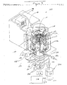
- process module 100 uses a transfer arm (not shown) to transfer a wafer ffom a vacuum wafer carrier 40 to processing chamber 106.
- Process module 100 can be formed from any suitable material, for example, stainless steel or aluminum.
- Process module 100 can be either connected to central transfer chamber or can be physically separated Kom other process modules with the wafer 48 being transported between modules using vacuum wafer carrier 40.
- Process module 40 is similar to those disclosed in U.S. Patent Application Serial No. 074,448, filed July 16, 1987 which is hereby incorporated by reference.
- Process chamber 106 where the actual processing is accomplished, is con tained within process module 100.
- Process chamber 106 has vertical walls 107 which can be made from any suitable material, for instance, quartz.
- the vertical walls 107 form a cylinder about the vertical axis of process chamber 106.
- the bottom 117 of process chamber 106 is also be made from any suitable material, for instance, quartz.
- Heated substrate 114 forms the upper boundary of process chamber 106 and can be formed from any suitable material, for example, stainless steel.
- vertical walls 107 are moved down for transfer and up for processing.
- Bellows 116 is attached to and moves vertical walls 107 up and down.
- the transfer arm (not shown) can transfer the wafer 48 from the carrier 40 through loadlock chamber 42 and into the process chamber 106 onto a plurality of fingers or pins 142.
- the up position vertical walls 107 contact substrate 114 or an adjacent portion of module 100.
- a seal (not shown) can be provided at the location where the vertical walls 107 come into contact with heated substrate 114 or the adjacent portion of process module 100.
- the fingers 120 move upward to place the wafer 48 into contact with the heated substrate 114.
- Process gas distributor ring 104 which is located in the upper part of the process chamber 106 and heated substrate 114.
- the process gas distributor ring 104 which is formed from any suitable material, for instance, quartz, can supply a gas mixture to the process chamber 106 from pipe 122.
- Process gas distributor ring 104 is arranged about the vertical axis of chamber 106. The gas exits from the process gas distributor ring 104 through a plurality of openings 112 in the bottom of the process gas distributor ring 104.
- Pipe 122 extends from the mass flow controller 126 into chamber 130 through chamber bottom 117 and along the vertical axis of process chamber 106.
- the pipe 122 has, for example, a slip or a bellows 128 to accommodate the vertical movement of chamber 106, including the chamber bottom 117.
- Gas distributor ring 104 fits into an open end 138 of pipe 122. Gas distributor ring 104 is arranged concentrically within process chamber 106. Below chamber bottom 117 there is located chamber 130 which is connected to pump 132 and valve 136. Thus, a generally downward flow through chambers 106 and 130 is provided. Pump 132 and valve 136 provide the desired vacuum within the chamber 106. Wafer temperature can be controlled through the adjustment of power supplied heater power controller (not shown) to heated substrate 114. Heater power controller could be connected to process computer 218.
- Processing module 100 allows the use of a vaporized liquid as source for the gas mixture being supplied to gas distributor ring 104.
- the gas mixture can be generated from suitable liquid source, for example, a silylating agent such as hexamethyldisilazane (HMDS) in gas generator 200.
- Gas generator 200 contains a chamber 201 for holding the liquid and a heater 204 for vaporizing the liquid.
- the power supplied to heater 204 is supplied through controller 214.
- the power to the heaters 204 is controlled using a temperature sensor 216 (for example, a thermocouple) which senses the temperature in the chamber 201 and provides a signal corresponding to controller 214.
- the temperature setpoint for the controller is set by the process computer 218 which is connected to the controller 214.
- Process gas mixture flow rate and pressure is controlled by a series of gas supplies, mass flow controllers and a pressure sensor through the process computer 218.
- the gas mixture supplied to gas distributor ring 104 flows from the top of chamber 201 through mass flow controller 126 and then through pipe 122.
- Mass flow controller 126 receives signals from process computer 218.
- Process chamber 106 effluent is passed through exhaust line 138 through control valve 156 which also receives signals from process com puter 218.
- process pressure is detected using pressure sensor 154, for instance a 10K manometer, which is in fluid communication with process chamber 106 and provides a signal corresponding to process pressure to process computer 218.
- Process pressure sensed by pressure sensor 154 is controlled through adjustment to both mass flow controller 126 and control valve 156 by process computer 218.
- Processing module 100 also includes a purging capability. Purging of gas generator 200 can also be accomplished during purging of processing module 100.
- the purge is accomplished using a suitable purge gas, for example nitrogen, from purge gas source 206 supplied to the process chamber 106 through pipe 122 and mass flow controller 152 which is controlled through process computer 218.
- Purging of gas generator 200 is accomplished using the same purge gas source 206 through mass flow controller 150 which is controlled by process computer 218 the effluent passing from chamber 201 through mass flow controller 126, and pipe 122.
- Process chamber 106 effluent is drawn through valves 132 by vacuum pump 136.
- Process module 100 which includes only one module and one vacuum load lock, but it can also be used in embodiments where a central handling chamber is combined with plural process modules 100 and one or more vacuum load lock chambers 42.
- wafer 48 is first transferred to process chamber 106.
- Vacuum wafer carrier 40 is placed in loadlock 42.
- Loadlock 42 is pumped to a vacuum and the door (not shown) to the vacuum wafer carrier 40 is opened.
- an isolation port not shown between loadlock 42 and process chamber 106 is opened.
- Bellows 116 is down and, with the opening of the isolation port, allows transfer to process chamber 106 of wafer 48.
- the actual transfer is accomplished using a transfer arm (not shown) which removes wafer 48 from the vacuum wafer carrier 40 and places it on fingers 120 in process chamber 106.
- the transfer arm is retracted from the process chamber 106 and the isolation port closes completing the transfer evolution.
- the wafer 48 is placed in the processing position, i.e. in contact with the substrate 114 by the upward motion of bellows 116 which also closes process chamber 106.
- Heaters 140 are energized and the temperature as sensed by temperature sensor 216 of the gas generator 200 is raised to the setpoint, as determined by computer 218 and set by controller 214 and maintained there using heaters 140. Wafer temperature is established using heated substrate 114.
- the process gas mixture flow to process chamber 106 is initiated through mass flow controller 126 and the pressure in process chamber 106 is maintained, for example at 760 torr, using a control valve in conjunction with mass flow controller 156 which are both controlled by the process computer 218 using pressure sensor 154.
- the desired gas mixture is then supplied via pipe 122 to process gas distributor ring 104 and to the face of the wafer 48.
- process gas flow is stopped, and all the heater power is shut off.
- a suitable purge gas such as nitrogen, is applied to process chamber 106 from purge gas source 206 through mass flow controller 152.
- mass flow controller 152 When the purge is complete and the purge gas flow is stopped by mass flow controller 152, the bellows 116 moves downward thereby opening the process chamber 106 as described above, and allowing the transfer arm to enter the process chamber 106 and retrieve wafer 48 as described above. The transfer arm then returns the wafer 48 to the vacuum wafer carrier 40 in chamber 42 as described above.
- Wafers could be provided to loadlock 42 at atmospheric or other pressures.
- a change ( P) of 200 torr increases the silylation rate from unacceptably low (0.0 micron linewidth or complete under silylation) to unacceptably high (1.2 micron linewidth or 20over silylation). From a time perspective it is clear that for any pressure over 300 torr, correct silylation time must be considerably less than 1 minute. Such a short time period also would be hard to control. A small change in silylation time would lead to a relatively large change in resulting linewidth (extent of silylation). A 160° C silylation temperature, on the other hand, results in a considerably more easily controllable process as indicated by the slope of this approximated curve in Figure 4.
- Figure 5 depicts the result of measurements of the photosensitive resist layer thickness in exposed regions of the resist after plasma oxygen etch using the same etch process parameters and a one minute silylation time using wafer having the same photosensitive resist material and using the same silylating agent (HMDS) as used in Figure 4.
- the resist thickness before processing was 1.5 microns for all wafers. Therefore, it is desired in the best case that as close as practical to 1.5 microns of resist material remains after etching.
- the desired thickness is graphically represented by dotted line 51.
- wafers made of other materials such as germanium, etc. can also be etched.
- the wafers can be comprised of many different configurations, for example, a single piece of crystals material or small crystals located on a larger substrate.
- wafers such as 48 are disclosed herein, other types of flat workpieces could be used with the techniques disclosed herein.
- the result of processing the wafer 48 can be electronic devices, for example, integrated circuits or discreet semiconductor devices.
- the wafers are divided into devices.
- the circuits and devices are enclosed into packages, for example, as shown in U. S. Patent 4,465,898 issued to Orcutt, et al., on August 14, 1984 and 3,439,238 issued to Birchler, et al. on April 15, 1969, which are incorporated hereinto by reference. These packages are then utilized in the construction of printed circuit boards.
- the present invention advantageously provides better control of the photolithographic development process.
- This invention allows a faster silylation rate and thus can increase the manufacturing throughput.
- This invention allows the performance of several processing steps while maintaining a wafer under a vacuum and in a face down configuration in the same or another similar chamber.
Landscapes
- Chemical & Material Sciences (AREA)
- Chemical Kinetics & Catalysis (AREA)
- Inorganic Chemistry (AREA)
- Organic Chemistry (AREA)
- Physics & Mathematics (AREA)
- General Physics & Mathematics (AREA)
- Photosensitive Polymer And Photoresist Processing (AREA)
- Exposure Of Semiconductors, Excluding Electron Or Ion Beam Exposure (AREA)
- Drying Of Semiconductors (AREA)
Applications Claiming Priority (4)
| Application Number | Priority Date | Filing Date | Title |
|---|---|---|---|
| US24587888A | 1988-09-16 | 1988-09-16 | |
| US26520588A | 1988-10-31 | 1988-10-31 | |
| US245878 | 1994-05-19 | ||
| US265205 | 1999-03-10 |
Publications (3)
| Publication Number | Publication Date |
|---|---|
| EP0359221A2 true EP0359221A2 (de) | 1990-03-21 |
| EP0359221A3 EP0359221A3 (de) | 1992-08-19 |
| EP0359221B1 EP0359221B1 (de) | 1996-05-15 |
Family
ID=26937529
Family Applications (1)
| Application Number | Title | Priority Date | Filing Date |
|---|---|---|---|
| EP19890116936 Expired - Lifetime EP0359221B1 (de) | 1988-09-16 | 1989-09-13 | Hochdruck-Photolack Siliconisierungsverfahren und Vorrichtung |
Country Status (3)
| Country | Link |
|---|---|
| EP (1) | EP0359221B1 (de) |
| JP (1) | JP3111071B2 (de) |
| DE (1) | DE68926480T2 (de) |
Cited By (2)
| Publication number | Priority date | Publication date | Assignee | Title |
|---|---|---|---|---|
| DE4040117A1 (de) * | 1990-12-13 | 1992-06-17 | Fotochem Werke Gmbh | Trockenentwickelbares negativresistsystem und dessen verarbeitungsprozess fuer die elektronenstrahl- und roentgenstrahllithographie |
| EP1228528A4 (de) * | 1999-09-10 | 2009-10-28 | Oerlikon Usa Inc | Prozess und anordnung zur herstellung magnetischer pole |
Family Cites Families (5)
| Publication number | Priority date | Publication date | Assignee | Title |
|---|---|---|---|---|
| KR900001666B1 (ko) * | 1985-07-19 | 1990-03-17 | 후지쓰가부시끼가이샤 | 화합물 반도체의 에피택셜층 성장용의 화학적 유기 금속 기상 성장장치 |
| FR2590405B1 (fr) * | 1985-11-21 | 1988-02-05 | Pons Michel | Procede de gravure de materiaux organiques par plasma |
| CA1287594C (en) * | 1986-04-04 | 1991-08-13 | Miroslav Eror | Method and apparatus for handling and processing wafer like materials |
| EP0267233B1 (de) * | 1986-04-28 | 1993-01-07 | Varian Associates, Inc. | Modulare förder- und beabeitungsanlage für halbleiterwafer |
| US4768291A (en) * | 1987-03-12 | 1988-09-06 | Monarch Technologies Corporation | Apparatus for dry processing a semiconductor wafer |
-
1989
- 1989-09-13 EP EP19890116936 patent/EP0359221B1/de not_active Expired - Lifetime
- 1989-09-13 DE DE1989626480 patent/DE68926480T2/de not_active Expired - Fee Related
- 1989-09-14 JP JP01237407A patent/JP3111071B2/ja not_active Expired - Fee Related
Cited By (2)
| Publication number | Priority date | Publication date | Assignee | Title |
|---|---|---|---|---|
| DE4040117A1 (de) * | 1990-12-13 | 1992-06-17 | Fotochem Werke Gmbh | Trockenentwickelbares negativresistsystem und dessen verarbeitungsprozess fuer die elektronenstrahl- und roentgenstrahllithographie |
| EP1228528A4 (de) * | 1999-09-10 | 2009-10-28 | Oerlikon Usa Inc | Prozess und anordnung zur herstellung magnetischer pole |
Also Published As
| Publication number | Publication date |
|---|---|
| JPH02210446A (ja) | 1990-08-21 |
| JP3111071B2 (ja) | 2000-11-20 |
| EP0359221A3 (de) | 1992-08-19 |
| EP0359221B1 (de) | 1996-05-15 |
| DE68926480T2 (de) | 1996-10-02 |
| DE68926480D1 (de) | 1996-06-20 |
Similar Documents
| Publication | Publication Date | Title |
|---|---|---|
| US5094936A (en) | High pressure photoresist silylation process and apparatus | |
| US12278125B2 (en) | Integrated dry processes for patterning radiation photoresist patterning | |
| US4882008A (en) | Dry development of photoresist | |
| US6645702B1 (en) | Treat resist surface to prevent pattern collapse | |
| KR102680084B1 (ko) | 금속-함유 포토레지스트의 재작업 (rework) | |
| KR102883937B1 (ko) | 포토레지스트의 건식 배면 및 베벨 에지 세정 | |
| EP0909989A1 (de) | Photolithographisches Verarbeitungsverfahren und Vorrichtung | |
| JP4519186B2 (ja) | ウェーハトラック環境内のプラズマ処理チャンバを用いて半導体ウェーハを処理する方法及び装置 | |
| EP0136130A2 (de) | Verfahren zur Herstellung von Gegenständen mit Plasma-Entwicklung unter Verwendung einer aktiven Gasschicht | |
| EP0359221B1 (de) | Hochdruck-Photolack Siliconisierungsverfahren und Vorrichtung | |
| US12204253B2 (en) | In-situ lithography pattern enhancement with localized stress treatment tuning using heat zones | |
| EP0370486A2 (de) | Hochtemperatur-Reaktionsverfahren | |
| US20250068065A1 (en) | Enhanced euv underlayer effect with diffusion barrier layer | |
| JPH09312247A (ja) | パターン形成方法及びパターン形成装置 | |
| US5085729A (en) | Uniformity using stagnant silylation | |
| TWI907354B (zh) | 具有多個圖案化輻射吸收成分及/或垂直組成梯度的光阻 | |
| US20260022465A1 (en) | Systems for manufacturing semiconductor device and relevant methods | |
| Misium et al. | Surface imaging lithography at 248 nm | |
| JP2000049084A (ja) | 半導体製造装置 | |
| JPH0757998A (ja) | 重合体薄膜の製造方法 | |
| JPH05283333A (ja) | 反応処理装置 |
Legal Events
| Date | Code | Title | Description |
|---|---|---|---|
| PUAI | Public reference made under article 153(3) epc to a published international application that has entered the european phase |
Free format text: ORIGINAL CODE: 0009012 |
|
| AK | Designated contracting states |
Kind code of ref document: A2 Designated state(s): BE DE FR GB IT |
|
| PUAL | Search report despatched |
Free format text: ORIGINAL CODE: 0009013 |
|
| AK | Designated contracting states |
Kind code of ref document: A3 Designated state(s): BE DE FR GB IT |
|
| 17P | Request for examination filed |
Effective date: 19930108 |
|
| 17Q | First examination report despatched |
Effective date: 19950111 |
|
| GRAH | Despatch of communication of intention to grant a patent |
Free format text: ORIGINAL CODE: EPIDOS IGRA |
|
| GRAA | (expected) grant |
Free format text: ORIGINAL CODE: 0009210 |
|
| ITF | It: translation for a ep patent filed | ||
| AK | Designated contracting states |
Kind code of ref document: B1 Designated state(s): BE DE FR GB IT |
|
| PG25 | Lapsed in a contracting state [announced via postgrant information from national office to epo] |
Ref country code: BE Effective date: 19960515 |
|
| REF | Corresponds to: |
Ref document number: 68926480 Country of ref document: DE Date of ref document: 19960620 |
|
| ET | Fr: translation filed | ||
| PLBE | No opposition filed within time limit |
Free format text: ORIGINAL CODE: 0009261 |
|
| STAA | Information on the status of an ep patent application or granted ep patent |
Free format text: STATUS: NO OPPOSITION FILED WITHIN TIME LIMIT |
|
| 26N | No opposition filed | ||
| REG | Reference to a national code |
Ref country code: GB Ref legal event code: IF02 |
|
| PGFP | Annual fee paid to national office [announced via postgrant information from national office to epo] |
Ref country code: GB Payment date: 20060804 Year of fee payment: 18 |
|
| PGFP | Annual fee paid to national office [announced via postgrant information from national office to epo] |
Ref country code: FR Payment date: 20060906 Year of fee payment: 18 |
|
| PGFP | Annual fee paid to national office [announced via postgrant information from national office to epo] |
Ref country code: DE Payment date: 20060929 Year of fee payment: 18 |
|
| PGFP | Annual fee paid to national office [announced via postgrant information from national office to epo] |
Ref country code: IT Payment date: 20060930 Year of fee payment: 18 |
|
| GBPC | Gb: european patent ceased through non-payment of renewal fee |
Effective date: 20070913 |
|
| PG25 | Lapsed in a contracting state [announced via postgrant information from national office to epo] |
Ref country code: DE Free format text: LAPSE BECAUSE OF NON-PAYMENT OF DUE FEES Effective date: 20080401 |
|
| REG | Reference to a national code |
Ref country code: FR Ref legal event code: ST Effective date: 20080531 |
|
| PG25 | Lapsed in a contracting state [announced via postgrant information from national office to epo] |
Ref country code: FR Free format text: LAPSE BECAUSE OF NON-PAYMENT OF DUE FEES Effective date: 20071001 |
|
| PG25 | Lapsed in a contracting state [announced via postgrant information from national office to epo] |
Ref country code: GB Free format text: LAPSE BECAUSE OF NON-PAYMENT OF DUE FEES Effective date: 20070913 |
|
| PG25 | Lapsed in a contracting state [announced via postgrant information from national office to epo] |
Ref country code: IT Free format text: LAPSE BECAUSE OF NON-PAYMENT OF DUE FEES Effective date: 20070913 |