EP0357980A2 - A memory cell with capacitance for single event upset protection - Google Patents
A memory cell with capacitance for single event upset protection Download PDFInfo
- Publication number
- EP0357980A2 EP0357980A2 EP89114650A EP89114650A EP0357980A2 EP 0357980 A2 EP0357980 A2 EP 0357980A2 EP 89114650 A EP89114650 A EP 89114650A EP 89114650 A EP89114650 A EP 89114650A EP 0357980 A2 EP0357980 A2 EP 0357980A2
- Authority
- EP
- European Patent Office
- Prior art keywords
- memory cell
- type semiconductor
- semiconductor material
- recited
- heavily doped
- Prior art date
- Legal status (The legal status is an assumption and is not a legal conclusion. Google has not performed a legal analysis and makes no representation as to the accuracy of the status listed.)
- Granted
Links
Images


Classifications
-
- G—PHYSICS
- G11—INFORMATION STORAGE
- G11C—STATIC STORES
- G11C5/00—Details of stores covered by group G11C11/00
- G11C5/005—Circuit means for protection against loss of information of semiconductor storage devices
-
- G—PHYSICS
- G11—INFORMATION STORAGE
- G11C—STATIC STORES
- G11C11/00—Digital stores characterised by the use of particular electric or magnetic storage elements; Storage elements therefor
- G11C11/21—Digital stores characterised by the use of particular electric or magnetic storage elements; Storage elements therefor using electric elements
- G11C11/34—Digital stores characterised by the use of particular electric or magnetic storage elements; Storage elements therefor using electric elements using semiconductor devices
- G11C11/40—Digital stores characterised by the use of particular electric or magnetic storage elements; Storage elements therefor using electric elements using semiconductor devices using transistors
- G11C11/41—Digital stores characterised by the use of particular electric or magnetic storage elements; Storage elements therefor using electric elements using semiconductor devices using transistors forming static cells with positive feedback, i.e. cells not needing refreshing or charge regeneration, e.g. bistable multivibrator or Schmitt trigger
- G11C11/412—Digital stores characterised by the use of particular electric or magnetic storage elements; Storage elements therefor using electric elements using semiconductor devices using transistors forming static cells with positive feedback, i.e. cells not needing refreshing or charge regeneration, e.g. bistable multivibrator or Schmitt trigger using field-effect transistors only
- G11C11/4125—Cells incorporating circuit means for protecting against loss of information
-
- H—ELECTRICITY
- H10—SEMICONDUCTOR DEVICES; ELECTRIC SOLID-STATE DEVICES NOT OTHERWISE PROVIDED FOR
- H10B—ELECTRONIC MEMORY DEVICES
- H10B10/00—Static random access memory [SRAM] devices
- H10B10/12—Static random access memory [SRAM] devices comprising a MOSFET load element
-
- Y—GENERAL TAGGING OF NEW TECHNOLOGICAL DEVELOPMENTS; GENERAL TAGGING OF CROSS-SECTIONAL TECHNOLOGIES SPANNING OVER SEVERAL SECTIONS OF THE IPC; TECHNICAL SUBJECTS COVERED BY FORMER USPC CROSS-REFERENCE ART COLLECTIONS [XRACs] AND DIGESTS
- Y10—TECHNICAL SUBJECTS COVERED BY FORMER USPC
- Y10S—TECHNICAL SUBJECTS COVERED BY FORMER USPC CROSS-REFERENCE ART COLLECTIONS [XRACs] AND DIGESTS
- Y10S257/00—Active solid-state devices, e.g. transistors, solid-state diodes
- Y10S257/903—FET configuration adapted for use as static memory cell
- Y10S257/904—FET configuration adapted for use as static memory cell with passive components,, e.g. polysilicon resistors
Definitions
- This invention is in the field of integrated circuits and is specifically directed to static random access memories.
- Static memory cells in certain environments in which radiation is present such as communication satellite orbital space are, or will likely be particularly susceptible to soft errors or single event upsets (SEUs).
- SEUs single event upsets
- E. G. Muller, M. S. Gussenhower, K. A. Lynch and D. H. Brenteger "DMSP Dosimetry Data: A Space Measurement and Mapping of Upset Causing Phenomena”. IEEE Trans. Nuclear Science NS-34, pp. 1251-1255 (1987) and H. T. Weaver, et al., “An SEU Tolerant Memory Cell Derived from Fundamental Studies of SEU Mechanisms in SRAM", IEEE Trans. Nuclear Science, NS-34, pp. 1281-1286 (1987).
- a soft error or single event upset is typically caused by electron-hole pairs created by, and along the path of, a single energetic particle as it passes through an integrated circuit, such as a memory. Should the energetic particle generate the critical charge in the critical volume of a memory cell, then the logic state of the memory is upset.
- This critical charge is the minimum amount of electrical charge required to change the logic state of the memory cell. The critical charge may also enter the memory through direct ionization from cosmic rays. See T. C. May and M. H. Woods, "Alpha Particle Induced Soft Errors in Dynamic Memories, IEEE Trans. Electronic Devices, ED-26, p. 2 (1979) and J. C. Pickel, J. T.
- CMOS RAM Cosmic Ray - Induced Error Rate Analysis IEEE Trans. on Nuclear Science, Vol. NS-28, pp. 3962-3967 (1981).
- the critical charge may result from alpha particles (helium nuclei).
- SEU SEU
- figure 1a illustrates a cross-sectional view of a CMOS inverter. When alpha particle p strikes bulk semiconductor material in p-channel MOS transistor Pch it generates electron-hole pairs as shown by the respective minus and plus marks.
- FIG 1b illustrates a schematic drawing of a conventional CMOS (complementary metal oxide semiconductor) static memory cell, typically used in a static random access memory (SRAM).
- Memory cell 2 is constructed according to well known methods of cross-coupled inverter realization and thus CMOS inverters are used in memory cell 2. (Note that the word metal used in the phrase metal oxide semiconductor is interpreted in semiconductor and related arts as also encompassing polycrystalline material).
- a first CMOS inverter 4 in memory cell 2 is made up of p-channel transistor 6 and n-channel transistor 8 having their source-to-drain paths connected in series between Vcc and ground, and having their gates tied together.
- the second CMOS inverter 5 in memory cell 2 is similarly constructed, with p-channel transistor 10 and n-channel transistor 12 having their source-to-drain paths connected in series between Vcc and ground and their gates also common.
- the cross-coupling is accomplished by the gates of transistors 6 and 8 being connected to the drains of transistors 10 and 12 (node S1 of figure 1b), and by the gates of transistors 10 and 12 being connected to the drains of transistors 6 and 8 (node S2 of figure 1b).
- N-channel pass transistor 14 has its source-to drain path connected between node S2 and a first bit line BL, and has its gate connected to word line WL.
- N-channel pass transistor 16 similarly has its source-to-drain path connected between node S1 and a second bit line BL_, and has its gate also connected to word line WL.
- Pass transistors 14, 16 when enabled, allow data to pass into and out of memory cell 2 from bit lines BL and BL_ respectively.
- Bit lines BL and BL_ carry data into and out of memory cell 2.
- Pass transistors 14, 16 are enabled by word line WL which is a function of the row address in an SRAM. The row address is decoded by a row decoder in the SRAM such that one out of n word lines is enabled, where n is the number of rows of memory cells in the memory which is a function of memory density and architecture.
- node S1 and S2 will necessarily be logical complements of one another, due to the cross-coupled nature of CMOS inverters 4,5 within memory cell 2.
- word line WL is energized by the row decoder (not shown), according to the row address received at address inputs to an address buffer (not shown) connected to the row decoder, pass transistors 14 and 16 will be turned on, coupling nodes S1 and S2 to bit lines BL_ and BL, respectively. Accordingly, when word line WL is high, the state of memory cell 2 can establish a differential voltage on BL and BL_. Alternatively, peripheral circuitry forcing a voltage on BL and BL_ can alter the state of memory cell 2.
- the sizes of the transistors shown in figure 1b are generally chosen such that when pass transistors 14 and 16 are turned on by word line WL; a differentially low voltage at bit line BL with respect to bit line BL_ can force node S2 to a logic low level; and a differentially low voltage at bit line BL_ with respect to bit line BL can force node S1 to a logic low level.
- the sizes of the transistors shown in figure 1 are also chosen such that when transistors 14 and 16 are on; a differentially high voltage at bit line BL with respect to bit line BL_ will not force node S2 high; nor will a differentially high voltage at bit line BL_ with respect to bit line BL force node S1 high. Therefore writing into memory cell 2 is accomplished by pulling the desired bit line and thus the desired side of cell 2 at either node S1 or node S2 low, which in turn due to feedback paths in cell 2, causes the opposite side of cell 2 to have a logic high state.
- One method for hardening a memory cell against SEU is by reducing the amount of charge generated by a given event. This is accomplished for example, by using a silicon film thinner than the collection depth in bulk material.
- a memory cell created on a thin film of silicon, such as in a SOI (silicon on insulator) device is less susceptible to SEU than one created on bulk semiconductor such as silicon because ionization charge along a path in an insulator is more likely to recombine than be collected compared to ionization charge created in a semiconductor.
- FIG. 1 Another way to reduce the susceptibility of a memory cell to upset is by increasing the critical charge of the cell.
- a hardening scheme against SEU in static memory cells based on increasing the critical charge required to produce SEU is illustrated in the schematic drawing of figure 2.
- resistors 18 and 20 are included in the cross-coupling lines of inverters 4 and 5 and they increase the RC time constant delay associated with the gate capacitances of transistors 6, 8, 10, and 12.
- the initial effect of an energetic particle strike in a critical volume is to change the voltage of one node of the memory cell, say node S1. Upset will occur if this change in voltage propagates through the cross coupling of inverters 4 and 5 before the initial voltage of node S1 is restored.
- the increased RC delay slows the feedback propagation through the cross coupling and allows more time for recovery of the initially affected node.
- this increase in RC propagation delay also slows the write cycle time of cell 2.
- the write cycle of an SRAM has typically been faster than the read cycle so that some slowing of the write cycle has been acceptable, since the read cycle time was the most critical.
- the speed of the write cycle of SEU hardened cells has become critical. Therefore, this resistive approach to SEU hardening is no longer desirable.
- FIG. 3 illustrates the same circuit schematic as figure 1b with the exception that capacitor 21 is connected across the drains of inverters S1 and S2.
- a memory cell including cross-coupled inverters and having a MOS capacitor with both n+ semiconductor material and p+ semiconductor material connections to the capacitor channel, thereby allowing a high capacitance to be maintained for positive and negative capacitor gate voltages.
- the MOS capacitor is connected across the cross-coupling of the inverters to increase single event upset hardness.
- dynamic memory (memory requiring refresh) can be substituted in place of the static memory and include the foregoing discussed MOS capacitor structure.
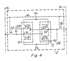
- FIG 4 A schematic drawing of an integrated circuit which embodies the invention is illustrated in figure 4. Note that for optimum SEU hardness that this circuit is built on an insulator body (although it can be built on bulk semiconductor material) and therefore can be classified as an SOI device.
- Figure 4 illustrates the same circuit schematic shown in figure 3 with the exception that capacitor 22 has been drawn in two parts: capacitor 24 and capacitor 26. Capacitor 24 is connected to and between the common drain and the the common gate of transistors 6 and 8; and capacitor 26 is connected to and between the common gate and the common drain of transistors 10 and 12. Additionally, Vss has been substituted for the ground node in figure 3 to indicate that a voltage in addition to circuit ground can be held by that node. Likewise as with the circuit shown in figure 3, this circuit does not negatively affect the write cycle time by a significant amount.
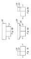
- capacitors 24 and 26 are shown in figures 5a, 5b, 5c, and 5d which illustrate front, top, left side and ride side views respectively.
- Each capacitor 24, 26 of figure 4, as shown by figures 5a through 5d comprises capacitor gate 28 (preferably made of polycrystalline silicon), capacitor gate oxide 34 lying over lightly doped p-type region p-, heavily doped n-type source/drain region n+, and heavily doped p-type source/drain region p+ adjacent to the n+ source/drain region.
- the capacitors shown in figure 4 are MOS capacitors which can be formed by extension of a polysilicon gate over regions of a drain area.
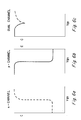
- Figures 6a through 6c are graphs showing the variation in capacitance with the variation in gate to source voltage Vgs between gate 28 and region n+ and alternatively region p+ as shown in the drawings of figures 5a through 5d.
- the capacitance variation represented in Figures 6a through 6c is primarily due to the formation of an accumulation layer or an inversion layer in the channel region of the MOS capacitor.
- the capacitance on the accumulation (n-type) layer side of the MOS capacitor is higher for larger positive values of Vgs (capacitor gate to source voltage) than for smaller values.
- figure 6b shows that the capacitance on inversion 5 (p-type) layer side is higher for larger negative values of Vgs than for smaller negative values.
- Figure 6c demonstrates that due to the dual channel contacted by the p+ and n+ regions (illustrated in figures 5a through 5d) of capacitors 24, and 26, their capacitance is maintained at a relatively high value for both negative and positive gate voltages. Since the gate to source voltage will be either substantially positive or substantially negative for the two stable states of the memory cell, the dual channel contact gives a consistently large capacitance for a given area.
- Figure 7a illustrates the superposition of a plurality of portions of photolithographic masks so as to show the physical layout of memory cell 2 of figure 4 as well as the relative positions of elements within memory cell 2.
- the position of word line WL (shown at labeled vertical lines) indicates it serves as the gate of transistors 14 and 16.
- One drain/source d/s region of transistor 14 and 16 is connected at via contact region 42 by a metal or polycrystalline semiconductor material (i.e. silicon) to areas for respective bit lines BL and BL_.
- Diagonal lines represent the positions for p-type material regions.
- Gate shown as triangular cross hatched lines
- drain and source regions for transistors 6, 8, 10, and 12 in Figure 4 are labeled g, d and s respectively.
- the common drain of transistors 6 and 8 are connected at region 44 by metal or polycrystalline semiconductor to region 46 which is connected to the common gate of transistors 10 and 12.
- the common drain of transistors 10 and 12 5 are connected at region 44 to region 46 which is connected to the common gate of transistors 6 and 8.
- Positions for contacts to Vcc and Vss are also indicated.
- Positions for capacitors 24 and 26 are indicated in the checkered regions with the location of capacitor n+ regions labeled n+ and capacitor p+ regions labeled 10 p+.
- Positions 40 are indicated for p+ regions which help eliminate leakage due to gate sidewall channels.
- Figure 7b illustrates a plurality of portions of photolithographic masks which help form the memory cell in moat region m.
- the common gate g (see cross-hatched area) of transistors 6 and 8 is shown extended to form capacitor 24 which comprises the common drain of inverter 4 and common gate g of inverter 4.
- common gate g (see cross-hatched area) of transistors 10 and 12 are shown extended to form capacitor 26 which comprisises the common drain of inverter 5 and common gate g of inverter 5.
- FIG. 8a A brief overview of a possible fabrication process for making capacitors 24 and 26, omitting annealing steps and other sundry details which will be apparent, after reading the following description, to those skilled in the art, shall be described with reference to figures 8a through 8e which give three dimensional views of the capacitor structure during various stages of formation.
- a silicon 52 on insulator 54 i.e. silicon dioxide
- a mesa is etched as shown in figure 8b.
- a light acceptor e.g. boron
- an oxide layer 56 is grown.
- Polysilicon gate 58 is then deposited and patterned, followed by a heavy masked donor implant (see n+ region under implant indicating arrows) and then followed by a heavy masked acceptor implant (see p+ region under implant indicating arrows). Titanium is sputtered over the structure thus formed and sintered in a nitrogen ambient to form conductive titanium silicide overections between the n+ and p+ regions. The silicide over the n+ and p+ regions allow formation of a common node.
Abstract
Description
- This invention is in the field of integrated circuits and is specifically directed to static random access memories.
- This invention was made with Government support under contract number DNA 001-86-C-0090S-408 awarded by the Defense Nuclear agency. The Government has certain rights in this invention.
- Static memory cells in certain environments in which radiation is present such as communication satellite orbital space are, or will likely be particularly susceptible to soft errors or single event upsets (SEUs). See E. G. Muller, M. S. Gussenhower, K. A. Lynch and D. H. Brenteger, "DMSP Dosimetry Data: A Space Measurement and Mapping of Upset Causing Phenomena". IEEE Trans. Nuclear Science NS-34, pp. 1251-1255 (1987) and H. T. Weaver, et al., "An SEU Tolerant Memory Cell Derived from Fundamental Studies of SEU Mechanisms in SRAM", IEEE Trans. Nuclear Science, NS-34, pp. 1281-1286 (1987). A soft error or single event upset (SEU) is typically caused by electron-hole pairs created by, and along the path of, a single energetic particle as it passes through an integrated circuit, such as a memory. Should the energetic particle generate the critical charge in the critical volume of a memory cell, then the logic state of the memory is upset. This critical charge, by definition, is the minimum amount of electrical charge required to change the logic state of the memory cell. The critical charge may also enter the memory through direct ionization from cosmic rays. See T. C. May and M. H. Woods, "Alpha Particle Induced Soft Errors in Dynamic Memories, IEEE Trans. Electronic Devices, ED-26, p. 2 (1979) and J. C. Pickel, J. T. Blaudfood, Jr., "CMOS RAM Cosmic Ray - Induced Error Rate Analysis", IEEE Trans. on Nuclear Science, Vol. NS-28, pp. 3962-3967 (1981). Alternatively, the critical charge may result from alpha particles (helium nuclei). One example of SEU can be seen in figure 1a which illustrates a cross-sectional view of a CMOS inverter. When alpha particle p strikes bulk semiconductor material in p-channel MOS transistor Pch it generates electron-hole pairs as shown by the respective minus and plus marks. Assuming that n-channel transistor Nch is on and that p-channel transistor Pch is off, the holes which collect (see arrows toward drain D) at drain D can change the voltage at output OUT from a logic low to a logic high. The electrons as indicated by the minus signs will diffuse toward circuit supply voltage Vcc. A charge generating energetic particle hit on transistor Nch has the opposite effect with positive charges drifting towards ground and negative charges collecting at output OUT, thus possibly changing the logic state of the inverter.
- Further background follows with reference to figure 1b which illustrates a schematic drawing of a conventional CMOS (complementary metal oxide semiconductor) static memory cell, typically used in a static random access memory (SRAM).
Memory cell 2 is constructed according to well known methods of cross-coupled inverter realization and thus CMOS inverters are used inmemory cell 2. (Note that the word metal used in the phrase metal oxide semiconductor is interpreted in semiconductor and related arts as also encompassing polycrystalline material). A first CMOS inverter 4 inmemory cell 2 is made up of p-channel transistor 6 and n-channel transistor 8 having their source-to-drain paths connected in series between Vcc and ground, and having their gates tied together. The second CMOS inverter 5 inmemory cell 2 is similarly constructed, with p-channel transistor 10 and n-channel transistor 12 having their source-to-drain paths connected in series between Vcc and ground and their gates also common. The cross-coupling is accomplished by the gates oftransistors transistors 10 and 12 (node S1 of figure 1b), and by the gates oftransistors transistors 6 and 8 (node S2 of figure 1b). N-channel pass transistor 14 has its source-to drain path connected between node S2 and a first bit line BL, and has its gate connected to word line WL. N-channel pass transistor 16 similarly has its source-to-drain path connected between node S1 and a second bit line BL_, and has its gate also connected to word line WL. Passtransistors memory cell 2 from bit lines BL and BL_ respectively. Bit lines BL and BL_ carry data into and out ofmemory cell 2.Pass transistors - In operation, the voltages of node S1 and S2 will necessarily be logical complements of one another, due to the cross-coupled nature of
CMOS inverters 4,5 withinmemory cell 2. When word line WL is energized by the row decoder (not shown), according to the row address received at address inputs to an address buffer (not shown) connected to the row decoder,pass transistors memory cell 2 can establish a differential voltage on BL and BL_. Alternatively, peripheral circuitry forcing a voltage on BL and BL_ can alter the state ofmemory cell 2. The sizes of the transistors shown in figure 1b are generally chosen such that whenpass transistors transistors memory cell 2 is accomplished by pulling the desired bit line and thus the desired side ofcell 2 at either node S1 or node S2 low, which in turn due to feedback paths incell 2, causes the opposite side ofcell 2 to have a logic high state. - One method for hardening a memory cell against SEU is by reducing the amount of charge generated by a given event. This is accomplished for example, by using a silicon film thinner than the collection depth in bulk material. For instance, a memory cell created on a thin film of silicon, such as in a SOI (silicon on insulator) device is less susceptible to SEU than one created on bulk semiconductor such as silicon because ionization charge along a path in an insulator is more likely to recombine than be collected compared to ionization charge created in a semiconductor.
- Another way to reduce the susceptibility of a memory cell to upset is by increasing the critical charge of the cell. A hardening scheme against SEU in static memory cells based on increasing the critical charge required to produce SEU is illustrated in the schematic drawing of figure 2. As shown,
resistors 18 and 20 are included in the cross-coupling lines ofinverters 4 and 5 and they increase the RC time constant delay associated with the gate capacitances oftransistors inverters 4 and 5 before the initial voltage of node S1 is restored. The increased RC delay slows the feedback propagation through the cross coupling and allows more time for recovery of the initially affected node. However, this increase in RC propagation delay also slows the write cycle time ofcell 2. The write cycle of an SRAM has typically been faster than the read cycle so that some slowing of the write cycle has been acceptable, since the read cycle time was the most critical. However, with scaling of memory cells to small geometries, the speed of the write cycle of SEU hardened cells has become critical. Therefore, this resistive approach to SEU hardening is no longer desirable. - Another hardening scheme against SEU based on increasing the critical charge is to increase the capacitance on the inverter drains, thus decreasing the voltage change on the node for a given amount of collected charge. The effectiveness of the capacitance in increasing the critical charge for SEU is increased by having the capacitance between the drains of the two inverters, which, with the cross coupling, is the same as between the gate and drain of the same inverter, as shown in figure 3. Figure 3 illustrates the same circuit schematic as figure 1b with the exception that capacitor 21 is connected across the drains of inverters S1 and S2. By having the capacitance between the gate and drain of the inverter, the effect of the capacitance is increased by the Miller capacitance. Also, with the capacitance from gate to drain, a change in the drain voltage induces a change in the gate voltage such that the restoring current is increased. Increased capacitance on the gate will also increase the RC delay in the feed back path, thus increasing resistance to SEU and also slowing the write; however, so long as the resistance is small, this effect will be minimal.
- It is an object of the invention to provide a new and improved memory cell.
- It is another object of the invention to provide a new and improved memory cell for use in a static random access memory.
- It is still another object of the invention to provide a new and improved memory cell having increase hardness against single event upset.
- It is yet still another object of the invention to provide a compact capacitor in a memory cell for high density memories.
- It is a further object of the invention to provide a compact capacitor in a memory cell which maintains a relatively high amount of capacitance for all capacitor gate voltages.
- The foregoing objects of the invention are accomplished by a memory cell including cross-coupled inverters and having a MOS capacitor with both n+ semiconductor material and p+ semiconductor material connections to the capacitor channel, thereby allowing a high capacitance to be maintained for positive and negative capacitor gate voltages. The MOS capacitor is connected across the cross-coupling of the inverters to increase single event upset hardness.
- Alternatively, dynamic memory (memory requiring refresh) can be substituted in place of the static memory and include the foregoing discussed MOS capacitor structure.
-
- Figure 1a is a cross-sectional view of a CMOS inverter.
- Figure 1b is a schematic drawing of a conventional CMOS memory cell typically used in an SRAM.
- Figure 2 is a schematic drawing of a prior art SEU hardening scheme based on increasing critical charge.
- Figure 3 is a schematic drawing of a SEU hardening scheme using capacitance in the inverter cross coupling.
- Figure 4 is a schematic drawing of the SEU hardening scheme which embodies the invention.
- Figures 5a through 5d are front, top, left side and right side views respectively of the invention's capacitor structure.
- Figures 6a through 6c graphs showing variation in capacitance with variation in gate to source voltage.
- Figures 7a and 7b illustrate the superposition of a plurality of photolithographic masks showing the physical layout of the memory cell.
- Figures 8a through 8e are three dimensional views of the capacitor structure during various stages of formation.
- A schematic drawing of an integrated circuit which embodies the invention is illustrated in figure 4. Note that for optimum SEU hardness that this circuit is built on an insulator body (although it can be built on bulk semiconductor material) and therefore can be classified as an SOI device. Figure 4 illustrates the same circuit schematic shown in figure 3 with the exception that capacitor 22 has been drawn in two parts:
capacitor 24 andcapacitor 26.Capacitor 24 is connected to and between the common drain and the the common gate oftransistors capacitor 26 is connected to and between the common gate and the common drain oftransistors - The structure of
capacitors capacitor capacitor gate oxide 34 lying over lightly doped p-type region p-, heavily doped n-type source/drain region n+, and heavily doped p-type source/drain region p+ adjacent to the n+ source/drain region. Thus, the capacitors shown in figure 4 are MOS capacitors which can be formed by extension of a polysilicon gate over regions of a drain area. This requires no additional contact and, depending on the layout of a cell without the capacitor, can add some capacitance without any increase in cell size. For example, in an 18 micrometer by 24 micrometer cell with size determined by requirements of the metal levels; a capacitor of area of approximately 29.8 square micrometers was added without increase in cell size and without modification of the fabrication process. Additional capacitance area can be provided with increased cell area, with the increase in capacitance area approaching the increase in cell area. - In operation (with reference to figures 5a through 5d), when a positive voltage is placed on
gate 28, a capacitance develops by a strong inversion layer forming a n-type channel undergate 28 in to which electrons from region n+ diffuse. Likewise, when a negative voltage is placed on gate 28 a capacitance develops by an accumulation of holes forming a p-type channel into which holes from region p+ diffuse. This structure also solves the previously discussed problem of maintaining a capacitance level for sufficient SEU hardening. - Figures 6a through 6c are graphs showing the variation in capacitance with the variation in gate to source voltage Vgs between
gate 28 and region n+ and alternatively region p+ as shown in the drawings of figures 5a through 5d. The capacitance variation represented in Figures 6a through 6c is primarily due to the formation of an accumulation layer or an inversion layer in the channel region of the MOS capacitor. Thus, as illustrated by Figure 6a, the capacitance on the accumulation (n-type) layer side of the MOS capacitor is higher for larger positive values of Vgs (capacitor gate to source voltage) than for smaller values. Similarly, figure 6b shows that the capacitance on inversion 5 (p-type) layer side is higher for larger negative values of Vgs than for smaller negative values. Figure 6c demonstrates that due to the dual channel contacted by the p+ and n+ regions (illustrated in figures 5a through 5d) ofcapacitors - Figure 7a illustrates the superposition of a plurality of portions of photolithographic masks so as to show the physical layout of
memory cell 2 of figure 4 as well as the relative positions of elements withinmemory cell 2. The position of word line WL (shown at labeled vertical lines) indicates it serves as the gate oftransistors transistor contact region 42 by a metal or polycrystalline semiconductor material (i.e. silicon) to areas for respective bit lines BL and BL_. Diagonal lines represent the positions for p-type material regions. Gate (shown as triangular cross hatched lines), drain and source regions fortransistors transistors region 44 by metal or polycrystalline semiconductor toregion 46 which is connected to the common gate oftransistors transistors region 44 toregion 46 which is connected to the common gate oftransistors capacitors Positions 40 are indicated for p+ regions which help eliminate leakage due to gate sidewall channels. - Figure 7b illustrates a plurality of portions of photolithographic masks which help form the memory cell in moat region m. Here the common gate g (see cross-hatched area) of
transistors capacitor 24 which comprises the common drain of inverter 4 and common gate g of inverter 4. Likewise, common gate g (see cross-hatched area) oftransistors capacitor 26 which comprisises the common drain ofinverter 5 and common gate g ofinverter 5. A brief overview of a possible fabrication process for makingcapacitors - Although the invention has been described in detail herein with reference to its preferred embodiment and certain described alternatives, it is to be understood that this description is by way of example only, and is not to be construed in a limiting sense. It is to be further understood that numerous changes in the details of the embodiments of the invention, and additional embodiments of the invention, will be apparent to, and may be made by, persons of ordinary skill in the art having reference to this description. For example, n-type semiconductor regions may be substituted consistently throughout with p-type semiconductor regions and vice verse. It is contemplated that all such changes and additional embodiments are within the spirit and true scope of the invention as claimed below.
Claims (18)
Applications Claiming Priority (2)
| Application Number | Priority Date | Filing Date | Title |
|---|---|---|---|
| US07/241,516 US5204990A (en) | 1988-09-07 | 1988-09-07 | Memory cell with capacitance for single event upset protection |
| US241516 | 1988-09-07 |
Publications (3)
| Publication Number | Publication Date |
|---|---|
| EP0357980A2 true EP0357980A2 (en) | 1990-03-14 |
| EP0357980A3 EP0357980A3 (en) | 1991-01-16 |
| EP0357980B1 EP0357980B1 (en) | 1995-01-11 |
Family
ID=22911002
Family Applications (1)
| Application Number | Title | Priority Date | Filing Date |
|---|---|---|---|
| EP89114650A Expired - Lifetime EP0357980B1 (en) | 1988-09-07 | 1989-08-08 | A memory cell with capacitance for single event upset protection |
Country Status (4)
| Country | Link |
|---|---|
| US (2) | US5204990A (en) |
| EP (1) | EP0357980B1 (en) |
| JP (1) | JP2915011B2 (en) |
| DE (1) | DE68920515T2 (en) |
Cited By (11)
| Publication number | Priority date | Publication date | Assignee | Title |
|---|---|---|---|---|
| US5359215A (en) * | 1990-11-26 | 1994-10-25 | Mitsubishi Denki Kabushiki Kaisha | Semiconductor memory cell for holding data with small power consumption |
| EP0633612A2 (en) * | 1993-07-09 | 1995-01-11 | Harris Corporation | Fast charging MOS capacitor structure for high magnitude voltage of either positive or negative polarity |
| WO1999063542A1 (en) * | 1998-06-05 | 1999-12-09 | Lockheed Martin Corporation | Radiation hardened six transistor random access memory and memory device |
| US6208554B1 (en) | 1999-05-28 | 2001-03-27 | Lockheed Martin Corporation | Single event upset (SEU) hardened static random access memory cell |
| US6275080B1 (en) | 1999-07-28 | 2001-08-14 | Bae Systems | Enhanced single event upset immune latch circuit |
| US6285580B1 (en) | 1999-05-28 | 2001-09-04 | Bae Systems Information | Method and apparatus for hardening a static random access memory cell from single event upsets |
| US6369630B1 (en) | 1999-11-24 | 2002-04-09 | Bae Systems Information And Electronic Systems Integration Inc. | Single-event upset hardened reconfigurable bi-stable CMOS latch |
| US6668342B2 (en) | 2000-04-28 | 2003-12-23 | Bae Systems Information And Electronic Systems Integration, Inc. | Apparatus for a radiation hardened clock splitter |
| EP1482514A2 (en) * | 2003-05-21 | 2004-12-01 | Altera Corporation | Programmable logic devices with stabilized configuration cells for reduced soft error rates |
| WO2006007566A1 (en) * | 2004-07-01 | 2006-01-19 | Altera Corporation | Integrated circuit structures for increasing resistance to single event upset |
| EP2922062A1 (en) * | 2014-03-21 | 2015-09-23 | STMicroelectronics (Rousset) SAS | Memory device including a SRAM memory plane and a non volatile memory plane, rugged against soft errors |
Families Citing this family (30)
| Publication number | Priority date | Publication date | Assignee | Title |
|---|---|---|---|---|
| US5204990A (en) * | 1988-09-07 | 1993-04-20 | Texas Instruments Incorporated | Memory cell with capacitance for single event upset protection |
| JPH0834059B2 (en) * | 1990-08-31 | 1996-03-29 | 三菱電機株式会社 | Semiconductor memory device |
| JP3359354B2 (en) * | 1991-06-24 | 2002-12-24 | テキサス インスツルメンツ インコーポレイテツド | Electronic latch with improved dynamic negative feedback |
| US5406513A (en) * | 1993-02-05 | 1995-04-11 | The University Of New Mexico | Mechanism for preventing radiation induced latch-up in CMOS integrated circuits |
| EP1045446A3 (en) * | 1994-09-30 | 2000-11-15 | Yozan Inc. | MOS invertor having a constricted channel width |
| US6163480A (en) * | 1997-12-29 | 2000-12-19 | Honeywell International Inc. | Memory with high integrity memory cells |
| US6252433B1 (en) | 1999-05-12 | 2001-06-26 | Southwest Research Institute | Single event upset immune comparator |
| US6696873B2 (en) | 1999-12-23 | 2004-02-24 | Intel Corporation | Single event upset hardened latch |
| US6377097B1 (en) | 2000-03-13 | 2002-04-23 | The United States Of America As Represented By The Administrator Of The National Aeronautics And Space Administration | Method and apparatus for reducing the vulnerability of latches to single event upsets |
| US6549443B1 (en) | 2001-05-16 | 2003-04-15 | Rockwell Collins, Inc. | Single event upset resistant semiconductor circuit element |
| US6573774B1 (en) * | 2002-03-25 | 2003-06-03 | Aeroflex Utmc Microelectronic Systems, Inc. | Error correcting latch |
| US7071749B2 (en) | 2002-03-25 | 2006-07-04 | Aeroflex Colorado Springs Inc. | Error correcting latch |
| AU2003223386A1 (en) * | 2002-03-27 | 2003-10-13 | The Regents Of The University Of California | Low-power high-performance memory cell and related methods |
| US7486541B2 (en) * | 2003-06-13 | 2009-02-03 | Taiwan Semiconductor Manufacturing Company, Ltd. | Resistive cell structure for reducing soft error rate |
| US6992916B2 (en) * | 2003-06-13 | 2006-01-31 | Taiwan Semiconductor Manufacturing Co., Ltd. | SRAM cell design with high resistor CMOS gate structure for soft error rate improvement |
| US7110281B1 (en) * | 2004-06-08 | 2006-09-19 | Xilinx, Inc. | Memory cells utilizing metal-to-metal capacitors to reduce susceptibility to single event upsets |
| US20060187700A1 (en) * | 2005-02-08 | 2006-08-24 | Iota Technology, Inc. | Single event effect (SEE) tolerant circuit design strategy for SOI type technology |
| US7372720B1 (en) | 2005-02-16 | 2008-05-13 | Altera Corporation | Methods and apparatus for decreasing soft errors and cell leakage in integrated circuit structures |
| US7545007B2 (en) * | 2005-08-08 | 2009-06-09 | International Business Machines Corporation | MOS varactor with segmented gate doping |
| US7397691B2 (en) | 2006-04-24 | 2008-07-08 | International Business Machines Corporation | Static random access memory cell with improved stability |
| US7397692B1 (en) * | 2006-12-19 | 2008-07-08 | International Business Machines Corporation | High performance single event upset hardened SRAM cell |
| US7468904B2 (en) * | 2007-02-23 | 2008-12-23 | Bae Systems Information And Electronic Systems Integration Inc. | Apparatus for hardening a static random access memory cell from single event upsets |
| US20090001481A1 (en) * | 2007-06-26 | 2009-01-01 | Ethan Harrison Cannon | Digital circuits having additional capacitors for additional stability |
| US7684232B1 (en) | 2007-09-11 | 2010-03-23 | Xilinx, Inc. | Memory cell for storing a data bit value despite atomic radiation |
| US7961501B1 (en) | 2008-07-10 | 2011-06-14 | Ryan Technologies, LLC | Radiation sensors and single-event-effects suppression devices |
| US8067803B2 (en) | 2008-10-16 | 2011-11-29 | Micron Technology, Inc. | Memory devices, transistor devices and related methods |
| US8824226B2 (en) * | 2009-04-02 | 2014-09-02 | Taiwan Semiconductor Manufacturing Company, Ltd. | Providing capacitors to improve radiation hardening in memory elements |
| JP5068296B2 (en) * | 2009-09-25 | 2012-11-07 | ルネサスエレクトロニクス株式会社 | Manufacturing method of semiconductor memory device |
| FR3055463A1 (en) * | 2016-08-31 | 2018-03-02 | St Microelectronics Crolles 2 Sas | CURED MEMORIZATION ELEMENT |
| CN112395823B (en) * | 2020-11-17 | 2022-08-16 | 湘潭大学 | Method for reinforcing standard unit against single event effect |
Citations (1)
| Publication number | Priority date | Publication date | Assignee | Title |
|---|---|---|---|---|
| JPS61100958A (en) * | 1984-10-22 | 1986-05-19 | Nec Corp | Semiconductor memory integrated circuit device |
Family Cites Families (15)
| Publication number | Priority date | Publication date | Assignee | Title |
|---|---|---|---|---|
| US3440444A (en) * | 1965-12-30 | 1969-04-22 | Rca Corp | Driver-sense circuit arrangement |
| US4827448A (en) * | 1976-09-13 | 1989-05-02 | Texas Instruments Incorporated | Random access memory cell with implanted capacitor region |
| JPS5598852A (en) * | 1979-01-23 | 1980-07-28 | Nec Corp | Memory device |
| US4453175A (en) * | 1979-09-19 | 1984-06-05 | Tokyo Shibaura Denki Kabushiki Kaisha | MOS Static RAM layout with polysilicon resistors over FET gates |
| JPS5683073A (en) * | 1979-12-11 | 1981-07-07 | Toshiba Corp | Semiconductor device |
| JPS59142800A (en) * | 1983-02-04 | 1984-08-16 | Fujitsu Ltd | Semiconductor storage device |
| JPS6038864A (en) * | 1983-08-11 | 1985-02-28 | Nec Corp | Semiconductor memory cell |
| JPS60260146A (en) * | 1984-06-06 | 1985-12-23 | Toshiba Corp | Semiconductor memory unit and manufacture thereof |
| US4745454A (en) * | 1985-01-07 | 1988-05-17 | Advanced Micro Devices, Inc. | High capacity semiconductor capacitance device structure |
| JPS61208698A (en) * | 1985-03-12 | 1986-09-17 | Matsushita Electronics Corp | Semiconductor memory device |
| US4725981A (en) * | 1986-02-03 | 1988-02-16 | Motorola, Inc. | Random access memory cell resistant to inadvertant change of state due to charged particles |
| US4833644A (en) * | 1986-08-26 | 1989-05-23 | General Electric Company | Memory cell circuit having radiation hardness |
| US4912675A (en) * | 1988-09-07 | 1990-03-27 | Texas Instruments, Incorporated | Single event upset hardened memory cell |
| US5204990A (en) * | 1988-09-07 | 1993-04-20 | Texas Instruments Incorporated | Memory cell with capacitance for single event upset protection |
| EP0412514A1 (en) * | 1989-08-08 | 1991-02-13 | Nec Corporation | Capacitance device |
-
1988
- 1988-09-07 US US07/241,516 patent/US5204990A/en not_active Expired - Lifetime
-
1989
- 1989-08-08 DE DE68920515T patent/DE68920515T2/en not_active Expired - Fee Related
- 1989-08-08 EP EP89114650A patent/EP0357980B1/en not_active Expired - Lifetime
- 1989-08-24 JP JP1218453A patent/JP2915011B2/en not_active Expired - Fee Related
-
1995
- 1995-05-03 US US08/434,257 patent/US5917212A/en not_active Expired - Lifetime
Patent Citations (1)
| Publication number | Priority date | Publication date | Assignee | Title |
|---|---|---|---|---|
| JPS61100958A (en) * | 1984-10-22 | 1986-05-19 | Nec Corp | Semiconductor memory integrated circuit device |
Non-Patent Citations (2)
| Title |
|---|
| PATENT ABSTRACTS OF JAPAN, vol. 10, no. 279 (E-439)[2335], 20th September 1986; & JP-A-61 100 958 (NEC CORP.) 19-05-1986 * |
| PATENT ABSTRACTS OF JAPAN, vol. 11, no. 17 (E-471)[2464], 17th January 1987; & JP-A-47 80 751 (NEC CORP.) 21-08-1986 * |
Cited By (19)
| Publication number | Priority date | Publication date | Assignee | Title |
|---|---|---|---|---|
| US5359215A (en) * | 1990-11-26 | 1994-10-25 | Mitsubishi Denki Kabushiki Kaisha | Semiconductor memory cell for holding data with small power consumption |
| US5473178A (en) * | 1990-11-26 | 1995-12-05 | Mitsubishi Denki Kabushiki Kaisha | Semiconductor memory cell for holding data with small power consumption |
| EP0633612A2 (en) * | 1993-07-09 | 1995-01-11 | Harris Corporation | Fast charging MOS capacitor structure for high magnitude voltage of either positive or negative polarity |
| EP0633612A3 (en) * | 1993-07-09 | 1995-06-14 | Harris Corp | Fast charging MOS capacitor structure for high magnitude voltage of either positive or negative polarity. |
| WO1999063542A1 (en) * | 1998-06-05 | 1999-12-09 | Lockheed Martin Corporation | Radiation hardened six transistor random access memory and memory device |
| US6111780A (en) * | 1998-06-05 | 2000-08-29 | Lockheed Martin Corporation | Radiation hardened six transistor random access memory and memory device |
| US6285580B1 (en) | 1999-05-28 | 2001-09-04 | Bae Systems Information | Method and apparatus for hardening a static random access memory cell from single event upsets |
| US6208554B1 (en) | 1999-05-28 | 2001-03-27 | Lockheed Martin Corporation | Single event upset (SEU) hardened static random access memory cell |
| US6275080B1 (en) | 1999-07-28 | 2001-08-14 | Bae Systems | Enhanced single event upset immune latch circuit |
| US6369630B1 (en) | 1999-11-24 | 2002-04-09 | Bae Systems Information And Electronic Systems Integration Inc. | Single-event upset hardened reconfigurable bi-stable CMOS latch |
| US6668342B2 (en) | 2000-04-28 | 2003-12-23 | Bae Systems Information And Electronic Systems Integration, Inc. | Apparatus for a radiation hardened clock splitter |
| EP1482514A2 (en) * | 2003-05-21 | 2004-12-01 | Altera Corporation | Programmable logic devices with stabilized configuration cells for reduced soft error rates |
| EP1482514A3 (en) * | 2003-05-21 | 2005-03-30 | Altera Corporation | Programmable logic devices with stabilized configuration cells for reduced soft error rates |
| US6876572B2 (en) | 2003-05-21 | 2005-04-05 | Altera Corporation | Programmable logic devices with stabilized configuration cells for reduced soft error rates |
| WO2006007566A1 (en) * | 2004-07-01 | 2006-01-19 | Altera Corporation | Integrated circuit structures for increasing resistance to single event upset |
| EP2922062A1 (en) * | 2014-03-21 | 2015-09-23 | STMicroelectronics (Rousset) SAS | Memory device including a SRAM memory plane and a non volatile memory plane, rugged against soft errors |
| FR3018944A1 (en) * | 2014-03-21 | 2015-09-25 | St Microelectronics Rousset | MEMORY DEVICE ASSOCIATING A MEMORY PLAN OF THE SRAM TYPE AND A NON-VOLATILE TYPE MEMORY PLAN CURED AGAINST ACCIDENTAL TILT |
| US9728248B2 (en) | 2014-03-21 | 2017-08-08 | Stmicroelectronics (Rousset) Sas | Semiconductor structure and memory device including the structure |
| US10304524B2 (en) | 2014-03-21 | 2019-05-28 | Stmicroelectronics (Rousset) Sas | Semiconductor structure and memory device including the structure |
Also Published As
| Publication number | Publication date |
|---|---|
| EP0357980A3 (en) | 1991-01-16 |
| DE68920515T2 (en) | 1995-05-18 |
| EP0357980B1 (en) | 1995-01-11 |
| JP2915011B2 (en) | 1999-07-05 |
| US5917212A (en) | 1999-06-29 |
| DE68920515D1 (en) | 1995-02-23 |
| US5204990A (en) | 1993-04-20 |
| JPH02181966A (en) | 1990-07-16 |
Similar Documents
| Publication | Publication Date | Title |
|---|---|---|
| US5204990A (en) | Memory cell with capacitance for single event upset protection | |
| US4912675A (en) | Single event upset hardened memory cell | |
| US4956814A (en) | Memory cell with improved single event upset rate reduction circuitry | |
| US6111780A (en) | Radiation hardened six transistor random access memory and memory device | |
| US5338963A (en) | Soft error immune CMOS static RAM cell | |
| US5046044A (en) | SEU hardened memory cell | |
| US7313012B2 (en) | Back-gate controlled asymmetrical memory cell and memory using the cell | |
| US4914629A (en) | Memory cell including single event upset rate reduction circuitry | |
| US7468904B2 (en) | Apparatus for hardening a static random access memory cell from single event upsets | |
| US6208554B1 (en) | Single event upset (SEU) hardened static random access memory cell | |
| JP2004200300A (en) | Sram cell and integrated memory circuit using it | |
| JP4065870B2 (en) | Dual port read SRAM cell with improved soft error immunity | |
| US5310694A (en) | Method for forming a transistor device with resistive coupling | |
| EP1672644A1 (en) | Single-event upset tolerant static random access memory cell | |
| US6285580B1 (en) | Method and apparatus for hardening a static random access memory cell from single event upsets | |
| US6259643B1 (en) | Single event upset (SEU) hardened static random access memory cell | |
| US6215694B1 (en) | Self-restoring single event upset (SEU) hardened multiport memory cell | |
| EP0357982B1 (en) | Memory cell with improved single event upset rate reduction circuitry | |
| US7269057B2 (en) | Method for connecting circuit elements within an integrated circuit for reducing single-event upsets | |
| EP0375226B1 (en) | An seu hardened memory cell | |
| Adams | Silicon On Insulator Memories: Design & Test Considerations |
Legal Events
| Date | Code | Title | Description |
|---|---|---|---|
| PUAI | Public reference made under article 153(3) epc to a published international application that has entered the european phase |
Free format text: ORIGINAL CODE: 0009012 |
|
| AK | Designated contracting states |
Kind code of ref document: A2 Designated state(s): DE FR GB IT NL |
|
| PUAL | Search report despatched |
Free format text: ORIGINAL CODE: 0009013 |
|
| AK | Designated contracting states |
Kind code of ref document: A3 Designated state(s): DE FR GB IT NL |
|
| 17P | Request for examination filed |
Effective date: 19910730 |
|
| 17Q | First examination report despatched |
Effective date: 19930215 |
|
| GRAA | (expected) grant |
Free format text: ORIGINAL CODE: 0009210 |
|
| ITF | It: translation for a ep patent filed |
Owner name: BARZANO' E ZANARDO ROMA S.P.A. |
|
| AK | Designated contracting states |
Kind code of ref document: B1 Designated state(s): DE FR GB IT NL |
|
| REF | Corresponds to: |
Ref document number: 68920515 Country of ref document: DE Date of ref document: 19950223 |
|
| ET | Fr: translation filed | ||
| PLBE | No opposition filed within time limit |
Free format text: ORIGINAL CODE: 0009261 |
|
| STAA | Information on the status of an ep patent application or granted ep patent |
Free format text: STATUS: NO OPPOSITION FILED WITHIN TIME LIMIT |
|
| 26N | No opposition filed | ||
| REG | Reference to a national code |
Ref country code: GB Ref legal event code: IF02 |
|
| PGFP | Annual fee paid to national office [announced via postgrant information from national office to epo] |
Ref country code: GB Payment date: 20060706 Year of fee payment: 18 |
|
| PGFP | Annual fee paid to national office [announced via postgrant information from national office to epo] |
Ref country code: NL Payment date: 20060710 Year of fee payment: 18 |
|
| PGFP | Annual fee paid to national office [announced via postgrant information from national office to epo] |
Ref country code: FR Payment date: 20060803 Year of fee payment: 18 |
|
| PGFP | Annual fee paid to national office [announced via postgrant information from national office to epo] |
Ref country code: IT Payment date: 20060831 Year of fee payment: 18 Ref country code: DE Payment date: 20060831 Year of fee payment: 18 |
|
| GBPC | Gb: european patent ceased through non-payment of renewal fee |
Effective date: 20070808 |
|
| PG25 | Lapsed in a contracting state [announced via postgrant information from national office to epo] |
Ref country code: NL Free format text: LAPSE BECAUSE OF NON-PAYMENT OF DUE FEES Effective date: 20080301 |
|
| NLV4 | Nl: lapsed or anulled due to non-payment of the annual fee |
Effective date: 20080301 |
|
| REG | Reference to a national code |
Ref country code: FR Ref legal event code: ST Effective date: 20080430 |
|
| PG25 | Lapsed in a contracting state [announced via postgrant information from national office to epo] |
Ref country code: DE Free format text: LAPSE BECAUSE OF NON-PAYMENT OF DUE FEES Effective date: 20080301 |
|
| PG25 | Lapsed in a contracting state [announced via postgrant information from national office to epo] |
Ref country code: FR Free format text: LAPSE BECAUSE OF NON-PAYMENT OF DUE FEES Effective date: 20070831 |
|
| PG25 | Lapsed in a contracting state [announced via postgrant information from national office to epo] |
Ref country code: GB Free format text: LAPSE BECAUSE OF NON-PAYMENT OF DUE FEES Effective date: 20070808 |
|
| PG25 | Lapsed in a contracting state [announced via postgrant information from national office to epo] |
Ref country code: IT Free format text: LAPSE BECAUSE OF NON-PAYMENT OF DUE FEES Effective date: 20070808 |