EP0351983B1 - Geräte mit programmierbarer Logik mit Ersatzschaltungen zum Ersetzen defekter Schaltungen - Google Patents
Geräte mit programmierbarer Logik mit Ersatzschaltungen zum Ersetzen defekter Schaltungen Download PDFInfo
- Publication number
- EP0351983B1 EP0351983B1 EP89306839A EP89306839A EP0351983B1 EP 0351983 B1 EP0351983 B1 EP 0351983B1 EP 89306839 A EP89306839 A EP 89306839A EP 89306839 A EP89306839 A EP 89306839A EP 0351983 B1 EP0351983 B1 EP 0351983B1
- Authority
- EP
- European Patent Office
- Prior art keywords
- conductors
- regular
- spare
- conductor
- signals
- Prior art date
- Legal status (The legal status is an assumption and is not a legal conclusion. Google has not performed a legal analysis and makes no representation as to the accuracy of the status listed.)
- Expired - Lifetime
Links
Images


Classifications
-
- H—ELECTRICITY
- H03—ELECTRONIC CIRCUITRY
- H03K—PULSE TECHNIQUE
- H03K19/00—Logic circuits, i.e. having at least two inputs acting on one output; Inverting circuits
- H03K19/02—Logic circuits, i.e. having at least two inputs acting on one output; Inverting circuits using specified components
- H03K19/173—Logic circuits, i.e. having at least two inputs acting on one output; Inverting circuits using specified components using elementary logic circuits as components
- H03K19/177—Logic circuits, i.e. having at least two inputs acting on one output; Inverting circuits using specified components using elementary logic circuits as components arranged in matrix form
- H03K19/17748—Structural details of configuration resources
-
- H—ELECTRICITY
- H03—ELECTRONIC CIRCUITRY
- H03K—PULSE TECHNIQUE
- H03K19/00—Logic circuits, i.e. having at least two inputs acting on one output; Inverting circuits
- H03K19/02—Logic circuits, i.e. having at least two inputs acting on one output; Inverting circuits using specified components
- H03K19/173—Logic circuits, i.e. having at least two inputs acting on one output; Inverting circuits using specified components using elementary logic circuits as components
- H03K19/177—Logic circuits, i.e. having at least two inputs acting on one output; Inverting circuits using specified components using elementary logic circuits as components arranged in matrix form
- H03K19/17736—Structural details of routing resources
-
- H—ELECTRICITY
- H03—ELECTRONIC CIRCUITRY
- H03K—PULSE TECHNIQUE
- H03K19/00—Logic circuits, i.e. having at least two inputs acting on one output; Inverting circuits
- H03K19/02—Logic circuits, i.e. having at least two inputs acting on one output; Inverting circuits using specified components
- H03K19/173—Logic circuits, i.e. having at least two inputs acting on one output; Inverting circuits using specified components using elementary logic circuits as components
- H03K19/177—Logic circuits, i.e. having at least two inputs acting on one output; Inverting circuits using specified components using elementary logic circuits as components arranged in matrix form
- H03K19/17748—Structural details of configuration resources
- H03K19/17764—Structural details of configuration resources for reliability
Definitions
- This invention relates to programmable logic integrated circuits, and more particularly to programmable logic integrated circuits including spare circuits for use in replacing other possibly defectively manufactured circuits on the same chip.
- PLDs programmable logic integrated circuits or devices
- PLDs programmable logic devices
- spare circuits which can be programmably switched into the architecture of the device to replace any normal circuit which is found to be unusable (e.g., as a result of defective manufacture of the device).
- PLDs programmable logic devices
- This replacement of any defective or bad circuit with a spare circuit is done by "preprogramming" the chip in such a way that the ultimate user of the chip is unaware that the chip has been preprogrammed. This means that after such preprogramming and therefore during all phases of operation of the chip by the ultimate user, the chip automatically reroutes signals throughout the chip to avoid any defective circuit or circuits and to rely on spare circuits instead.
- FIGS. 1a and 1b are a schematic block diagram.
- FIGS. 2a and 2b are simplified wiring diagrams useful in explaining the operation of portions of FIG. 1.
- FIGS. 3a-3c (sometimes referred to collectively as FIG. 3) are simplified wiring diagrams useful in explaining the operation of portions of FIG. 4.
- FIGS. 4a and 4b are a schematic block diagram of an illustrative embodiment of the invention.
- FIGS. 5-7 are schematic diagrams of circuits which can be used to implement portions of the embodiment shown in FIG. 1.
- FIG. 8 is a schematic diagram of circuits which can be used to implement portions of the embodiments of FIGS. 1 and 4.
- PLDs vary greatly in size and architecture.
- the embodiments shown and described herein are merely illustrative of PLD architectures in which the invention can be employed.
- the invention is equally applicable to PLDs having many other architectures, including those which do not have some of the features of the depicted embodiments and those which have features additional to those of the depicted embodiments.
- FIG. 1 shows one device to which the subject matter of the present invention can be added or implemented in the context of the PLD shown in FIGS. 3-5 of application Serial No. 190,663.
- FIG. 1 shows one device to which the subject matter of the present invention can be added or implemented in the context of the PLD shown in FIGS. 3-5 of application Serial No. 190,663.
- the PLD shown in FIGS. 3-5 of application Serial No. 190,663 will be referred to herein as PLD 10
- PLD 10′ the modified version of that PLD shown in FIG. 1 of this application will be referred to as PLD 10′. All reference numbers employed in this specification are those appearing in the accompanying drawings unless otherwise specifically noted.
- PLD 10 has two primary modes of operation of interest to the end user. These are the "program mode” (not to be confused with “preprogramming”, which is used in accordance with the present invention to replace bad circuits with spare circuits) and the "normal operation mode.”
- the program mode is employed by the end user to program the programmable elements in the PLD (e.g., (1) the programmable interconnections between the (horizontal) P-terms or bit lines and the (vertical) word lines in EPROM array 20, (2) the programmable interconnections between the (horizontal) bit lines and the (vertical) word lines in programmable interconnect array (“PIA”) EPROM array 120, and (3) any programmable architecture bits employed in the PLD).
- PPA programmable interconnect array
- the PLD After the PLD has been programmed, it can be used as a logic device in the normal operation mode.
- PLD 10′ includes eight logic array blocks ("LABs") 22 (one of which is shown in FIG. 1a) and eight PIA EPROM arrays 120 (one of which is shown in FIG. 1b).
- LABs logic array blocks
- PIA EPROM arrays 120 one of which is shown in FIG. 1b.
- each LAB 22 in PLD 10′ has a spare I/O macrocell 28 which can be used as a direct replacement for any defective regular macrocell 24 or 26 (and the associated bit lines in EPROM array 20) in that LAB. This is accomplished as follows.
- spare fuse logic 30 is preprogrammed so that during program mode none of the output signals of conventional LAB microcell decoder 34 causes selection of the output signal 31 of element 30.
- decoder 34 produces an output signal on one of its 16 output lines to cause selection of a respective one of the 16 segments of EPROM array 20 associated with a respective one of the 16 regular macrocells 24 and 26.
- the selected EPROM array segment is the one addressed by the four program column address bit applied to decoder 34 in the conventional way.
- each of regular fuse logics 32 (of which there are 16, one for each regular macrocell 24 and 26) is preprogrammed to pass the applied selection output signal of decoder 34 to the associated output lead 33.
- one of the (vertical) word lines in EPROM ARRAY 20 is being selected by decoding the program row address.
- a single interconnection between a (horizontal) bit line and a (vertical) word line is selected for programming.
- one data bit from conventional LAB program input buffer 42 is applied to the selected bit line in LAB 22.
- the level of this signal i.e., whether it is logic 1 or logic 0
- buffer 42 applies a different data bit to each of the seven other LABs on the chip to appropriately program the corresponding interconnection in all of the other LABs.
- PLD 10′ can be used in the normal operation mode as a logic device for forming the programmed logical combinations of the signals applied to the (vertical) word lines of EPROM arrays 20. Note that during operation of the device in the normal operation mode, and assuming that there are no defective bit lines or regular macrocells, all of the outputs 33 of fuse logics 32 are selected. These signals enable the associated regular macrocell logic 24 and 26 and multiplexers 44 and 46. Spare macrocell 28 is not enabled. The output signals of decoder 40 are low, thereby disabling pass gates 38.
- spare macrocell 28 if spare macrocell 28 has not been put into use, then the output signals 33 of fuse logics 32 enable all of macrocells 24 and 26 (e.g., by enabling the sense amplifiers in those macrocells), and also control all of multiplexers 44 and 46 to pass the output signals of the associated regular macrocells 24 and 26.
- multiplexer 44a applies the OE (output enable) output signal of depicted regular I/O macrocell 24 to the control terminal of output buffer 48 to control whether or not the Q (data) output signal of macrocell 24 (passed by multiplexer 44b) is applied to I/O (input/output) pad 50 and to PIA 120 in FIG. 1b.
- multiplexers 44b, 44c, and 44d apply the Q, E1 (expander 1), and E2 (expander 2) output signals of macrocell 24 to selected word lines of EPROM array 20 in the manner described in more detail below.
- multiplexer 46b applies the Q output signal of that macrocell to selected word lines of EPROM array 20 and also to selected word lines of PIA 120 for possible application (via the PIA) to the word lines of other LABs on the chip.
- multiplexers 46c and 46d apply the E1 and E2 output signals of macrocell 26 to selected word lines of EPROM array 20.
- fuse logics 30 and 32 are preprogrammed to divert the output signal of decoder 34 that would normally select the (horizontal) group of circuits containing the bad circuit or circuits to cause selection of the spare (horizontal) group of circuits instead.
- the fuse logic 32 associated with the bad circuit group is preprogrammed (e.g., by using a laser to optothermally "burn out” a fuse in that fuse logic 32) to interrupt the circuit path through that fuse logic from decoder 34 to the associated pass gate 36.
- fuse logic 30 is preprogrammed (e.g., again by using a laser to opto-thermally burn out fuses in fuse logic 30) to make a connection between (1) the output of decoder 34 which would normally select the bad circuit group and (2) the pass gate 36 associated with spare macrocell 28.
- bit lines in EPROM array 20 associated with spare macrocell 28 are automatically selected instead of the bit lines of the bad circuit group whenever decoder 34 would otherwise select the bad circuit group.
- this causes the bit lines associated with spare macrocell 28 to be programmed instead of the bit lines in the bad circuit group.
- the state of fuse logic 30 causes spare macrocell 28 and its associated bit lines to be enabled in place of the bad circuit group. The state of the fuse logic associated with the bad macrocell disables the bad macrocell and its associated bit lines.
- spare macrocell 28 if spare macrocell 28 is in use, then the output signal of fuse logic 30 enables spare macrocell 28, and the output signal of the fuse logic 32 associated with the macrocell 24 or 26 being replaced disables that macrocell 24 or 26 and controls the multiplexers 44 or 46 associated with that macrocell to substitute the OE, Q, E1, and E2 output signals of spare macrocell 28 for the OE (if any), Q, E1, and E2 output signals of the macrocell 24 or 26 being replaced.
- OE if depicted regular I/O macrocell 24 or its bit lines were bad, then spare macrocell 28 and its bit lines would be used to replace that regular macrocell.
- Multiplexer 44a would apply the OE output signal of spare macrocell 28 (rather than the OE output signal of replaced macrocell 24) to output buffer 48.
- multiplexer 44b would apply the Q output signal of spare macrocell 28 (rather than the Q output of replaced macrocell 24) to output buffer 48.
- multiplexers 44c and 44d would apply the E1 and E2 output signals of spare macrocell 28 (rather than the E1 and E2 output signals of replaced macrocell 24) to the word lines of EPROM array 20. Similar output signal substitution would occur via multiplexers 46 if spare macrocell 28 were being used to replace a regular buried macrocell 26 (except that the OE output signal of spare macrocell 28 would not be used because macrocell 26 does not have an OE output signal).
- fuse logics 30 and 32 have been preprogrammed as described above, those elements (and possibly others such as multiplexers 44 and 46) operate both during the program mode and the normal operation mode to automatically redirect programming data and normal operation data from any bad bit line or macrocell circuit group to spare macrocell 28 and its associated spare bit lines. These spare circuits therefore completely replace the bad circuits, and it is not necessary for the user (who is either programming PLD 10′ or using it as a logic device) to know how it has been reconfigured during preprogramming. Illustrative circuits for implementing fuse logics like fuse logic 30 and 32 are shown in FIG. 5 and described below.
- the entire macrocell is replaced when any associated bit line or macrocell component is found to be bad.
- This approach is preferred because (1) fewer fuse logic devices 32 and multiplexers 44 and 46 are required, and (2) because circuit replacement on this basis repairs any defect in the macrocell as well as in array 20. It will be apparent to those skilled in the art, however, that the principles described above are equally applicable to replacing single bit lines rather than whole macrocell groups if that approach is preferred for any reason.
- a similar technique can be used in accordance with the invention to replace bad (vertical) word lines in EPROM array 20.
- the word lines in EPROM array 20 are treated in three groups: (1) 32 regular and two spare word lines associated with the 32 expander feedbacks E1 and E2; (2) 48 regular and two spare word lines associated with the 16 Q feedbacks and eight dedicated inputs (referred to as "fast inputs" in application Serial No. 190,663; and (3) 48 regular and two spare word lines respectively associated with the 24 regular and one spare output from PIA 120.
- each expander feedback is applied to only one word line, but that for each of the other word line inputs the "true” version of that input is applied to one word line and the "complement” version of that input is applied to another word line.
- the spare word line pair in each group can be used to replace any other pair of word lines in that group found to contain a defect.
- LAB word line decoder 60 (which is conventional) decodes the applied nine program row address bits to select a single one of its 128 outputs. (Note that the same word line is simultaneously selected in the EPROM array 20 of all eight LABs 22.) Assuming that none of the word lines have been found to be bad, this selects one of the 128 regular word lines to be programmed (at the intersection with the selected bit line) with the data from buffer 42 as described above. In other words, if none of the word lines are bad, regular word line fuse logics 62, 64, and 66 pass the selection output signal of decoder 60 to cause selection of the intended regular word line, while spare word line fuse logics 72, 74, and 76 block all such decoder output signals.
- the fuse logic 62 associated with that bad word line is preprogrammed to block the decoder 60 output signal that would normally select that word line, and spare word line fuse logic 72 is correspondingly preprogrammed to allow that decoder output signal to select the spare word lines associated with element 72.
- the fuse logic 64 associated with that bad word line pair is preprogrammed to block the decoder 60 output signals that would normally select either of those word lines, and spare word line fuse logic 74 is correspondingly preprogrammed to allow those decoder output signals to select the spare word lines associated with element 74.
- fuse logics 62, 64, 66, 72, 74, and 76 all operate during normal operation mode in basically the same way that they operate during program mode. Thus, if none of the spare word lines is in use, all of fuse logics 62, 64, and 66 pass the applied expander feedbacks, Q feedbacks, dedicated inputs, or PIA outputs to the usual regular word lines. If, however, the spare word lines associated with fuse logic 72 are in use, that fuse logic passes the expander feedbacks that are blocked by one of fuse logics 62 to the spare word lines associated with logic 72. Similarly, if the spare word lines associated with fuse logic 74 are in use, that fuse logic passes the Q feedback or dedicated input that is blocked by one of fuse logics 64 to the spare word lines associated with logic 74.
- the spare word line fuse logic 76 for the PIA word line group is slightly different from the other spare word line fuse logics 72 and 74. No multiplexers are needed to divert the PIA output that would normally appear on the line leading to the bad word line pair to the spare word line pair.
- the spare word line pair is associated with the output from the spare sense amplifier in FIG. 1b. If this spare word line pair is in use, PIA 120 is also preprogrammed so that the PIA output that would normally appear on the line driven by the normal sense amplifier appears instead on the line driven by the spare sense amplifier, which in turn drives the spare word line pair in EPROM array 20 through LAB word line drivers 70 and spare word line fuse logic 76.
- fuse logics 62, 64, and 66 can be generally similar to fuse logics 32, and that fuse logics 72, 74, and 76 can be generally similar to fuse logic 30. It will also be apparent from the foregoing that once the apparatus of this invention (e.g., fuse logics 62, 64, 66, 72, 74, and 76, etc.) has been preprogrammed as described above, it operates during both the program mode and the normal operation mode to automatically redirect program data and normal operation data from bad word lines in EPROM array 20 to spare word lines in that array. It is not necessary for the user (who is either programming the device or using it as a logic device) to know how it has been effectively reconfigured during preprogramming. Nor does the user have to take such reconfiguration into account in any way. Illustrative circuits for implementing fuse logics like fuse logic 62, 64, 66, 72, 74, and 76 are shown in FIGS. 6 and 7 and described below.
- spare macrocell and bit line group is provided in each LAB 22, it will be apparent to those skilled in the art that more than one such spare group could be provided if desired.
- spare word line pair is shown in each word line group in EPROM array 20, it will be apparent to those skilled in the art that more spare word lines could be provided if desired.
- different ways of grouping the word lines and/or different numbers of word line groupings could be employed if desired.
- bad word lines could be replaced on an individual basis rather than on the above-described pairwise basis.
- PIA 120 is a device similar to EPROM array 20. In accordance with this invention it has a spare (horizontal) bit line in case one of its 24 regular bit lines is found to be bad, and it also has a spare (vertical) word line in case one of its 180 regular word lines (single polarity only) is found to be bad. (Although only one spare PIA bit line and one spare PIA word line are provided in the depicted embodiment, it will be understood that more than one of either or both types of spare lines could be provided if desired. Also note that the reason there are eight inputs to the PIA from point A in FIG. 1a, but only 44 similar inputs from the seven other LABs, is that as shown in application Serial No.
- spare PIA bit line is selected (if needed) in the same way that spare macrocell 28 and its associated bit lines are selected as described above.
- Spare bit line select fuse logic 130 is therefore similar to fuse logic 30, and each of bit line select fuse logics 132 is similar to fuse logics 32.
- fuse logics 130 and 132 are preprogrammed (similar to the preprogramming of fuse logics 30 and 32) so that if one of the regular PIA bit lines is bad, the signal from decoder 134 (similar to decoder 34) that would normally select the bad bit line is blocked by the associated fuse logic 132 but passed by fuse logic 130 to cause selection of the spare bit line instead of the bad bit line. Then, during program mode, data from PIA program data input buffer 142 (similar to buffer 42) which would have been written into the PIA at the intersection of the bad bit line and the word line selected as described below, is instead written into the PIA at the intersection of the spare bit line and the selected word line.
- the spare PIA word line is similarly selected (if needed) in the same way that spare word lines in EPROM array 20 are selected as described above.
- Regular PIA word line fuse logics 162 are therefore generally similar to fuse logics 62, for example, and spare PIA word line fuse logic 172 is generally similar to fuse logic 72, for example. Accordingly, fuse logics 162 and 172 are preprogrammed (similar to the preprogramming of fuse logics 62 and 72) so that if one of the regular PIA word lines is bad, the signal from decoder 160 (similar to decoder 60) that would normally select the bad word line is blocked by the associated fuse logic 162 but passed by fuse logic 172 to cause selection of the spare word line instead of the bad word line.
- this causes data from buffer 142 which would have been written into the PIA at the intersection of the bad word line and the bit line selected as described above, to be written instead into the PIA at the intersection of the spare word line and the selected bit line.
- the data signal (from FIG. 1a or other LABs) that would have been applied to the bad PIA word line is instead applied to the spare PIA word line.
- the bad word line is always grounded.
- each spare circuit group is used as a direct replacement for the associated bad circuit group.
- the signals intended for any bad circuit group are redirected to the spare circuit group.
- This "direct" type of bad circuit replacement is shown in simplified form in FIGS. 2a and 2b.
- FIG. 2a each of the four inputs I1-I4 is normally connected to a respective one of regular outputs O1-O4, and spare output OS is not used. However, if any one of outputs O1-O4 is bad (e.g., output O3 as shown in FIG.
- the multiplexer e.g., MX3 for the bad output is reconfigured during preprogramming to route the input signal (e.g., I3) that would normally go to the bad output to spare output OS.
- I3 input signal
- FIGS. 2 and 3 the direction of information flow could be reversed, making inputs I1-I4 outputs and outputs O1-O4 and OS inputs.
- FIG. 3a shows the normal configuration of the circuit elements in the "shifting replacement" alternative.
- Each of inputs I1-I4 is connected to a respective one of regular outputs O1-O4, and spare output OS is not used. If any one of regular outputs O1-O4 is bad, all of the multiplexers from the bad output and up change position, while the other multiplexers remain unchanged. For example, in FIG. 3b regular output O1 is bad. Multiplexer MX1 therefore switches to connect I1 to OS, while multiplexers MX2-MX4 remain unchanged. This diverts the signal from I1 to OS and cuts O1 out of the circuit completely. As another example (shown in FIG. 3c), assume that O3 is bad.
- multiplexers MX1-MX3 all switch, and only MX4 remains unchanged.
- OS now receives the signal from I1, O1 receives the signal from I2, and O2 receives the signal from I3. Only O4 continues to receive its regular input signal I4.
- no one circuit has loading which is inordinately greater than the others, and (assuming the elements are arranged generally in an ordered sequence as shown) all circuits have approximately the same path length regardless of the states of the multiplexers.
- FIG. 4 shows how shifting replacement can be applied to PLD 10.
- PLD 10 The FIG. 4 embodiment of PLD 10 is referred to herein as PLD 10 ⁇ .
- elements which are the same as or substantially the same as elements in FIG. 1 have the same reference numbers.
- Elements which are substantially different from elements shown in FIG. 1 have three-digit reference numbers whose first digit is 2 (FIG. 4a) or 3 (FIG. 4b).
- each of multiplexers 234 can be thought of as a switch positioned in the downward direction. All of multiplexers 44 and 46 are also positioned in the downward direction. Accordingly, spare macrocell 28 and its associated bit lines are not used in either the program mode or the normal operation mode.
- any regular macrocell 24 or 26 or the associated bit lines are bad, then the fuse logic 230 or 232 associated with that bad circuit group, and all fuse logics 230/232 (if any) above that fuse logic, are preprogrammed to the opposite state. This causes the multiplexers 234, 44, and 46 associated with those fuse logics to switch to the other (upper) position. For example, if the uppermost regular I/O macrocell 24 in FIG. 4a is bad, the uppermost fuse logic 230 is preprogrammed to the opposite (non-normal) state. This causes the uppermost multiplexer 234 to switch and apply the selection signal from decoder 34 to the gates 36 for spare macrocell 28 rather than to the gates 36 for the uppermost regular I/O macrocell 24.
- the bad macrocell were the next-to-topmost regular I/O macrocell, then (1) the top two fuse logics 230 would be preprogrammed to the non-normal state, (2) the top two multiplexers 234 would switch to their upper positions, (3) the signals normally applied to the topmost regular circuit group would be diverted to the spare circuit group, (4) the signals normally applied to the next-to-topmost regular circuit group would be diverted to the topmost regular circuit group, and (5) on the output side the top two groups of multiplexers 44 would switch to their non-normal (upper) positions so that the outputs of spare macrocell 28 would appear as though they were the outputs of the topmost regular macrocell 24 and the outputs of the topmost regular macrocell 24 would appear as though they were the outputs of the next-to-topmost regular macrocell 24.
- the bad bit line/macrocell circuit group is effectively eliminated from the circuit. The necessary rerouting of signals described above is effective during both the program mode and the normal operation mode, and the ultimate user of the device requires
- Shifting replacement like that described above is also used for the (vertical) word lines of EPROM array 20 in FIG. 4a. (Only one group of word lines is shown in FIG. 4a, but the word lines could be grouped as shown in FIG. 1a.) For illustrative purposes the rightmost two word lines are assumed to be the two spare word lines. If none of the word lines are bad, then all of fuse logics 262 are preprogrammed in the normal state so that each of multiplexers 264 is controlled to convey the applied signal to its left-hand output. The two spare word lines are therefore not used.
- any word line or word line pair is bad, then the word line fuse logic 262 associated with that pair, and all fuse logics 262 to the right of that fuse logic, are preprogrammed to the non-normal state. This causes the multiplexers 264 controlled by those fuse logics to switch so that they convey the applied signal to their right-hand output. This effectively cuts the bad word line pair out of the circuit during both the program mode and the normal operation mode so that the end user need not be concerned at all by the fact that the chip has been effectively preprogrammed.
- LAB word line drivers 270 are merely the conventional word line drivers which, during program mode, apply each of the 128 output signals of decoder 60 to a respective one of the EPROM array word lines (selected by multiplexers 264) and which, during normal operation mode, apply (1) each of the 32 expander feedback signals (single-polarity only) to a respective one of 32 word lines, and (2) each of the 48 other Q feedback, etc., signals (true and complement) to a respective pair of 96 other word lines (again selected by multiplexers 264).) Any unused spare word lines and all bad word lines are grounded.
- FIG. 4b shows how shifting replacement can be applied to PIA EPROM array 120.
- the (horizontal) bit line structure is conceptually identical to the (horizontal) bit line structure employed with EPROM array 20 in FIG. 4a. Accordingly, extended discussion of this aspect of FIG. 4b will not be required. It will be sufficient to point out that fuse logics 330 are the functional equivalent of fuse logics 230 and 232, multiplexers 334 are the functional equivalent of multiplexers 234, and multiplexers 344 are the functional equivalent of multiplexers 44 and 46.
- the (vertical) word line structure associated with PIA EPROM array 120 in FIG. 4b is conceptually identical to the (vertical) word line structure associated with EPROM array 20 in FIG. 4a, with elements 362, 364, and 370 being respectively the functional equivalents of elements 262, 264, and 270.
- direct replacement is used exclusively in FIG. 1 and shifting replacement is used exclusively in FIG. 4, it will be apparent to those skilled in the art that these two techniques can be employed in any desired combination.
- direct replacement could be used for the (horizontal) bit lines in PIA EPROM array 120 and the corresponding portion of the (vertical) word lines in EPROM array 20. This would allow some elements such as multiplexers 264 and 344 to be eliminated.
- FIG. 5 shows fuse logics of the type which can be used in controlling direct replacement such as is shown in FIG 1. If none of the regular circuits associated with this logic is bad, then none of fuses 430a, 430b, 430c, etc., and 431 in the spare circuit fuse logic will be interrupted ("blown").
- symbols like 401 represent N-channel transistors
- symbols like 402 represent P-channel transistors
- symbols like 403 represent depletion type transistors
- symbols like 430 and 431 represent fuses.
- none of the fuses 432 in any of the regular circuit fuse logics will be blown.
- the conventional NORMOPN signal is high during program mode and low during normal operation mode.
- the NORMOP signal is the complement of NORMOPN signal.) This prevents any slection or enabling signal from being applied to the spare circuit during either program mode or normal operation mode, and allows the regular circuit to be appropriately selected during both program mode and normal operation mode. On the other hand, if one of the regular circuits is bad, then the fuse 432 in the regular fuse logic for that circuit is blown, and so are the corresponding fuses 430 and 431 in the spare fuse logic. This prevents the bad regular circuit from being selected during either program mode or normal operation mode and causes the spare circuit to be selected in lieu of the bad regular circuit.
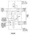
- FIG. 6 shows a representative word line fuse logic 62 or 64 and an associated spare word line fuse logic 72 or 74.
- Fuse 462 is intact if the depicted regular word line pair is to be used, and fuse 472 is intact if the depicted spare word line pair is not to be used. This enables the NOR gates in the depicted regular word line fuse logic and cuts off the associated N-channel transistors in the spare fuse logic.
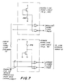
- FIG. 7 shows representative word line fuse logic 66 and associated spare word line fuse logic 76.
- Word line fuse logic 66 is similar to word line fuse logic 62 or 64 in FIG. 6. Fuse 466 is intact unless the associated regular word line pair is not to be used, and fuse 476 is intact unless the associated spare word line pair is to be used.
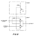
- FIG. 8 shows the combination of a simple fuse circuit 442 and a multiplexer circuit 444 which can be used wherever a multiplexer is required to implement either direct replacement (as in FIG. 1) or shifting replacement (as in FIG. 4). (Note that the direction of information flow in multiplexer 444 can be reversed so that the alternate and regular inputs become alternate and regular outputs, respectively, and so that the output becomes the input.)
- multiplexer 444 can be used for any of multiplexers 44 or 46 in FIG. 1a (with the control signal coming from one of fuse logics 32 rather than from fuse circuit 442) or any of multiplexers 44, 46, 234, 264, 334, 344, or 364 in FIG. 4 (with the control signal coming from the source indicated in that FIG.).
- Fuse logics such as 230, 232, 262, 330, and 362 can be similar to fuse logic 442.
- the control signal applied to multiplexer 444 is high (fuse 446 intact), the normal input signal is applied to the output and the alternate input signal is blocked.
- the control signal applied to multiplexer 444 is low (fuse 446 blown), the alternate input is applied to the output and the normal input signal is blocked.
Landscapes
- Physics & Mathematics (AREA)
- Mathematical Physics (AREA)
- Engineering & Computer Science (AREA)
- Computer Hardware Design (AREA)
- Computing Systems (AREA)
- General Engineering & Computer Science (AREA)
- Computer Networks & Wireless Communication (AREA)
- Logic Circuits (AREA)
- For Increasing The Reliability Of Semiconductor Memories (AREA)
- Design And Manufacture Of Integrated Circuits (AREA)
Claims (14)
- Programmierbare logische Schaltung (10), die eine Vielzahl von ersten Leitern und eine Vielzahl von zweiten Leitern besitzt, wobei jeder der zweiten Leiter programmierbar verbindbar ist zu jedem der ersten Leiter, um auf jedem der zweiten Leiter ein Signal zu erzeugen, welches eine logische Funktion der Signale des mit dem zweiten Leiter verbundenen ersten Leiters ist, und die programmierbare logische Schaltung (10) die Funktionselemente aufweist:
vorprogrammierbare Einrichtungen (262, 230, 232), die verbunden mit jedem Leiter aus mindestens einer der Vielzahlen der Leiter ein Hinweissignal erzeugen, ob oder ob nicht der verbundene Leiter zu benutzen ist, wobei die Vielzahl der mit den vorprogrammierbaren Einrichtungen (262, 230, 232) verbundenen Leiter einen Ersatzleiter für den Fall beinhaltet, daß einer der anderen Leiter auf derselben Vielzahl, welche im folgenden als reguläre Leiter bezeichnet werden, nicht zu benutzen ist, und eine Vorrichtung (264, 234, 36) zur Umlenkung des Signals, die reagiert auf ein Hinweissignal der vorprogrammierbaren Einrichtungen (262, 230, 232), daß ein bestimmter regulärer Leiter nicht zu benutzen ist,
dadurch gekennzeichnet, daß
die regulären Leiter sich in einer angeordneten Folge auf der programmierbaren logischen Schaltung (10) befinden und die Vorrichtung (264; 234) zur Umlenkung des Signals dazu dient, die an dem regulären Leiter und irgendwelchen regulären Leitern auf einer Seite des regulären Leiters in der angeordneten Folge anliegenden Signale hin zu dem entsprechenden in der Richtung des Schiebens nachfolgenden regulären Leiter zu verschieben, dabei ist das letzte verschobene Signal, das benutzt wird, von dem letzten der regulären Leiter hin zu dem Ersatzleiter umgelenkt. - Programmierbare logische Schaltung (10) nach Anspruch 1, dadurch gekennzeichnet, daß der Ersatzleiter sich in Richtung des Schiebens nach dem Ende der angeordneten Folge befindet.
- Programmierbare logische Schaltung (10) nach Anspruch 1 oder Anspruch 2, dadurch gekennzeichnet, daß die vorprogrammierbare Einrichtung (262) und die Vorrichtung (264) zur Umlenkung des Signals mit ersten Leitern verbunden sind und dabei die programmierbare logische Schaltung (10) ferner aufweist:
zweite vorprogrammierbare Einrichtungen (230, 232), die verbunden mit jedem der zweiten Leiter, ein Hinweissignal erzeugen, ob oder ob nicht der verbundene zweite Leiter zu benutzen ist, und eine zweite Vorrichtung (234, 36) zur Umlenkung des Signals, die reagiert auf ein Hinweissignal der zweiten vorprogrammierten Einrichtung, daß ein bestimmter zweiter Leiter nicht zu benutzen ist, wobei die zweite Vorrichtung (234, 36) zur Umlenkung des Signals dazu dient, die an dem zweiten Leiter anliegenden Signale zu einem anderen zweiten Leiter umzulenken. - Programmierbare logische Schaltung (10) nach einem der vorhergehenden Ansprüche dadurch gekennzeichnet, daß die zweiten Leiter zu einer Vielzahl von Gruppen zusammengefaßt sind, wobei die programmierbare logische Schaltung (10) logische Vorrichtungen (24, 26, 28) beinhaltet, die die Signale auf mindestens einigen der zweiten Leiter in jeder Gruppe logisch kombinieren, um ein weiteres Signal zu erzeugen, das eine logische Funktion der kombinierten Signale ist, daß die vorprogrammierbare Einrichtung (230, 232) verbunden ist mit den zweiten Leitern und ein Hinweissignal erzeugt, ob oder ob nicht irgendeiner der zweiten Leiter in jeder Gruppe und in der dieser Gruppe zugeordneten logischen Vorrichtung (24, 26, 28) zu benutzen ist, und daß die Vorrichtung (234, 36) zur Umlenkung des Signals mit den zweiten Leitern verbunden ist und auf das Hinweissignal der vorprogrammierbaren Einrichtung (230, 232), daß eine bestimmte Gruppe und die damit verbundene logische Vorrichtung (24, 26, 28) nicht zu benutzen sind, mit Umlenken der an allen zweiten Leitern in dieser Gruppe anliegenden Signale hin zu einer anderen Gruppe reagiert.
- Programmierbare logische Schaltung (10) nach Anspruch 4, dadurch gekennzeichnet, daß die Gruppen eine Ersatzgruppe beinhalten für den Fall, daß eine der anderen Gruppen, welche im folgenden als reguläre Gruppen bezeichnet werden, nicht zu benutzen ist, und daß die Vorrichtung (234, 36) zur Umlenkung des Signals reagiert auf das Hinweissignal von der vorprogrammierbaren Einrichtung (230, 232, 330), daß irgendeiner der zweiten Leiter in einer bestimmten regulären Gruppe und die mit dieser Gruppe verbundenen logischen Einheiten (24, 26) nicht zu benutzen sind, und daß die Vorrichtung (234, 36) zur Umlenkung des Signals dazu dient, die an jedem der zweiten Leiter in dieser regulären Gruppe anliegenden Signale hin zu der Ersatzgruppe umzulenken.
- Programmierbare logische Schaltung (10) nach Anspruch 4 oder Anspruch 5, dadurch gekennzeichnet, daß die Vorrichtung zur Umlenkung des Signals dazu dient, die an allen zweiten Leitern in der regulären Gruppe und irgendwelchen regulären Gruppen auf einer Seite der regulären Gruppe in der angeordneten Folge anliegenden Signale hin zu der in der Richtung des Schiebens nachfolgenden regulären Gruppe zu verschieben, dabei werden die Signale der letzten verschobenen regulären Gruppe hin zu der Ersatzgruppe umgelenkt.
- Programmierbare logische Schaltung (10) nach Anspruch 5 oder Anspruch 6, dadurch gekennzeichnet, daß die Ersatzgruppe sich in Richtung des Schiebens nach dem Ende der angeordneten Folge befindet.
- Programmierbare logische Schaltung (10) nach einem der vorangehenden Ansprüche, dadurch gekennzeichnet, daß die vorprogrammierbare Einrichtung (262, 230, 232) eine Schaltung beinhaltet, die aus EPROM, EEPROM, Sicherung und Gegensicherung besteht.
- Programmierbare logische Schaltung (10) nach einem der vorangehenden Ansprüche, dadurch gekennzeichnet, daß die vorprogrammierbare Einrichtung (262, 230, 232) eine optothermisch veränderbare Vorrichtung beinhaltet.
- Programmierbare logische Schaltung (10) nach einem der vorangehenden Ansprüche, dadurch gekennzeichnet, daß diese Schaltung einen Programmodus aufweist, in dem ausgewählte Verbindungen zwischen den ersten und den zweiten Leitern durch Anlegen von Auswahlsignalen an die zu verbindenden ersten und zweiten Leiter hergestellt werden, und einen normalen Arbeitsmodus aufweist, in dem Eingangssignale an den ersten Leiter angelegt Ausgangssignale auf dem zweiten Leiter erzeugen, und daß die Vorrichtung (264, 234, 36) zur Umlenkung des Signals sowohl die Auswahlsignale als auch die an dem Leiter anliegenden Eingangssignale zu einem anderen Leiter in derselben Vielzahl umlenkt.
- Programmierbare logische Schaltung nach einem der vorangehenden Ansprüche, dadurch gekennzeichnet, daß die Schaltung zusätzlich eine Vielzahl von ersten Signalleitern und eine Vielzahl von zweiten Signalleitern aufweist, wobei jeder der zweiten Signalleiter programmierbar verbindbar ist zu irgendeinem ersten Signalleiter, daß eine weitere vorprogrammierbare Einrichtung (362; 330) in mindestens einer der Vielzahlen von Leitern verbunden ist mit jedem Leiter, um ein Ausgangssignal zu erzeugen, ob oder ob nicht der verbundene Leiter zu benutzen ist, weiterhin daß eine Vorrichtung (364; 334) zur Umlenkung des Signals reagiert auf ein Hinweissignal der weiteren vorprogrammierbaren Einrichtung, daß ein bestimmter Leiter nicht zum Umlenken der zu dem Leiter gehörenden Signale zu einem anderen Leiter in der Vielzahl zu benutzen ist, und daß die programmierbare logische Schaltung eine Vorrichtung (270, 60) aufweist, um wahlweise ein Signal von mindestens einigen der zweiten Leiter an einen entsprechenden ersten Leiter anzulegen.
- Verfahren zur Betreibung einer programmierbaren logischen Schaltung (10) bestehend aus einer Vielzahl von ersten Leitern und einer Vielzahl von zweiten Leitern, wobei jeder der zweiten Leiter programmierbar verbindbar ist zu jedem der ersten Leiter, um auf jedem der zweiten Leiter ein Signal zu erzeugen, welches eine logische Funktion der Signale des mit dem zweiten Leiter verbundenen ersten Leiters ist, und jede der Vielzahlen von Leitern einen Ersatzleiter beinhaltet für den Fall, daß einer der anderen Leiter in derselben Vielzahl, welche im folgenden als reguläre Leiter bezeichnet werden, nicht zu benutzen ist, dies Verfahren beinhaltet den Schritt: Bestimmen, ob irgendeiner der regulären Leiter in mindestens einer der Vielzahlen von Leitern nicht zu benutzen ist, und ist dadurch gekennzeichnet, daß die regulären Leiter sich in einer angeordneten Folge auf der programmierbaren logischen Schaltung (10) befinden, und daß das Verfahren ferner die Schritte zur Änderung der Schaltung, falls ein bestimmter regulärer Leiter nicht zu benutzen ist, was im vorhergehenden Schritt bestimmt wurde, beinhaltet, so daß die an diesem Leiter und jedem regulären Leiter auf einer Seite des regulären Leiters in der angeordneten Folge anliegenden Signale hin zu dem entsprechenden in der Richtung des Schiebens nachfolgenden Leiter verschoben werden, dabei werden die letzten verschobenen Signale von dem letzten regulären Leiters zu dem Ersatzleiter hin umgelenkt.
- Verfahren nach Anspruch 12, gekennzeichnet durch den Schritt wahlweise Programmsignale an den ersten und den zweiten Leiter der modifizierten Schaltung anzulegen, um die ersten und zweiten Leiter wahlweise zu verbinden und dabei die Schaltung zu programmieren, und alle an dem Leiter anliegenden Programmsignale automatisch zu dem anderen Leiter in derselben Vielzahl umzulenken.
- Verfahren nach Anspruch 13, gekennzeichnet durch den Schritt wahlweise Eingangssignaldaten an den ersten Leiter der programmierten modifizierten Schaltung anzulegen, um Ausgangssignaldaten auf dem zweiten Leitern zu erzeugen, und an dem Leiter anliegende Datensignale automatisch zu einem anderen Leiter in derselben Vielzahl umzulenken.
Applications Claiming Priority (2)
| Application Number | Priority Date | Filing Date | Title |
|---|---|---|---|
| US07/222,832 US4899067A (en) | 1988-07-22 | 1988-07-22 | Programmable logic devices with spare circuits for use in replacing defective circuits |
| US222832 | 1988-07-22 |
Publications (3)
| Publication Number | Publication Date |
|---|---|
| EP0351983A2 EP0351983A2 (de) | 1990-01-24 |
| EP0351983A3 EP0351983A3 (de) | 1991-05-15 |
| EP0351983B1 true EP0351983B1 (de) | 1996-11-13 |
Family
ID=22833888
Family Applications (1)
| Application Number | Title | Priority Date | Filing Date |
|---|---|---|---|
| EP89306839A Expired - Lifetime EP0351983B1 (de) | 1988-07-22 | 1989-07-06 | Geräte mit programmierbarer Logik mit Ersatzschaltungen zum Ersetzen defekter Schaltungen |
Country Status (4)
| Country | Link |
|---|---|
| US (1) | US4899067A (de) |
| EP (1) | EP0351983B1 (de) |
| JP (1) | JPH0273721A (de) |
| DE (1) | DE68927450D1 (de) |
Families Citing this family (149)
| Publication number | Priority date | Publication date | Assignee | Title |
|---|---|---|---|---|
| US5367208A (en) | 1986-09-19 | 1994-11-22 | Actel Corporation | Reconfigurable programmable interconnect architecture |
| US5140193A (en) * | 1990-03-27 | 1992-08-18 | Xilinx, Inc. | Programmable connector for programmable logic device |
| JPH04144000A (ja) * | 1990-10-03 | 1992-05-18 | Mitsubishi Electric Corp | 半導体記憶装置 |
| US5087839A (en) * | 1990-10-05 | 1992-02-11 | Unisys Corporation | Method of providing flexibility and alterability in VLSI gate array chips |
| US5384499A (en) * | 1991-04-25 | 1995-01-24 | Altera Corporation | High-density erasable programmable logic device architecture using multiplexer interconnections |
| US5241224A (en) * | 1991-04-25 | 1993-08-31 | Altera Corporation | High-density erasable programmable logic device architecture using multiplexer interconnections |
| US5268598A (en) * | 1991-04-25 | 1993-12-07 | Altera Corporation | High-density erasable programmable logic device architecture using multiplexer interconnections |
| US5260610A (en) * | 1991-09-03 | 1993-11-09 | Altera Corporation | Programmable logic element interconnections for programmable logic array integrated circuits |
| US6759870B2 (en) | 1991-09-03 | 2004-07-06 | Altera Corporation | Programmable logic array integrated circuits |
| JP2909328B2 (ja) * | 1992-11-02 | 1999-06-23 | 株式会社東芝 | フィールドプログラマブルゲートアレイ |
| US5434514A (en) * | 1992-11-19 | 1995-07-18 | Altera Corporation | Programmable logic devices with spare circuits for replacement of defects |
| US5498975A (en) * | 1992-11-19 | 1996-03-12 | Altera Corporation | Implementation of redundancy on a programmable logic device |
| US5483178A (en) * | 1993-03-29 | 1996-01-09 | Altera Corporation | Programmable logic device with logic block outputs coupled to adjacent logic block output multiplexers |
| US5539331A (en) * | 1993-05-10 | 1996-07-23 | Kabushiki Kaisha Toshiba | Field programmable gate array having transmission gates and semiconductor integrated circuit for programming connection of wires |
| US5486775A (en) * | 1993-11-22 | 1996-01-23 | Altera Corporation | Multiplexer structures for use in making controllable interconnections in integrated circuits. |
| US5369314A (en) * | 1994-02-22 | 1994-11-29 | Altera Corporation | Programmable logic device with redundant circuitry |
| US6294928B1 (en) | 1996-04-05 | 2001-09-25 | Altera Corporation | Programmable logic device with highly routable interconnect |
| US6181162B1 (en) | 1994-04-10 | 2001-01-30 | Altera Corporation | Programmable logic device with highly routable interconnect |
| USRE38651E1 (en) * | 1994-05-18 | 2004-11-09 | Altera Corporation | Variable depth and width memory device |
| US5689195A (en) * | 1995-05-17 | 1997-11-18 | Altera Corporation | Programmable logic array integrated circuit devices |
| IT1274925B (it) * | 1994-09-21 | 1997-07-29 | Texas Instruments Italia Spa | Architettura di memoria per dischi a stato solido |
| US5815726A (en) * | 1994-11-04 | 1998-09-29 | Altera Corporation | Coarse-grained look-up table architecture |
| US5525917A (en) * | 1994-12-16 | 1996-06-11 | Altera Corporation | Sense amplifier with feedback and stabilization |
| US5850365A (en) * | 1994-12-16 | 1998-12-15 | Altera Corporation | Sense amplifier with individually optimized high and low power modes |
| US5537057A (en) * | 1995-02-14 | 1996-07-16 | Altera Corporation | Programmable logic array device with grouped logic regions and three types of conductors |
| GB2300946B (en) * | 1995-05-17 | 1999-10-20 | Altera Corp | Tri-statable input/output circuitry for programmable logic |
| US5614840A (en) * | 1995-05-17 | 1997-03-25 | Altera Corporation | Programmable logic array integrated circuits with segmented, selectively connectable, long interconnection conductors |
| US5909126A (en) | 1995-05-17 | 1999-06-01 | Altera Corporation | Programmable logic array integrated circuit devices with interleaved logic array blocks |
| US5541530A (en) * | 1995-05-17 | 1996-07-30 | Altera Corporation | Programmable logic array integrated circuits with blocks of logic regions grouped into super-blocks |
| US5900743A (en) * | 1995-05-17 | 1999-05-04 | Altera Corporation | Programmable logic array devices with interconnect lines of various lengths |
| US5543730A (en) * | 1995-05-17 | 1996-08-06 | Altera Corporation | Techniques for programming programmable logic array devices |
| US5592106A (en) * | 1995-05-17 | 1997-01-07 | Altera Corporation | Programmable logic array integrated circuits with interconnection conductors of overlapping extent |
| US5543732A (en) * | 1995-05-17 | 1996-08-06 | Altera Corporation | Programmable logic array devices with interconnect lines of various lengths |
| US5963049A (en) | 1995-05-17 | 1999-10-05 | Altera Corporation | Programmable logic array integrated circuit architectures |
| US5659717A (en) * | 1995-07-31 | 1997-08-19 | Altera Corporation | Methods for partitioning circuits in order to allocate elements among multiple circuit groups |
| US5581501A (en) * | 1995-08-17 | 1996-12-03 | Altera Corporation | Nonvolatile SRAM cells and cell arrays |
| US5565793A (en) * | 1995-08-22 | 1996-10-15 | Altera Corporation | Programmable logic array integrated circuit devices with regions of enhanced interconnectivity |
| US5764080A (en) * | 1995-08-24 | 1998-06-09 | Altera Corporation | Input/output interface circuitry for programmable logic array integrated circuit devices |
| US5631576A (en) * | 1995-09-01 | 1997-05-20 | Altera Corporation | Programmable logic array integrated circuit devices with flexible carry chains |
| US5821773A (en) * | 1995-09-06 | 1998-10-13 | Altera Corporation | Look-up table based logic element with complete permutability of the inputs to the secondary signals |
| US5729495A (en) * | 1995-09-29 | 1998-03-17 | Altera Corporation | Dynamic nonvolatile memory cell |
| US5744991A (en) * | 1995-10-16 | 1998-04-28 | Altera Corporation | System for distributing clocks using a delay lock loop in a programmable logic circuit |
| US5970255A (en) | 1995-10-16 | 1999-10-19 | Altera Corporation | System for coupling programmable logic device to external circuitry which selects a logic standard and uses buffers to modify output and input signals accordingly |
| US5670895A (en) * | 1995-10-19 | 1997-09-23 | Altera Corporation | Routing connections for programmable logic array integrated circuits |
| US5592102A (en) * | 1995-10-19 | 1997-01-07 | Altera Corporation | Means and apparatus to minimize the effects of silicon processing defects in programmable logic devices |
| US5793246A (en) | 1995-11-08 | 1998-08-11 | Altera Corporation | High voltage pump scheme incorporating an overlapping clock |
| US5672985A (en) * | 1995-12-18 | 1997-09-30 | Altera Corporation | Programmable logic array integrated circuits with carry and/or cascade rings |
| US5767734A (en) * | 1995-12-21 | 1998-06-16 | Altera Corporation | High-voltage pump with initiation scheme |
| US5894228A (en) * | 1996-01-10 | 1999-04-13 | Altera Corporation | Tristate structures for programmable logic devices |
| US6882177B1 (en) | 1996-01-10 | 2005-04-19 | Altera Corporation | Tristate structures for programmable logic devices |
| US5691653A (en) * | 1996-01-16 | 1997-11-25 | Altera Corporation | Product term based programmable logic array devices with reduced control memory requirements |
| US5787009A (en) * | 1996-02-20 | 1998-07-28 | Altera Corporation | Methods for allocating circuit design portions among physical circuit portions |
| US5768372A (en) * | 1996-03-13 | 1998-06-16 | Altera Corporation | Method and apparatus for securing programming data of a programmable logic device |
| US6005806A (en) | 1996-03-14 | 1999-12-21 | Altera Corporation | Nonvolatile configuration cells and cell arrays |
| US5694058A (en) * | 1996-03-20 | 1997-12-02 | Altera Corporation | Programmable logic array integrated circuits with improved interconnection conductor utilization |
| US5835998A (en) * | 1996-04-04 | 1998-11-10 | Altera Corporation | Logic cell for programmable logic devices |
| US5872463A (en) * | 1996-04-04 | 1999-02-16 | Altera Corporation | Routing in programmable logic devices using shared distributed programmable logic connectors |
| US5869979A (en) * | 1996-04-05 | 1999-02-09 | Altera Corporation | Technique for preconditioning I/Os during reconfiguration |
| US6034540A (en) | 1997-04-08 | 2000-03-07 | Altera Corporation | Programmable logic integrated circuit architecture incorporating a lonely register |
| US6107822A (en) | 1996-04-09 | 2000-08-22 | Altera Corporation | Logic element for a programmable logic integrated circuit |
| US5986465A (en) * | 1996-04-09 | 1999-11-16 | Altera Corporation | Programmable logic integrated circuit architecture incorporating a global shareable expander |
| US5939790A (en) * | 1996-04-09 | 1999-08-17 | Altera Corporation | Integrated circuit pad structures |
| US5949710A (en) | 1996-04-10 | 1999-09-07 | Altera Corporation | Programmable interconnect junction |
| US5998295A (en) * | 1996-04-10 | 1999-12-07 | Altera Corporation | Method of forming a rough region on a substrate |
| US5977791A (en) | 1996-04-15 | 1999-11-02 | Altera Corporation | Embedded memory block with FIFO mode for programmable logic device |
| US6147511A (en) | 1996-05-28 | 2000-11-14 | Altera Corporation | Overvoltage-tolerant interface for integrated circuits |
| US6025737A (en) * | 1996-11-27 | 2000-02-15 | Altera Corporation | Circuitry for a low internal voltage integrated circuit |
| US6384630B2 (en) | 1996-06-05 | 2002-05-07 | Altera Corporation | Techniques for programming programmable logic array devices |
| US5715197A (en) | 1996-07-29 | 1998-02-03 | Xilinx, Inc. | Multiport RAM with programmable data port configuration |
| US5959891A (en) | 1996-08-16 | 1999-09-28 | Altera Corporation | Evaluation of memory cell characteristics |
| US5771264A (en) * | 1996-08-29 | 1998-06-23 | Altera Corporation | Digital delay lock loop for clock signal frequency multiplication |
| US6236597B1 (en) | 1996-09-16 | 2001-05-22 | Altera Corporation | Nonvolatile memory cell with multiple gate oxide thicknesses |
| US6018476A (en) * | 1996-09-16 | 2000-01-25 | Altera Corporation | Nonvolatile configuration cells and cell arrays |
| US5880597A (en) * | 1996-09-18 | 1999-03-09 | Altera Corporation | Interleaved interconnect for programmable logic array devices |
| US5844854A (en) * | 1996-09-18 | 1998-12-01 | Altera Corporation | Programmable logic device with two dimensional memory addressing |
| US5914904A (en) * | 1996-10-01 | 1999-06-22 | Altera Corporation | Compact electrically erasable memory cells and arrays |
| US5977793A (en) * | 1996-10-10 | 1999-11-02 | Altera Corporation | Programmable logic device with hierarchical interconnection resources |
| US5999016A (en) * | 1996-10-10 | 1999-12-07 | Altera Corporation | Architectures for programmable logic devices |
| US6300794B1 (en) | 1996-10-10 | 2001-10-09 | Altera Corporation | Programmable logic device with hierarchical interconnection resources |
| US5942914A (en) * | 1996-10-25 | 1999-08-24 | Altera Corporation | PLD with split multiplexed inputs from global conductors |
| US6034536A (en) * | 1997-02-05 | 2000-03-07 | Altera Corporation | Redundancy circuitry for logic circuits |
| US6091258A (en) * | 1997-02-05 | 2000-07-18 | Altera Corporation | Redundancy circuitry for logic circuits |
| GB2321989B (en) * | 1997-02-05 | 2000-10-18 | Altera Corp | Redundancy circuitry for logic circuits |
| US7148722B1 (en) | 1997-02-20 | 2006-12-12 | Altera Corporation | PCI-compatible programmable logic devices |
| US5999015A (en) * | 1997-02-20 | 1999-12-07 | Altera Corporation | Logic region resources for programmable logic devices |
| US5982195A (en) * | 1997-02-20 | 1999-11-09 | Altera Corporation | Programmable logic device architectures |
| US6127844A (en) | 1997-02-20 | 2000-10-03 | Altera Corporation | PCI-compatible programmable logic devices |
| US6184710B1 (en) | 1997-03-20 | 2001-02-06 | Altera Corporation | Programmable logic array devices with enhanced interconnectivity between adjacent logic regions |
| DE69802927T2 (de) * | 1997-05-23 | 2002-08-08 | Altera Corp. ( A Delaware Corporation), San Jose | Redundanzschaltung für programmierbare logikanordnung mit verschachtelten eingangsschaltkreisen |
| US6239612B1 (en) | 1997-08-20 | 2001-05-29 | Altera Corporation | Programmable I/O cells with multiple drivers |
| US6130555A (en) * | 1997-10-13 | 2000-10-10 | Altera Corporation | Driver circuitry for programmable logic devices |
| US6052327A (en) * | 1997-10-14 | 2000-04-18 | Altera Corporation | Dual-port programmable logic device variable depth and width memory array |
| US6107825A (en) * | 1997-10-16 | 2000-08-22 | Altera Corporation | Input/output circuitry for programmable logic devices |
| US6288970B1 (en) | 1997-10-16 | 2001-09-11 | Altera Corporation | Programmable logic device memory array circuit having combinable single-port memory arrays |
| US6084427A (en) * | 1998-05-19 | 2000-07-04 | Altera Corporation | Programmable logic devices with enhanced multiplexing capabilities |
| US6191998B1 (en) | 1997-10-16 | 2001-02-20 | Altera Corporation | Programmable logic device memory array circuit having combinable single-port memory arrays |
| US6107824A (en) * | 1997-10-16 | 2000-08-22 | Altera Corporation | Circuitry and methods for internal interconnection of programmable logic devices |
| US6121790A (en) | 1997-10-16 | 2000-09-19 | Altera Corporation | Programmable logic device with enhanced multiplexing capabilities in interconnect resources |
| US6255850B1 (en) | 1997-10-28 | 2001-07-03 | Altera Corporation | Integrated circuit with both clamp protection and high impedance protection from input overshoot |
| US6172520B1 (en) * | 1997-12-30 | 2001-01-09 | Xilinx, Inc. | FPGA system with user-programmable configuration ports and method for reconfiguring the FPGA |
| US6167558A (en) * | 1998-02-20 | 2000-12-26 | Xilinx, Inc. | Method for tolerating defective logic blocks in programmable logic devices |
| US6201404B1 (en) | 1998-07-14 | 2001-03-13 | Altera Corporation | Programmable logic device with redundant circuitry |
| US6184707B1 (en) | 1998-10-07 | 2001-02-06 | Altera Corporation | Look-up table based logic element with complete permutability of the inputs to the secondary signals |
| US6507216B1 (en) | 1998-11-18 | 2003-01-14 | Altera Corporation | Efficient arrangement of interconnection resources on programmable logic devices |
| US6215326B1 (en) | 1998-11-18 | 2001-04-10 | Altera Corporation | Programmable logic device architecture with super-regions having logic regions and a memory region |
| US6407576B1 (en) | 1999-03-04 | 2002-06-18 | Altera Corporation | Interconnection and input/output resources for programmable logic integrated circuit devices |
| US6255845B1 (en) * | 1999-11-16 | 2001-07-03 | Advanced Micro Devices, Inc. | Efficient use of spare gates for post-silicon debug and enhancements |
| US6600337B2 (en) | 2000-04-26 | 2003-07-29 | Altera Corporation | Line segmentation in programmable logic devices having redundancy circuitry |
| US7484081B1 (en) | 2000-10-10 | 2009-01-27 | Altera Corporation | Method and apparatus for protecting designs in SRAM-based programmable logic devices |
| US7127697B1 (en) | 2001-08-07 | 2006-10-24 | Xilinx, Inc. | Methods of utilizing programmable logic devices having localized defects in application-specific products |
| US6664808B2 (en) * | 2001-08-07 | 2003-12-16 | Xilinx, Inc. | Method of using partially defective programmable logic devices |
| US6965249B2 (en) * | 2001-10-15 | 2005-11-15 | Altera Corporation | Programmable logic device with redundant circuitry |
| US7047465B1 (en) | 2002-02-28 | 2006-05-16 | Xilinx, Inc. | Methods for using defective programmable logic devices by customizing designs based on recorded defects |
| US7143295B1 (en) | 2002-07-18 | 2006-11-28 | Xilinx, Inc. | Methods and circuits for dedicating a programmable logic device for use with specific designs |
| US7111213B1 (en) | 2002-12-10 | 2006-09-19 | Altera Corporation | Failure isolation and repair techniques for integrated circuits |
| US7111110B1 (en) | 2002-12-10 | 2006-09-19 | Altera Corporation | Versatile RAM for programmable logic device |
| US7062685B1 (en) | 2002-12-11 | 2006-06-13 | Altera Corporation | Techniques for providing early failure warning of a programmable circuit |
| US7024327B1 (en) | 2002-12-18 | 2006-04-04 | Altera Corporation | Techniques for automatically generating tests for programmable circuits |
| US7058534B1 (en) | 2003-03-19 | 2006-06-06 | Altera Corporation | Method and apparatus for application specific test of PLDs |
| US7215140B1 (en) | 2003-05-30 | 2007-05-08 | Altera Corporation | Programmable logic device having regions of non-repairable circuitry within an array of repairable circuitry and associated configuration hardware and method |
| US7216277B1 (en) | 2003-11-18 | 2007-05-08 | Xilinx, Inc. | Self-repairing redundancy for memory blocks in programmable logic devices |
| US7180324B2 (en) | 2004-05-28 | 2007-02-20 | Altera Corporation | Redundancy structures and methods in a programmable logic device |
| US8612772B1 (en) | 2004-09-10 | 2013-12-17 | Altera Corporation | Security core using soft key |
| US8566616B1 (en) | 2004-09-10 | 2013-10-22 | Altera Corporation | Method and apparatus for protecting designs in SRAM-based programmable logic devices and the like |
| US7412635B1 (en) | 2004-10-01 | 2008-08-12 | Xilinx, Inc. | Utilizing multiple bitstreams to avoid localized defects in partially defective programmable integrated circuits |
| US7284229B1 (en) | 2004-10-01 | 2007-10-16 | Xilinx, Inc. | Multiple bitstreams enabling the use of partially defective programmable integrated circuits while avoiding localized defects therein |
| US7251804B1 (en) | 2004-10-01 | 2007-07-31 | Xilinx, Inc. | Structures and methods of overcoming localized defects in programmable integrated circuits by routing during the programming thereof |
| US7424655B1 (en) | 2004-10-01 | 2008-09-09 | Xilinx, Inc. | Utilizing multiple test bitstreams to avoid localized defects in partially defective programmable integrated circuits |
| JP2006134997A (ja) * | 2004-11-04 | 2006-05-25 | Fujitsu Ltd | プログラム可能論理デバイス |
| US7277346B1 (en) | 2004-12-14 | 2007-10-02 | Altera Corporation | Method and system for hard failure repairs in the field |
| US7265573B1 (en) | 2004-12-18 | 2007-09-04 | Altera Corporation | Methods and structures for protecting programming data for a programmable logic device |
| US7394708B1 (en) | 2005-03-18 | 2008-07-01 | Xilinx, Inc. | Adjustable global tap voltage to improve memory cell yield |
| EP1995663A1 (de) * | 2007-05-22 | 2008-11-26 | Panasonic Corporation | System und Verfahren zur lokalen Erzeugung von Programmdaten in einer programmierbaren Vorrichtung |
| US7810059B1 (en) | 2007-10-11 | 2010-10-05 | Xilinx, Inc. | Methods of enabling the validation of an integrated circuit adapted to receive one of a plurality of configuration bitstreams |
| US7853916B1 (en) | 2007-10-11 | 2010-12-14 | Xilinx, Inc. | Methods of using one of a plurality of configuration bitstreams for an integrated circuit |
| US7619438B1 (en) | 2007-10-11 | 2009-11-17 | Xilinx, Inc. | Methods of enabling the use of a defective programmable device |
| US7902855B1 (en) * | 2010-03-03 | 2011-03-08 | Altera Corporation | Repairable IO in an integrated circuit |
| US8461863B2 (en) | 2011-04-29 | 2013-06-11 | Altera Corporation | Method and apparatus for securing a programmable device using a kill switch |
| US8627105B2 (en) | 2011-04-29 | 2014-01-07 | Altera Corporation | Method and apparatus for securing programming data of a programmable device |
| US8736299B1 (en) | 2011-04-29 | 2014-05-27 | Altera Corporation | Setting security features of programmable logic devices |
| US8719957B2 (en) | 2011-04-29 | 2014-05-06 | Altera Corporation | Systems and methods for detecting and mitigating programmable logic device tampering |
| US8539420B2 (en) * | 2011-07-05 | 2013-09-17 | Xilinx, Inc. | Method and apparatus for self-annealing multi-die interconnect redundancy control |
| US9236864B1 (en) | 2012-01-17 | 2016-01-12 | Altera Corporation | Stacked integrated circuit with redundancy in die-to-die interconnects |
| US9026873B2 (en) | 2013-07-23 | 2015-05-05 | Altera Coporation | Method and apparatus for securing configuration scan chains of a programmable device |
| US9692422B2 (en) | 2014-03-17 | 2017-06-27 | Nec Corporation | Programmable logic integrated circuit |
| US10044355B2 (en) | 2015-05-28 | 2018-08-07 | Nec Corporation | Reconfigurable circuit with crossbar switches including non-volatile resistive switches |
| US10740435B2 (en) | 2015-05-29 | 2020-08-11 | Nec Corporation | Programmable logic integrated circuit, design support system, and configuration method |
| JP6485225B2 (ja) * | 2015-05-29 | 2019-03-20 | 日本電気株式会社 | プログラマブル論理集積回路 |
| CN112510054B (zh) | 2019-09-16 | 2024-07-05 | 联华电子股份有限公司 | 影像传感器及其制造方法 |
Family Cites Families (13)
| Publication number | Priority date | Publication date | Assignee | Title |
|---|---|---|---|---|
| US3566153A (en) * | 1969-04-30 | 1971-02-23 | Texas Instruments Inc | Programmable sequential logic |
| US4124899A (en) * | 1977-05-23 | 1978-11-07 | Monolithic Memories, Inc. | Programmable array logic circuit |
| DE3036869C2 (de) * | 1979-10-01 | 1985-09-05 | Hitachi, Ltd., Tokio/Tokyo | Integrierte Halbleiterschaltung und Schaltkreisaktivierverfahren |
| DE3015992A1 (de) * | 1980-04-25 | 1981-11-05 | Ibm Deutschland Gmbh, 7000 Stuttgart | Programmierbare logische anordnung |
| JPS6093700A (ja) * | 1983-10-26 | 1985-05-25 | Hitachi Ltd | ライン切換回路およびそれを用いた半導体記憶装置 |
| US4551814A (en) * | 1983-12-12 | 1985-11-05 | Aerojet-General Corporation | Functionally redundant logic network architectures |
| US4713792A (en) * | 1985-06-06 | 1987-12-15 | Altera Corporation | Programmable macrocell using eprom or eeprom transistors for architecture control in programmable logic circuits |
| US4617479B1 (en) * | 1984-05-03 | 1993-09-21 | Altera Semiconductor Corp. | Programmable logic array device using eprom technology |
| US4609986A (en) * | 1984-06-14 | 1986-09-02 | Altera Corporation | Programmable logic array device using EPROM technology |
| US4677318A (en) * | 1985-04-12 | 1987-06-30 | Altera Corporation | Programmable logic storage element for programmable logic devices |
| US4703206A (en) * | 1985-11-19 | 1987-10-27 | Signetics Corporation | Field-programmable logic device with programmable foldback to control number of logic levels |
| US4700187A (en) * | 1985-12-02 | 1987-10-13 | Concurrent Logic, Inc. | Programmable, asynchronous logic cell and array |
| JPS632351A (ja) * | 1986-06-20 | 1988-01-07 | Sharp Corp | 半導体装置 |
-
1988
- 1988-07-22 US US07/222,832 patent/US4899067A/en not_active Expired - Lifetime
-
1989
- 1989-07-06 EP EP89306839A patent/EP0351983B1/de not_active Expired - Lifetime
- 1989-07-06 DE DE68927450T patent/DE68927450D1/de not_active Expired - Lifetime
- 1989-07-20 JP JP1186183A patent/JPH0273721A/ja active Pending
Also Published As
| Publication number | Publication date |
|---|---|
| EP0351983A3 (de) | 1991-05-15 |
| JPH0273721A (ja) | 1990-03-13 |
| EP0351983A2 (de) | 1990-01-24 |
| US4899067A (en) | 1990-02-06 |
| DE68927450D1 (de) | 1996-12-19 |
Similar Documents
| Publication | Publication Date | Title |
|---|---|---|
| EP0351983B1 (de) | Geräte mit programmierbarer Logik mit Ersatzschaltungen zum Ersetzen defekter Schaltungen | |
| US5600265A (en) | Programmable interconnect architecture | |
| US4910417A (en) | Universal logic module comprising multiplexers | |
| US4873459A (en) | Programmable interconnect architecture | |
| US5498975A (en) | Implementation of redundancy on a programmable logic device | |
| US6344755B1 (en) | Programmable logic device with redundant circuitry | |
| EP0034070B1 (de) | Fehler tolerierendes Speichersystem | |
| US5459342A (en) | Field programmable gate array with spare circuit block | |
| US5187393A (en) | Reconfigurable programmable interconnect architecture | |
| US5369314A (en) | Programmable logic device with redundant circuitry | |
| US4857774A (en) | Testing apparatus and diagnostic method for use with programmable interconnect architecture | |
| US5015885A (en) | Reconfigurable programmable interconnect architecture | |
| US5172014A (en) | Programmable interconnect architecture | |
| US5925920A (en) | Techniques and circuits for high yield improvements in programmable devices using redundant routing resources | |
| JPH05198683A (ja) | ラッチ支援ヒューズテスト回路及びラッチ支援ヒューズテスト方法 | |
| US6077211A (en) | Circuits and methods for selectively coupling redundant elements into an integrated circuit | |
| US4837765A (en) | Test control circuit for integrated circuit | |
| US7355910B2 (en) | Semiconductor memory device with shift redundancy circuits | |
| KR19980071793A (ko) | 전기적으로 프로그램 가능한 리던던시를 지닌 반도체 기억 장치 | |
| US20040105289A1 (en) | Method and apparatus for replacing defective rows in a semiconductor memory array | |
| US6621749B2 (en) | Integrated circuit memory devices providing per-bit redundancy and methods of operating same | |
| KR19990023677A (ko) | 용장 회로를 구비한 반도체 기억 장치 | |
| KR0172382B1 (ko) | 메모리셀 어레이 블럭의 재배치가 가능한 반도체 메모리 장치 | |
| JPH06176596A (ja) | 冗長メモリ・ブロックを備えた集積回路メモリ・ディバイス | |
| GB2321989A (en) | Redundancy circuitry for logic circuits |
Legal Events
| Date | Code | Title | Description |
|---|---|---|---|
| PUAI | Public reference made under article 153(3) epc to a published international application that has entered the european phase |
Free format text: ORIGINAL CODE: 0009012 |
|
| AK | Designated contracting states |
Kind code of ref document: A2 Designated state(s): DE FR GB IT NL |
|
| PUAL | Search report despatched |
Free format text: ORIGINAL CODE: 0009013 |
|
| AK | Designated contracting states |
Kind code of ref document: A3 Designated state(s): DE FR GB IT NL |
|
| 17P | Request for examination filed |
Effective date: 19911022 |
|
| RAP1 | Party data changed (applicant data changed or rights of an application transferred) |
Owner name: ALTERA CORPORATION |
|
| 17Q | First examination report despatched |
Effective date: 19940421 |
|
| GRAH | Despatch of communication of intention to grant a patent |
Free format text: ORIGINAL CODE: EPIDOS IGRA |
|
| GRAH | Despatch of communication of intention to grant a patent |
Free format text: ORIGINAL CODE: EPIDOS IGRA |
|
| GRAA | (expected) grant |
Free format text: ORIGINAL CODE: 0009210 |
|
| AK | Designated contracting states |
Kind code of ref document: B1 Designated state(s): DE FR GB IT NL |
|
| PG25 | Lapsed in a contracting state [announced via postgrant information from national office to epo] |
Ref country code: IT Free format text: LAPSE BECAUSE OF FAILURE TO SUBMIT A TRANSLATION OF THE DESCRIPTION OR TO PAY THE FEE WITHIN THE PRESCRIBED TIME-LIMIT;WARNING: LAPSES OF ITALIAN PATENTS WITH EFFECTIVE DATE BEFORE 2007 MAY HAVE OCCURRED AT ANY TIME BEFORE 2007. THE CORRECT EFFECTIVE DATE MAY BE DIFFERENT FROM THE ONE RECORDED. Effective date: 19961113 Ref country code: FR Effective date: 19961113 Ref country code: NL Free format text: LAPSE BECAUSE OF FAILURE TO SUBMIT A TRANSLATION OF THE DESCRIPTION OR TO PAY THE FEE WITHIN THE PRESCRIBED TIME-LIMIT Effective date: 19961113 |
|
| REF | Corresponds to: |
Ref document number: 68927450 Country of ref document: DE Date of ref document: 19961219 |
|
| PG25 | Lapsed in a contracting state [announced via postgrant information from national office to epo] |
Ref country code: DE Effective date: 19970214 |
|
| NLV1 | Nl: lapsed or annulled due to failure to fulfill the requirements of art. 29p and 29m of the patents act | ||
| EN | Fr: translation not filed | ||
| PLBE | No opposition filed within time limit |
Free format text: ORIGINAL CODE: 0009261 |
|
| STAA | Information on the status of an ep patent application or granted ep patent |
Free format text: STATUS: NO OPPOSITION FILED WITHIN TIME LIMIT |
|
| 26N | No opposition filed | ||
| REG | Reference to a national code |
Ref country code: GB Ref legal event code: 732E |
|
| REG | Reference to a national code |
Ref country code: GB Ref legal event code: IF02 |
|
| PGFP | Annual fee paid to national office [announced via postgrant information from national office to epo] |
Ref country code: GB Payment date: 20050614 Year of fee payment: 17 |
|
| PG25 | Lapsed in a contracting state [announced via postgrant information from national office to epo] |
Ref country code: GB Free format text: LAPSE BECAUSE OF NON-PAYMENT OF DUE FEES Effective date: 20060706 |
|
| GBPC | Gb: european patent ceased through non-payment of renewal fee |
Effective date: 20060706 |