EP0351955A2 - Mehrprozessoranordnungen mit kreuzweise abgefragten Schreib-in-Cachespeichern - Google Patents
Mehrprozessoranordnungen mit kreuzweise abgefragten Schreib-in-Cachespeichern Download PDFInfo
- Publication number
- EP0351955A2 EP0351955A2 EP89306227A EP89306227A EP0351955A2 EP 0351955 A2 EP0351955 A2 EP 0351955A2 EP 89306227 A EP89306227 A EP 89306227A EP 89306227 A EP89306227 A EP 89306227A EP 0351955 A2 EP0351955 A2 EP 0351955A2
- Authority
- EP
- European Patent Office
- Prior art keywords
- fetch
- cache
- memory
- buffer
- processors
- Prior art date
- Legal status (The legal status is an assumption and is not a legal conclusion. Google has not performed a legal analysis and makes no representation as to the accuracy of the status listed.)
- Granted
Links
Images


Classifications
-
- G—PHYSICS
- G06—COMPUTING; CALCULATING OR COUNTING
- G06F—ELECTRIC DIGITAL DATA PROCESSING
- G06F12/00—Accessing, addressing or allocating within memory systems or architectures
- G06F12/02—Addressing or allocation; Relocation
- G06F12/08—Addressing or allocation; Relocation in hierarchically structured memory systems, e.g. virtual memory systems
- G06F12/0802—Addressing of a memory level in which the access to the desired data or data block requires associative addressing means, e.g. caches
- G06F12/0806—Multiuser, multiprocessor or multiprocessing cache systems
- G06F12/0815—Cache consistency protocols
- G06F12/0817—Cache consistency protocols using directory methods
Definitions
- This invention relates to multiprocessor systems where each processor has a store-in cache and each processor can access the same main storage array via interconnection logic including system controller that while a line of data is being fetched it interrogates the other processor caches to insure that the requesting processor may indeed access this line and the system control element issues a release or cancel for each fetch and more particularly to a system where if the fetch array cycle completes before interrogation is complete a special buffering mechanism is invoked.
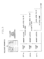
- Fig. 1 shows an organisation of a prior art multiprocessor system.
- the system has a multiple number of independent central processors (CP) 11a through 11n and a multiple number of independent memories, 13a through 13n.
- the memories shown in Fig. 1 are what make up what is referred to as the main storage array 13.
- the central processors (CPs) 11a through 11n and memories 13a through 13n are connected by interconnection logic 15.
- Each independent central processor (CP) in the system has a store-in cache.
- a store-in cache is described for example in U.S. Patent No. 4,136,386 of Annunziata et al. of International Business Machines Corporation, incorporated herein by reference. This is also described for example in Chiesa et al. U.S. Patent No.
- each processor contains its own buffer storage with directory and storage control and whenever such a processor fetches or stores data that is already resident in its own cache the access does not affect that which is in the distant control unit such as a system control unit or element (SCU or SCE) which normally contains a duplicate directory for each cache of the processor associated with it.
- SCU or SCE system control unit or element
- the address of the requested data will be compared against other cache directories that are resident in the system control element to see whether the requested data is resident in the cache of another processor. If the requested data is not resident in the cache of another processor the access request will be released. If the requested data is resident in the cache of another processor, a "cross-interrogate" hit signal will be used to prevent data from being read from the memories of the main storage array to the cache of the requesting processor and to signal the processor which has the data in its cache to cache out the data to the memory array.
- the access request to the main memory arrays will be placed on a first-in first-out queue form which will again be accessed at a later time.
- the system might use one or more system control elements each of which has two or more processors associated with the system.
- each system control element contains a copy of the directories of only its associated processors the address of the requested memory of the main memory array must be transmitted to each system control element for checking against all the directories to determine whether or not the requested data is already resident within the cache of a processor.
- Fig. 2 shows a system as described above where the interconnection logic includes multiple system control elements (SCE) and multiple memory controllers where a system control element and memory controller is coupled between multiple processors (CP) and a channel control element and a plurality of memories.
- This checking process is referred to as cross-interrogate (or XI). Since this cross-interrogate (XI) requires multiple cycles per request and can only service one request at a time, a cross-interrogate (XI) bottleneck will result during periods of high storage use.
- FIG. 3 is a timing chart where central processor 11a through 11n request data simultaneously from memories 13a through 13n of Fig. 1 respectively.
- the data transfer is impaired to central processor 11b and central processor 11c due to the cross-interrogate (XI) bottleneck.
- the symbol "X-check done” on the figure marks the point where cross-interrogate (XI) checking is complete.
- storage protect keys are provided in each system control element to enable each line access request to check a storage protect key (assigned to the page frame containing the requested line of data) to determine if access request file is a security requirement before the fetch access is allowed to be sent to the main storage.
- U.S. Patent No. 4,923,910 (Flusche et al.) incorporated herein by reference describes storage protect arrays provided in system control elements. Further the system control element also contains priority circuits that determine the priorities of the different type storage access request from the different processors so that access requests can be serially presented in the correct order to the main storage array.
- Each storage control element includes priority controls cross-interrogate and storage protect circuits, other processors storage controls, request control buses, and data buses between main storage and connected CPUs, I/O processors, and any remote circuit control elements. All the above can cause the delay.
- U.S. Patent No. 4,654,778 provides a means for reducing this access time to distant storage hierarchy while maintaining the essential functions of the storage access by providing a fast path (comprising a control and/or data bus) directly between a storage element being accessed and the requestor in parallel with the control and data busses normally provided between the requestor and the storage element in a hierarchy which may be remote from the requestor, for example main storage.
- the interconnection logic includes a second level cache with a second buffer storage directories and storage control which stores all of what is normally stored in the plurality of processors for quicker access between processors. While second level caches may aid somewhat in minimising and reducing the cross-interrogate bottlenecks, it adds another level of interrogation and is used both for fetch and to store data. This two level cache is always loaded and is not associated with a given memory. A second level cache or system as described in these patents also adds extra cost to the overall system.
- the present invention provides a multiprocessor system comprising main memory shared by a plurality of processors each having its own store-in cache and fetch logic operative in response to a fetch request by any processor that cannot be satisfied by its own cache to cross-interrogate the caches of the other processors and, in parallel, to instigate a fetch from main memory to the cache of the requesting processor which is not released until the cross-interrogation shows that main memory contains the most recent copy of the requested data, characterised in that a fetch buffer is provided between main memory and the processors and is logically connected to main memory, only when main memory has completed its fetch operation but no release has been generated, to receive the data from main memory, and to the requesting processor when release has been generated.
- One embodiment of the present invention disclosed hereinafter comprises a multiple number of independent memories in a main array and a multiple number of processors and an interconnection logic where each of the processors has a store-in cache where the most recent copy of the data does not always reside in the main storage array and that most recent copy of data can reside in the processor's cache and whenever a processor requests data logic checking must be done to determine where the latest copy of the data resides and when checking is done a release is sent. This checking is referred to as cross-interrogate.
- a fetch buffer for at least one memory of the array and located in the interconnection logic is selectively coupled between the memory and the processor to hold fetch data from memory when the memory is ready and cross-interrogation and other system checks are not complete and to unload the fetch buffer to the processor when the cross-interrogation and other checks are complete and the release is sent.
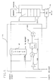
- FIG. 4 there is illustrated a multiprocessor system in accordance with a preferred embodiment of the present invention in which there is represented a plurality of central processors 21 through 24.
- Each of these processors includes its own private buffer storage and storage control and directory forming a store-in cache for that central processor.
- the system includes interconnection logic 20 and a plurality of memories 31 through 34 (main storage array)
- the interconnection logic 20 may include for example two system control elements (SCE) 41 and 43 and memory controllers (MC) 51 and 53.
- SCE system control elements
- MC memory controllers
- Each of the system control elements 41 and 43 include cross-interrogate circuits 41b, 43b and issuing/priority logic circuits 41a, 43a.
- the issuing/priority logic circuits 41a and 43a includes storage protection key circuits as well as priority control.
- fetch requests are produced out of the system control element from the logic circuits 41a and 43a to the memory control in the memory controllers 51 and 53 and to the cross interrogate logic circuits 41b and 43b to start cross-interrogation.
- SCE system control elements
- Data switches 41c and 43c control the data flow through the SCE.
- Main memories 31, 32, 33 and 34 for example may be addressed by any CP, such as CPs 21-24 via the data switches.
- the memory controller 51 provide local control for example for memories 31 and 32.
- the output from memory 31 is shown as being coupled to the processor 21 and the output from memory 32 is coupled to the processor 22, the output from memory 33 is coupled to processor 23 and the output from memory 34 is coupled to processor 24.
- these memories and processors are interconnected by address bus lines so any processor can be addressed to any memory and vice versa.
- memory 34 output can be passed to processor 21 via bus 110, data switch 43c, bus 60a, data switch 41c and bus 110. This can be via the fast path per U.S. Patent 4,654,778.
- the memory controller 51, 53 comprises a memory control circuit 51a, 53a which in response to the fetch request from the issuing/priority logic 41a or issuing/priority logic 43a provides a "memory ready" signal to corresponding buffer control 71, 72, 73 or 74.
- the memory control circuit counts the number of machine cycles known to access storage after fetch and provides the ready signal.
- the memory controller 51 includes fetch buffers 61, 63 and memory controller 53 includes a fetch buffers 65 and 67.
- Fetch buffers 61, 63, 65 and 67 are coupled to and buffer the output from memories 31, 32, 33 and 34 respectively.
- Cross-interrogate circuits 41b and 43b produce a release or cancel signal to buffer control circuits 71 through 74.
- a release signal is produced when the cross-interrogation verification that the main memory has the most current copy in the system and the requesting processor may indeed access the data as per the fetch request from the issuing priority logic.
- the buffer control logic in response to a "memory ready" signal from the memory control circuit loads the fetch buffer and after release signal will begin transferring data out of the buffer 61, 63, 65, and 67.
- a fetch request signal produces the memory ready signal to cause in the buffer control a counter to begin counting and loading data into the fetch buffer. For the example of a memory with a depth buffer of 1, a single cache line is loaded into the buffer 61.
- release signal is released before the memory ready the buffers 61, 63, 65 and 67 are bypassed via gates 91-94.
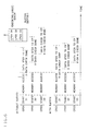
- FIG. 5 there is illustrated a diagram of a buffer control 71 which shows a double word counter 81.
- the output of the counter clocks the buffer sequentially to load the fetch buffer from the memory. This cancel is via a separate line from logics 41b or 43b. If the cross-interrogate issues a cancel, this cancel clears the double word counter and no output is provided from storage. If the output from the cross-interrogate circuit is a release signal from the SCE, this is used to shift data out of the fetch buffer. Also if there is a release following memory ready input signal this condition produces a select signal at the select gate 91 to output the data in the fetch buffer and apply the output from the fetch buffers to the central processors.
- This condition may be detected for example in the buffer control 71 by inverter 100, AND gate 101, one-shot latch 102 and AND gate 103. Only when a release occurs after a memory ready is AND gate 103 enabled to gate select gate 91 to the position to shift data out of the fetch buffer. This is the only condition in which gate 92 is in position so the output is coupled from the fetch buffer. Select gates 92 through 94 operate in the same manner. If the output from the cross-interrogate is a cancel, this clears the double word counter 81. When the double word counter is cleared, the contents of the buffer are unused and are overlayed during the next fetch request. Unless the "memory ready" signal is on to start the counter nothing is clocked into the buffer. If release signal occurs on or before the memory ready, the memory data bypasses the fetch buffer.
- the buffer is used on fetches (that is data coming out of the memory and going to a central processor (CP or channel CCE)).
- Each buffer has a defined depth.
- the fetch buffer holds only the portion of the cache line that can be transferred during cross-interrogation for example a cache line is 16 double words and a word is 72 bits long.
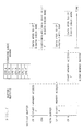
- Fig. 6 shows an example of a fetch buffer with a depth of one cache line and three central processors (CPs) fetching from different memories with and without the fetch buffers.
- the first processor CP21
- the fetch buffer CP22 and CP23 receives data sooner than without the buffer.
- the data is now being held in the interconnection logic instead of the memory cards of the main storage.
- the latency from the cross-interrogation (XI) due to data transfer is reduced.
- Another point which is not illustrated in the figures is that the memory will be available to handle another request sooner, since data was transferred out of the memory sooner.
- a fetch buffer shows timing improvement with a buffer depth of 2 and seven central processors (CPs) fetching.
- Central processors CP5 and CP6 are both fetching from a given memory.
- the cross-interrogation is backed up with respect to requests (see checking logic queue). Without the fetch buffer the central processor CP6 cannot start memory F until cross-interrogate checking is complete for central processor CP5's request. This leaves a large gap in time where the memory is sitting idle.
- CP6's request can be initiated as soon as CP5's request is done with the memory (but still waiting for cross-interrogate). Hence fully using the memory in a tightly coupled multiprocessor system.
- the present system speeds up the transfer of data to the requesting processor because the data is moved closer to the requestor and additional memory requests may be started sooner.
Landscapes
- Engineering & Computer Science (AREA)
- Theoretical Computer Science (AREA)
- Physics & Mathematics (AREA)
- General Engineering & Computer Science (AREA)
- General Physics & Mathematics (AREA)
- Memory System Of A Hierarchy Structure (AREA)
- Multi Processors (AREA)
Applications Claiming Priority (2)
| Application Number | Priority Date | Filing Date | Title |
|---|---|---|---|
| US07/222,678 US5032985A (en) | 1988-07-21 | 1988-07-21 | Multiprocessor system with memory fetch buffer invoked during cross-interrogation |
| US222678 | 1988-07-21 |
Publications (3)
| Publication Number | Publication Date |
|---|---|
| EP0351955A2 true EP0351955A2 (de) | 1990-01-24 |
| EP0351955A3 EP0351955A3 (de) | 1991-07-17 |
| EP0351955B1 EP0351955B1 (de) | 1995-09-20 |
Family
ID=22833233
Family Applications (1)
| Application Number | Title | Priority Date | Filing Date |
|---|---|---|---|
| EP89306227A Expired - Lifetime EP0351955B1 (de) | 1988-07-21 | 1989-06-20 | Mehrprozessoranordnungen mit kreuzweise abgefragten Schreib-in-Cachespeichern |
Country Status (4)
| Country | Link |
|---|---|
| US (1) | US5032985A (de) |
| EP (1) | EP0351955B1 (de) |
| JP (1) | JPH02255932A (de) |
| DE (1) | DE68924313T2 (de) |
Families Citing this family (28)
| Publication number | Priority date | Publication date | Assignee | Title |
|---|---|---|---|---|
| JPH0740247B2 (ja) * | 1989-06-20 | 1995-05-01 | 松下電器産業株式会社 | キャッシュメモリ装置 |
| DE68928980T2 (de) * | 1989-11-17 | 1999-08-19 | Texas Instruments Inc | Multiprozessor mit Koordinatenschalter zwischen Prozessoren und Speichern |
| US5197139A (en) * | 1990-04-05 | 1993-03-23 | International Business Machines Corporation | Cache management for multi-processor systems utilizing bulk cross-invalidate |
| US5493687A (en) | 1991-07-08 | 1996-02-20 | Seiko Epson Corporation | RISC microprocessor architecture implementing multiple typed register sets |
| US5539911A (en) | 1991-07-08 | 1996-07-23 | Seiko Epson Corporation | High-performance, superscalar-based computer system with out-of-order instruction execution |
| US5361368A (en) * | 1991-09-05 | 1994-11-01 | International Business Machines Corporation | Cross interrogate synchronization mechanism including logic means and delay register |
| DE69311330T2 (de) | 1992-03-31 | 1997-09-25 | Seiko Epson Corp | Befehlsablauffolgeplanung von einem risc-superskalarprozessor |
| EP0638183B1 (de) | 1992-05-01 | 1997-03-05 | Seiko Epson Corporation | Vorrichtung und verfahren zum befehlsabschluss in einem superskalaren prozessor. |
| US5426754A (en) * | 1992-05-26 | 1995-06-20 | International Business Machines Corporation | Cross-interrogate method and means for combined scaler and vector processing system |
| EP1107111A3 (de) | 1992-12-31 | 2002-02-06 | Seiko Epson Corporation | System und Verfahren zur Änderung der Namen von Registern |
| US5628021A (en) | 1992-12-31 | 1997-05-06 | Seiko Epson Corporation | System and method for assigning tags to control instruction processing in a superscalar processor |
| US5574868A (en) * | 1993-05-14 | 1996-11-12 | Intel Corporation | Bus grant prediction technique for a split transaction bus in a multiprocessor computer system |
| US5586297A (en) * | 1994-03-24 | 1996-12-17 | Hewlett-Packard Company | Partial cache line write transactions in a computing system with a write back cache |
| US5680338A (en) * | 1995-01-04 | 1997-10-21 | International Business Machines Corporation | Method and system for vector processing utilizing selected vector elements |
| US5890222A (en) * | 1995-01-04 | 1999-03-30 | International Business Machines Corporation | Method and system for addressing registers in a data processing unit in an indirect addressing mode |
| US5832533A (en) * | 1995-01-04 | 1998-11-03 | International Business Machines Corporation | Method and system for addressing registers in a data processing unit in an indexed addressing mode |
| US5887183A (en) * | 1995-01-04 | 1999-03-23 | International Business Machines Corporation | Method and system in a data processing system for loading and storing vectors in a plurality of modes |
| US6286076B1 (en) * | 1999-01-05 | 2001-09-04 | Sun Microsystems, Inc. | High speed memory-based buffer and system and method for use thereof |
| US6519649B1 (en) | 1999-11-09 | 2003-02-11 | International Business Machines Corporation | Multi-node data processing system and communication protocol having a partial combined response |
| US6671712B1 (en) | 1999-11-09 | 2003-12-30 | International Business Machines Corporation | Multi-node data processing system having a non-hierarchical interconnect architecture |
| US6591307B1 (en) | 1999-11-09 | 2003-07-08 | International Business Machines Corporation | Multi-node data processing system and method of queue management in which a queued operation is speculatively cancelled in response to a partial combined response |
| US6519665B1 (en) * | 1999-11-09 | 2003-02-11 | International Business Machines Corporation | Multi-node data processing system and communication protocol in which a stomp signal is propagated to cancel a prior request |
| US6848003B1 (en) | 1999-11-09 | 2005-01-25 | International Business Machines Corporation | Multi-node data processing system and communication protocol that route write data utilizing a destination ID obtained from a combined response |
| US6865695B2 (en) * | 2001-07-26 | 2005-03-08 | International Business Machines Corpoation | Robust system bus recovery |
| US7681105B1 (en) * | 2004-08-09 | 2010-03-16 | Bakbone Software, Inc. | Method for lock-free clustered erasure coding and recovery of data across a plurality of data stores in a network |
| US7681104B1 (en) * | 2004-08-09 | 2010-03-16 | Bakbone Software, Inc. | Method for erasure coding data across a plurality of data stores in a network |
| JP2011028343A (ja) * | 2009-07-22 | 2011-02-10 | Fujitsu Ltd | 演算処理装置、およびデータ転送方法 |
| KR101202691B1 (ko) * | 2010-07-08 | 2012-11-19 | 에스케이하이닉스 주식회사 | 데이터의 처리 장치 및 방법 |
Citations (2)
| Publication number | Priority date | Publication date | Assignee | Title |
|---|---|---|---|---|
| US4503497A (en) * | 1982-05-27 | 1985-03-05 | International Business Machines Corporation | System for independent cache-to-cache transfer |
| US4654778A (en) * | 1984-06-27 | 1987-03-31 | International Business Machines Corporation | Direct parallel path for storage accesses unloading common system path |
Family Cites Families (17)
| Publication number | Priority date | Publication date | Assignee | Title |
|---|---|---|---|---|
| JPS5226481B2 (de) * | 1973-08-15 | 1977-07-14 | ||
| US3866183A (en) * | 1973-08-31 | 1975-02-11 | Honeywell Inf Systems | Communications control apparatus for the use with a cache store |
| US3896419A (en) * | 1974-01-17 | 1975-07-22 | Honeywell Inf Systems | Cache memory store in a processor of a data processing system |
| US4136386A (en) * | 1977-10-06 | 1979-01-23 | International Business Machines Corporation | Backing store access coordination in a multi-processor system |
| JPS5849945B2 (ja) * | 1977-12-29 | 1983-11-08 | 富士通株式会社 | バツフア合せ方式 |
| US4293910A (en) * | 1979-07-02 | 1981-10-06 | International Business Machines Corporation | Reconfigurable key-in-storage means for protecting interleaved main storage |
| US4317168A (en) * | 1979-11-23 | 1982-02-23 | International Business Machines Corporation | Cache organization enabling concurrent line castout and line fetch transfers with main storage |
| JPS5730043A (en) * | 1980-07-31 | 1982-02-18 | Fujitsu Ltd | Data prefetch controlling system |
| US4394731A (en) * | 1980-11-10 | 1983-07-19 | International Business Machines Corporation | Cache storage line shareability control for a multiprocessor system |
| CA1187198A (en) * | 1981-06-15 | 1985-05-14 | Takashi Chiba | System for controlling access to channel buffers |
| US4410946A (en) * | 1981-06-15 | 1983-10-18 | International Business Machines Corporation | Cache extension to processor local storage |
| US4586133A (en) * | 1983-04-05 | 1986-04-29 | Burroughs Corporation | Multilevel controller for a cache memory interface in a multiprocessing system |
| JPS60138653A (ja) * | 1983-12-27 | 1985-07-23 | Hitachi Ltd | 階層記憶制御方式 |
| US4646233A (en) * | 1984-06-20 | 1987-02-24 | Weatherford James R | Physical cache unit for computer |
| US4853846A (en) * | 1986-07-29 | 1989-08-01 | Intel Corporation | Bus expander with logic for virtualizing single cache control into dual channels with separate directories and prefetch for different processors |
| US4881163A (en) * | 1986-09-19 | 1989-11-14 | Amdahl Corporation | Computer system architecture employing cache data line move-out queue buffer |
| US4851993A (en) * | 1987-04-20 | 1989-07-25 | Amdahl Corporation | Cache move-in bypass |
-
1988
- 1988-07-21 US US07/222,678 patent/US5032985A/en not_active Expired - Fee Related
-
1989
- 1989-06-20 JP JP1155983A patent/JPH02255932A/ja active Pending
- 1989-06-20 EP EP89306227A patent/EP0351955B1/de not_active Expired - Lifetime
- 1989-06-20 DE DE68924313T patent/DE68924313T2/de not_active Expired - Fee Related
Patent Citations (2)
| Publication number | Priority date | Publication date | Assignee | Title |
|---|---|---|---|---|
| US4503497A (en) * | 1982-05-27 | 1985-03-05 | International Business Machines Corporation | System for independent cache-to-cache transfer |
| US4654778A (en) * | 1984-06-27 | 1987-03-31 | International Business Machines Corporation | Direct parallel path for storage accesses unloading common system path |
Also Published As
| Publication number | Publication date |
|---|---|
| US5032985A (en) | 1991-07-16 |
| DE68924313D1 (de) | 1995-10-26 |
| EP0351955B1 (de) | 1995-09-20 |
| JPH02255932A (ja) | 1990-10-16 |
| EP0351955A3 (de) | 1991-07-17 |
| DE68924313T2 (de) | 1996-05-02 |
Similar Documents
| Publication | Publication Date | Title |
|---|---|---|
| EP0351955B1 (de) | Mehrprozessoranordnungen mit kreuzweise abgefragten Schreib-in-Cachespeichern | |
| EP0349123B1 (de) | Mehrprozessorrechneranordnungen mit gemeinsamem Speicher und privaten Cache-Speichern | |
| US6279084B1 (en) | Shadow commands to optimize sequencing of requests in a switch-based multi-processor system | |
| US5594876A (en) | Arbitration protocol for a bidirectional bus for handling access requests to a logically divided memory in a multiprocessor system | |
| EP0817073B1 (de) | Multiprozessorsystem ausgestaltet zur effizienten Ausführung von Schreiboperationen | |
| EP0009938B1 (de) | Computersysteme mit Hochgeschwindigkeits-Cache-Speichern | |
| US6249520B1 (en) | High-performance non-blocking switch with multiple channel ordering constraints | |
| US4881163A (en) | Computer system architecture employing cache data line move-out queue buffer | |
| US5265235A (en) | Consistency protocols for shared memory multiprocessors | |
| US5603005A (en) | Cache coherency scheme for XBAR storage structure with delayed invalidates until associated write request is executed | |
| US6108752A (en) | Method and apparatus for delaying victim writes in a switch-based multi-processor system to maintain data coherency | |
| US4195342A (en) | Multi-configurable cache store system | |
| KR100704089B1 (ko) | L2 디렉토리를 이용한 멀티프로세서 시스템의 가-로드촉진 방법 및 장치 | |
| US5765196A (en) | System and method for servicing copyback requests in a multiprocessor system with a shared memory | |
| JPS6327738B2 (de) | ||
| WO2000000891A1 (en) | Split directory-based cache coherency technique for a multi-processor computer system | |
| JP2000112910A (ja) | 非一様メモリ・アクセス・コンピュ―タ・システム及びその操作方法 | |
| US4930106A (en) | Dual cache RAM for rapid invalidation | |
| US4385351A (en) | Multiprocessor system with apparatus for propagating cache buffer invalidation signals around a circular loop | |
| US5603006A (en) | Cache control unit using a plurality of request stacks | |
| EP0489556B1 (de) | Übereinstimmungsprotokolle für Mehrprozessoren mit gemeinsam genutztem Speicher | |
| EP0531003A1 (de) | Datenverarbeitung mit Prioritätssteuerungen für Reservierung eines bidirektionellen Datenbusses | |
| JPH0695972A (ja) | ディジタルコンピュータシステム | |
| US5699552A (en) | System for improved processor throughput with enhanced cache utilization using specialized interleaving operations | |
| US5361368A (en) | Cross interrogate synchronization mechanism including logic means and delay register |
Legal Events
| Date | Code | Title | Description |
|---|---|---|---|
| PUAI | Public reference made under article 153(3) epc to a published international application that has entered the european phase |
Free format text: ORIGINAL CODE: 0009012 |
|
| AK | Designated contracting states |
Kind code of ref document: A2 Designated state(s): DE FR GB |
|
| 17P | Request for examination filed |
Effective date: 19900512 |
|
| PUAL | Search report despatched |
Free format text: ORIGINAL CODE: 0009013 |
|
| AK | Designated contracting states |
Kind code of ref document: A3 Designated state(s): DE FR GB |
|
| 17Q | First examination report despatched |
Effective date: 19940310 |
|
| GRAA | (expected) grant |
Free format text: ORIGINAL CODE: 0009210 |
|
| AK | Designated contracting states |
Kind code of ref document: B1 Designated state(s): DE FR GB |
|
| PG25 | Lapsed in a contracting state [announced via postgrant information from national office to epo] |
Ref country code: FR Effective date: 19950920 |
|
| REF | Corresponds to: |
Ref document number: 68924313 Country of ref document: DE Date of ref document: 19951026 |
|
| EN | Fr: translation not filed | ||
| PGFP | Annual fee paid to national office [announced via postgrant information from national office to epo] |
Ref country code: GB Payment date: 19960520 Year of fee payment: 8 |
|
| PGFP | Annual fee paid to national office [announced via postgrant information from national office to epo] |
Ref country code: DE Payment date: 19960628 Year of fee payment: 8 |
|
| PLBE | No opposition filed within time limit |
Free format text: ORIGINAL CODE: 0009261 |
|
| STAA | Information on the status of an ep patent application or granted ep patent |
Free format text: STATUS: NO OPPOSITION FILED WITHIN TIME LIMIT |
|
| 26N | No opposition filed | ||
| PG25 | Lapsed in a contracting state [announced via postgrant information from national office to epo] |
Ref country code: GB Free format text: LAPSE BECAUSE OF NON-PAYMENT OF DUE FEES Effective date: 19970620 |
|
| GBPC | Gb: european patent ceased through non-payment of renewal fee |
Effective date: 19970620 |
|
| PG25 | Lapsed in a contracting state [announced via postgrant information from national office to epo] |
Ref country code: DE Free format text: LAPSE BECAUSE OF NON-PAYMENT OF DUE FEES Effective date: 19980303 |