EP0348966A2 - Burst-Torimpulserzeugungsschaltung - Google Patents
Burst-Torimpulserzeugungsschaltung Download PDFInfo
- Publication number
- EP0348966A2 EP0348966A2 EP89111828A EP89111828A EP0348966A2 EP 0348966 A2 EP0348966 A2 EP 0348966A2 EP 89111828 A EP89111828 A EP 89111828A EP 89111828 A EP89111828 A EP 89111828A EP 0348966 A2 EP0348966 A2 EP 0348966A2
- Authority
- EP
- European Patent Office
- Prior art keywords
- voltage
- transistor
- collector
- burst gate
- gate pulse
- Prior art date
- Legal status (The legal status is an assumption and is not a legal conclusion. Google has not performed a legal analysis and makes no representation as to the accuracy of the status listed.)
- Granted
Links
Images


Classifications
-
- H—ELECTRICITY
- H03—ELECTRONIC CIRCUITRY
- H03K—PULSE TECHNIQUE
- H03K3/00—Circuits for generating electric pulses; Monostable, bistable or multistable circuits
- H03K3/02—Generators characterised by the type of circuit or by the means used for producing pulses
-
- H—ELECTRICITY
- H04—ELECTRIC COMMUNICATION TECHNIQUE
- H04N—PICTORIAL COMMUNICATION, e.g. TELEVISION
- H04N9/00—Details of colour television systems
- H04N9/44—Colour synchronisation
- H04N9/455—Generation of colour burst signals; Insertion of colour burst signals in colour picture signals or separation of colour burst signals from colour picture signals
Definitions
- the present invention relates to a video signal processing circuit, and more particularly to a burst gate pulse generating circuit for generating a burst gate pulse for extracting a burst signal from a sync separation output signal.
- a burst gate pulse generating circuit is used in a color television set, a video tape recorder, and the like.
- a sync separation signal is supplied to a burst gate pulse generating circuit which in turn generates a burst gate pulse.
- the burst gate pulse derived from the burst gate pulse generating circuit is used as a gate pulse for the burst signal detection in a color synchronizing circuit.
- AGC automatic gain control
- a potential of the video signal at the pedestal portion is extracted by using the burst gate pulse. This potential at the pedestal portion is compared with a reference potential. By using the comparison result, the gain of the AGC circuit is controlled so that the amplitude of the sync signal is kept constant.
- the burst gate pulse is used as a reference signal in the ACC (automatic color control) detection mode.
- the burst gate pulse is used as reference signals in the video circuits. Therefore, high exactness is required for the pulse width and the pulse position of the burst gate pulse. Actually, however, noise is frequently introduced into the sync separation signal. The introduced noise leads to improper operation of the burst gate pulse generating circuit, and consequently generation of a mistaken burst gate pulse.
- FIG. 1 An example of a conventional burst gate pulse generating circuit is illustrated in Fig. 1.
- reference symbol IN indicates an input terminal for receiving a sync separation circuit; OUT an output terminal for outputting a burst gate pulse; Q1 to Q16, npn or pnp transistors; R1 to R13, resistors; C1 a capacitor; V1 and V2 constant voltage sources; I1 and I2 constant current sources; and A1 to A3, differential amplifiers.
- a value of the constant voltage source V2 is higher than that of the constant voltage source V1.
- Fig. 2 shows a timing chart useful in explaining the operation of the bust gate pulse generating circuit shown in Fig. 1.
- a waveform A represents a variation of a sync separation signal applied to the input terminal IN;
- a waveform B a voltage variation of a base signal of each of the transistors Q2, Q8 and Q15;
- a waveform C a voltage variation of a base signal of each of the transistors Q4 and Q7 or a current variation of at the collector of each of the transistors Q5 and Q6;
- a waveform D a voltage variation of a base signal of the transistor Q3;
- a waveform E a variation of a burst gate pulse derived from the output terminal OUT.
- the transistor Q14 When the base voltage of the transistor Q3 rises and exceeds the voltage of the constant voltage source V1, the transistor Q14 is turned on and a signal at the output terminal OUT rises to a level of "1". See the waveform E in Fig. 2. The base voltage of the transistor Q3 further rises and exceeds the value of the constant voltage source V2. The transistor Q9 is turned off, and the signal at the output terminal OUT drops again to "0", as indicated by the waveform E.
- a pulse signal with a predetermined pulse width is generated in synchronism with the leading edge of the pulse contained in the sync separation signal.
- the burst gate pulse generating circuit operates to generate pulses in a similar way.
- an object of the present invention is to provide a burst pulse generating circuit which is free from an improper operation due to the noise mixed into an input signal.
- a burst gate pulse generating circuit comprising: first circuit means for generating a first voltage increasing at a predetermined time constant in synchronism with the leading edge of a pulse contained in a sync signal applied thereto; second circuit means for stopping the first voltage generating operation by said first circuit means when the trailing edge of said pulse contained in said sync signal arrives at said first circuit means before said first voltage reaches a fixed second voltage; and third circuit means for generating a train of burst gate pulses through the comparison of said first voltage derived from said first circuit means with fixed second and third voltages which are larger than said second voltage, and different from each other.
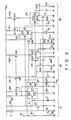
- Fig. 3 showing a burst gate pulse generating circuit according to an embodiment of the present invention.
- the base of an npn transistor Q1 is coupled through a resistor R1 with an input terminal IN that is coupled for reception with a sync separation signal.
- the same base is also connected through a resistor R2 to a ground potential V SS .
- the emitter of the transistor Q1 is connected to the ground potential V SS , and the collector thereof is connected to a power source potential V CC through a constant current source I1.
- the same collector is further connected to the base of an npn transistor Q2.
- the transistor Q2 is connected at the emitter to the ground potential V SS , and at the collector to the power source potential V CC via a resistor R3.
- the collector of the transistor Q2 is further connected to the ground potential V SS via a capacitor C1, and to the base of an npn transistor Q3.
- These transistors Q1 and Q2, resistors R1 to R3, a capacitor C1 and constant current source I1 make up a first circuit 10.
- the collector of the transistor Q3 is coupled with the power source potential V CC via a resistor R4, and the emitter thereof is connected to the ground potential V SS via a resistor R5.
- the emitter of the same transistor is also connected to the emitter of an npn transistor Q4.
- the transistors Q3 and Q4 whose emitters are interconnected make up a first differential amplifier A1.
- the base of the transistor Q4 is connected through a resistor R6 to the ground potential V SS , and through a resistor R7 to the collector of the transistor Q3.
- the collector of the transistor Q4 is connected to the collector and the base of a pnp transistor Q5.
- the emitter of the transistor Q5 is connected through a resistor R8 to the power source potential V CC .
- the base of the transistor Q5 is connected to the base of a pnp transistor Q6.
- the emitter of the transistor Q6 is connected through a resistor R9 to the power source potential V CC , and the collector thereof is connected through a resistor R10 to the ground potential V SS and to the base of the transistor Q7.
- the emitter of the transistor Q7 is coupled with the ground potential V SS , and the collector thereof is connected to the base of an npn transistor Q8.
- the emitter of the transistor Q8 is coupled with the ground potential V SS , and the collector thereof is connected to the base of the transistor Q4.
- the collector of the transistor Q2 is connected to the base of an npn transistor Q9.
- the collector of the transistor Q9 is connected to the power source potential V CC , and the emitter thereof is connected to the emitter of an npn transistor Q10.
- the transistor Q9 and the transistor Q10 whose emitters are interconnected make up a second differential amplifier A2.
- the emitters of these transistors Q9 and Q10 are connected through a constant current source I2 to the ground potential V SS .
- the base of the transistor Q10 is connected to the ground potential V SS via a constant voltage source V2.
- the collector of the transistor Q10 is connected to the collector and the base of a pnp transistor Q11.
- the emitter of the transistor Q11 is connected through a resistor R11 to the power source potential V CC .
- the base of the transistor Q11 is connected to the base of a pnp transistor Q12.
- the emitter of the transistor Q12 is connected to the power source potential V CC by way of a resistor R12.
- the collector thereof is connected to the collectors of transistors Q13 and Q14 of the pnp type.
- the transistors Q13 and Q14 cooperate to form a third differential amplifier A3.
- the base of the transistor Q13 is connected to the collector of the transistor Q2, and collector thereof is coupled with the ground potential V SS .
- the base of the transistor Q14 is connected through a constant voltage source V1 to the ground potential V SS .
- the collector of the transistor Q14 is connected to the collector of an npn transistor Q15, and an output terminal OUT from which a stream of a burst gate pulse is produced.
- the collector of the transistor Q14 is connected through a resistor R13 to the ground potential V SS .
- the emitter of the transistor Q15 is connected to the ground potential V SS , and its base is connected to the collector of the transistor Q1.
- the base of an npn transistor Q16 is connected to the input terminal IN, and its collector is connected to the power source potential V CC .
- the emitter of the transistor Q16 is connected to the emitters of the transistors Q9 and Q10 that are connected together.
- Base of an npn transistor Q17 is connected through a resistor R16 to the input terminal IN.
- the emitter of this transistor Q17 is connected through a resistor R17 to the ground potential V SS , and its collector is connected to the base of an npn transistor Q18 and the collector of a pnp transistor Q19.
- the collector of the transistor Q17 is connected to the ground potential V SS via a resistor R14.
- the collector of the transistor Q18 is connected to the base of the transistor Q7, and its emitter is connected to the ground potential V SS .
- the base of the transistor Q19 is connected to the collector of the transistor Q2, and its emitter is connected to the emitter of a pnp transistor Q20.
- the transistors Q19 and Q20 that are interconnected at the emitters make up a fourth differential amplifier A4.
- the collector of the transistor Q20 is connected to the ground potential V SS , and its base is connected through a constant voltage source V3 to the ground potential V SS .
- the emitters of the transistors Q19 and Q20 are connected together and to the collector of a pnp transistor Q21.
- the transistors Q21 and Q5 are interconnected at the bases.
- the emitter of the transistor Q21 is connected through a resistor R15 to the power source potential V CC .
- the differential amplifiers A1 and A4, transistors Q5 to Q8, Q17 to Q20, resistors R4 to R10, R14 to R17, and constant voltage source V3 cooperate to form a second circuit 20.
- the differential amplifiers A2 and A3, transistors Q11, Q12 and Q15, resistors R11, R12 and R13, constant voltage sources V1 and V2, and constant current source I2 cooperate to form a third circuit 30.
- a voltage of the constant current source V3 is smaller than those of the constant voltage source V1 and V2.
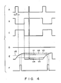
- Fig. 4 shows a timing chart useful in explaining the operation of the bust gate pulse generating circuit shown in Fig. 3.
- a waveform A represents a variation of a sync separation signal applied to the input terminal IN;
- a waveform B a voltage variation of a base signal of each of the transistors Q2, Q8 and Q15;
- a waveform C a voltage variation of a base signal each of the transistors Q4 and Q7 or a current variation at the collector terminal of each of the transistors Q5 and Q6;
- a waveform D a voltage variation of a base signal of the transistor Q18;
- a waveform E a variation of a base voltage of the transistor Q3;
- a waveform E a voltage variation of a signal derived from the output terminal OUT.
- the transistor Q1 is turned off, the transistors Q2 and Q8 are turned on, and the transistors Q3, Q4, Q5, Q6 and Q7 are turned off.
- the transistors Q16 and Q9 are turned off, the transistors Q10, Q11, Q12, Q13 are turned on, and the transistors Q14 and Q15 are turned off. Accordingly, the signal at the output terminal OUT becomes "0" in level, as indicated by the waveform F in Fig. 4.
- the transistor Q1 is turned off, the transistors Q4, Q5, Q6, and Q7 are turned on, and the transistors Q2 and Q8 are turned off.
- the power source potential V CC starts to charge the capacitor C1 through the resistor R3.
- the transistor Q3 is turned on, so that the transistors Q4 to Q7 are turned off. Then, the transistor Q2 and Q8 are turned on. This state is the same as that in the first mode. Also in the second state, the signal at the output terminal OUT becomes "0" in level as indicated by the waveform F in Fig. 4.
- the transistor Q1 When the sync separation signal rises to "1" level, the transistor Q1 is turned on. The transistors Q2, Q8 and Q15 are cut off. At this time, the base voltage of the transistor Q4 is set to V0 and transistor Q2 is turned off, so that charge to the capacitor C1 starts through the resistor R3 at a time constant as defined by the values of the capacitor C1 and the resistor R3. The base voltage of the transistor Q3 rises as indicated by the waveform E. Until the base voltage exceeds the voltage V0, the transistor Q3 remains cut off, while the transistor Q4 remains turned on. The result is that the transistors Q5, Q6, and Q7 are in an on state and the transistors Q2, Q8 and Q15 are left in an off state.
- the transistor Q1 When the sync separation signal is pulsed from “1" to “0, the transistor Q1 is turned off. At this time, the transistors Q4, Q5, Q6, and Q7 maintain an on state, while the transistors Q2, Q8 and Q15 maintain a cut-off state. The transistors Q10 to Q13 are in an on state. The charge to the capacitor C1 is performed. When the base voltage of the transistor Q13 exceeds the constant voltage V1, the transistor Q14 is turned on and the voltage at the output terminal OUT rises to "1" as indicated by the waveform F in Fig. 4. The charge to the capacitor C1 is succeedingly performed, and the transistor Q10 is cut off.
- the transistors Q11 and Q12 are cut off, and the current supply to the transistors Q13 and Q14 is stopped.
- the transistor Q14 is cut off, and the signal at the output terminal OUT drops from "1" to "0". See the waveform F in Fig. 4.
- the transistor Q3 When the base voltage of the transistor Q3 exceeds the voltage V0, the transistor Q3 is turned on, the transistor Q4 is cut off, and the transistors Q5, Q6 and Q7 are cut off. As the result of turning on the transistor Q3, the capacitor C1 thus far being charged is discharged through the transistor Q3 to the ground potential V SS . The base voltage of the transistor Q3 is immediately placed at the potential V SS . See the waveform E in Fig. 4. Under this condition, the transistor Q1 is cut off, while the transistors Q2, Q8 and Q15 are turned on.
- a burst gate pulse of a fixed pulse width appears at a position delayed by a predetermined time behind the normal sync pulse.
- the voltage value of the constant voltage source V3 must be smaller than the voltage V5 (see the waveform E) that is obtained when the capacitor C1 is charged by the power source potential V CC prior to a period T before a normal sync separation pulse arrives at the input terminal INPUT.
- the period T is equal to the pulse of the input sync separation pulse.
Landscapes
- Engineering & Computer Science (AREA)
- Multimedia (AREA)
- Signal Processing (AREA)
- Processing Of Color Television Signals (AREA)
- Synchronizing For Television (AREA)
- Electronic Switches (AREA)
- Devices For Checking Fares Or Tickets At Control Points (AREA)
Applications Claiming Priority (2)
| Application Number | Priority Date | Filing Date | Title |
|---|---|---|---|
| JP63161342A JPH0720250B2 (ja) | 1988-06-29 | 1988-06-29 | バーストゲートパルス生成回路 |
| JP161342/88 | 1988-06-29 |
Publications (3)
| Publication Number | Publication Date |
|---|---|
| EP0348966A2 true EP0348966A2 (de) | 1990-01-03 |
| EP0348966A3 EP0348966A3 (en) | 1990-02-28 |
| EP0348966B1 EP0348966B1 (de) | 1992-12-16 |
Family
ID=15733259
Family Applications (1)
| Application Number | Title | Priority Date | Filing Date |
|---|---|---|---|
| EP89111828A Expired - Lifetime EP0348966B1 (de) | 1988-06-29 | 1989-06-29 | Burst-Torimpulserzeugungsschaltung |
Country Status (5)
| Country | Link |
|---|---|
| US (1) | US5038203A (de) |
| EP (1) | EP0348966B1 (de) |
| JP (1) | JPH0720250B2 (de) |
| KR (1) | KR920004332B1 (de) |
| DE (1) | DE68903890T2 (de) |
Families Citing this family (4)
| Publication number | Priority date | Publication date | Assignee | Title |
|---|---|---|---|---|
| US5231509A (en) * | 1989-11-27 | 1993-07-27 | Matsushita Electric Industrial Co., Ltd. | Burst gate pulse generating device for use in image signal reproducing system |
| US5258091A (en) * | 1990-09-18 | 1993-11-02 | Sumitomo Electric Industries, Ltd. | Method of producing X-ray window |
| JP2925767B2 (ja) * | 1991-02-26 | 1999-07-28 | ローム株式会社 | 信号ライン切り換え回路 |
| US7726746B2 (en) * | 2007-08-28 | 2010-06-01 | Berens Martin C | Hubcap having lighted spinning element |
Family Cites Families (5)
| Publication number | Priority date | Publication date | Assignee | Title |
|---|---|---|---|---|
| ES374096A1 (es) * | 1968-11-21 | 1971-12-01 | Zenith Radio Corp | Mejoras en las redes de traslacion de senales. |
| US3949418A (en) * | 1975-01-27 | 1976-04-06 | Gte Sylvania Incorporated | Burst gate and backporch clamping circuitry |
| US4228456A (en) * | 1979-06-20 | 1980-10-14 | Gte Products Corporation | Burst gating signal generating circuit |
| US4410907A (en) * | 1981-11-16 | 1983-10-18 | Rca Corporation | Burst gate keying and back porch clamp pulse generator |
| US4581630A (en) * | 1983-08-30 | 1986-04-08 | Rca Corporation | Constant width burst gate keying pulse generator |
-
1988
- 1988-06-29 JP JP63161342A patent/JPH0720250B2/ja not_active Expired - Fee Related
-
1989
- 1989-06-26 US US07/371,001 patent/US5038203A/en not_active Expired - Lifetime
- 1989-06-29 KR KR1019890009114A patent/KR920004332B1/ko not_active Expired
- 1989-06-29 EP EP89111828A patent/EP0348966B1/de not_active Expired - Lifetime
- 1989-06-29 DE DE8989111828T patent/DE68903890T2/de not_active Expired - Fee Related
Also Published As
| Publication number | Publication date |
|---|---|
| DE68903890T2 (de) | 1993-05-13 |
| EP0348966B1 (de) | 1992-12-16 |
| JPH0720250B2 (ja) | 1995-03-06 |
| KR900001126A (ko) | 1990-01-31 |
| EP0348966A3 (en) | 1990-02-28 |
| KR920004332B1 (ko) | 1992-06-01 |
| JPH0211086A (ja) | 1990-01-16 |
| DE68903890D1 (de) | 1993-01-28 |
| US5038203A (en) | 1991-08-06 |
Similar Documents
| Publication | Publication Date | Title |
|---|---|---|
| EP0348966A2 (de) | Burst-Torimpulserzeugungsschaltung | |
| EP0058729B1 (de) | Synchronsignal trennschaltung | |
| US3809808A (en) | Video sync separator | |
| US3510578A (en) | Television camera power supply | |
| US4812907A (en) | Sync pulse separator system | |
| US4324990A (en) | Comparison circuit adaptable for utilization in a television receiver or the like | |
| US4446483A (en) | Circuit arrangement for deriving a field synchronizing signal from an incoming signal | |
| US4384305A (en) | Circuit arrangement for generating a synchronizable sawtooth voltage | |
| US3943385A (en) | Time switch circuit having a switch-back time delay | |
| EP0107205B1 (de) | Torimpuls-Erzeugungsschaltung und Farbfernsehempfänger | |
| EP0339718A2 (de) | Vorrichtung zur Verarbeitung eines Videosignals | |
| JPS6129188B2 (de) | ||
| JP2815865B2 (ja) | 同期信号分離回路 | |
| JPH099104A (ja) | ソフトクランプ装置及びソフトクランプ方法 | |
| GB1267979A (en) | Synchronizing separator circuits | |
| JPH023586B2 (de) | ||
| JPS596676A (ja) | 情報信号插入回路 | |
| JPS5851720B2 (ja) | Virキラ−信号発生回路 | |
| KR870000835B1 (ko) | 잡음신호에 대한 무방송채널 잡음제거회로 | |
| CA1208760A (en) | Vertical interval data blanker | |
| JPS6034093Y2 (ja) | テ−プレコ−ダの録音切換え回路 | |
| KR900006815Y1 (ko) | Vcr의 영상출력시 멜로디 자동 차단회로 | |
| JPH06318842A (ja) | 遅延フィルタ | |
| EP0040275A1 (de) | Komparatorschaltung zur Verwendung in einem Fernsehempfänger oder dgl. | |
| JPS6219106B2 (de) |
Legal Events
| Date | Code | Title | Description |
|---|---|---|---|
| PUAI | Public reference made under article 153(3) epc to a published international application that has entered the european phase |
Free format text: ORIGINAL CODE: 0009012 |
|
| 17P | Request for examination filed |
Effective date: 19890629 |
|
| AK | Designated contracting states |
Kind code of ref document: A2 Designated state(s): DE FR GB |
|
| PUAL | Search report despatched |
Free format text: ORIGINAL CODE: 0009013 |
|
| AK | Designated contracting states |
Kind code of ref document: A3 Designated state(s): DE FR GB |
|
| 17Q | First examination report despatched |
Effective date: 19920303 |
|
| GRAA | (expected) grant |
Free format text: ORIGINAL CODE: 0009210 |
|
| AK | Designated contracting states |
Kind code of ref document: B1 Designated state(s): DE FR GB |
|
| REF | Corresponds to: |
Ref document number: 68903890 Country of ref document: DE Date of ref document: 19930128 |
|
| ET | Fr: translation filed | ||
| REG | Reference to a national code |
Ref country code: FR Ref legal event code: CD |
|
| PLBE | No opposition filed within time limit |
Free format text: ORIGINAL CODE: 0009261 |
|
| STAA | Information on the status of an ep patent application or granted ep patent |
Free format text: STATUS: NO OPPOSITION FILED WITHIN TIME LIMIT |
|
| 26N | No opposition filed | ||
| PGFP | Annual fee paid to national office [announced via postgrant information from national office to epo] |
Ref country code: FR Payment date: 19970610 Year of fee payment: 9 |
|
| PGFP | Annual fee paid to national office [announced via postgrant information from national office to epo] |
Ref country code: GB Payment date: 19970620 Year of fee payment: 9 |
|
| PGFP | Annual fee paid to national office [announced via postgrant information from national office to epo] |
Ref country code: DE Payment date: 19970704 Year of fee payment: 9 |
|
| PG25 | Lapsed in a contracting state [announced via postgrant information from national office to epo] |
Ref country code: GB Free format text: LAPSE BECAUSE OF NON-PAYMENT OF DUE FEES Effective date: 19980629 |
|
| GBPC | Gb: european patent ceased through non-payment of renewal fee |
Effective date: 19980629 |
|
| PG25 | Lapsed in a contracting state [announced via postgrant information from national office to epo] |
Ref country code: FR Free format text: LAPSE BECAUSE OF NON-PAYMENT OF DUE FEES Effective date: 19990226 |
|
| PG25 | Lapsed in a contracting state [announced via postgrant information from national office to epo] |
Ref country code: DE Free format text: LAPSE BECAUSE OF NON-PAYMENT OF DUE FEES Effective date: 19990401 |
|
| REG | Reference to a national code |
Ref country code: FR Ref legal event code: ST |