EP0348230A2 - Verfahren zur Herstellung eines Dünnfilmmagnetkopfes - Google Patents
Verfahren zur Herstellung eines Dünnfilmmagnetkopfes Download PDFInfo
- Publication number
- EP0348230A2 EP0348230A2 EP89306405A EP89306405A EP0348230A2 EP 0348230 A2 EP0348230 A2 EP 0348230A2 EP 89306405 A EP89306405 A EP 89306405A EP 89306405 A EP89306405 A EP 89306405A EP 0348230 A2 EP0348230 A2 EP 0348230A2
- Authority
- EP
- European Patent Office
- Prior art keywords
- layer
- resin film
- magnetic
- core layer
- thickness
- Prior art date
- Legal status (The legal status is an assumption and is not a legal conclusion. Google has not performed a legal analysis and makes no representation as to the accuracy of the status listed.)
- Granted
Links
Images


Classifications
-
- H—ELECTRICITY
- H01—ELECTRIC ELEMENTS
- H01F—MAGNETS; INDUCTANCES; TRANSFORMERS; SELECTION OF MATERIALS FOR THEIR MAGNETIC PROPERTIES
- H01F41/00—Apparatus or processes specially adapted for manufacturing or assembling magnets, inductances or transformers; Apparatus or processes specially adapted for manufacturing materials characterised by their magnetic properties
- H01F41/32—Apparatus or processes specially adapted for manufacturing or assembling magnets, inductances or transformers; Apparatus or processes specially adapted for manufacturing materials characterised by their magnetic properties for applying conductive, insulating or magnetic material on a magnetic film, specially adapted for a thin magnetic film
- H01F41/34—Apparatus or processes specially adapted for manufacturing or assembling magnets, inductances or transformers; Apparatus or processes specially adapted for manufacturing materials characterised by their magnetic properties for applying conductive, insulating or magnetic material on a magnetic film, specially adapted for a thin magnetic film in patterns, e.g. by lithography
-
- G—PHYSICS
- G11—INFORMATION STORAGE
- G11B—INFORMATION STORAGE BASED ON RELATIVE MOVEMENT BETWEEN RECORD CARRIER AND TRANSDUCER
- G11B5/00—Recording by magnetisation or demagnetisation of a record carrier; Reproducing by magnetic means; Record carriers therefor
- G11B5/127—Structure or manufacture of heads, e.g. inductive
- G11B5/31—Structure or manufacture of heads, e.g. inductive using thin films
- G11B5/3163—Fabrication methods or processes specially adapted for a particular head structure, e.g. using base layers for electroplating, using functional layers for masking, using energy or particle beams for shaping the structure or modifying the properties of the basic layers
-
- Y—GENERAL TAGGING OF NEW TECHNOLOGICAL DEVELOPMENTS; GENERAL TAGGING OF CROSS-SECTIONAL TECHNOLOGIES SPANNING OVER SEVERAL SECTIONS OF THE IPC; TECHNICAL SUBJECTS COVERED BY FORMER USPC CROSS-REFERENCE ART COLLECTIONS [XRACs] AND DIGESTS
- Y10—TECHNICAL SUBJECTS COVERED BY FORMER USPC
- Y10T—TECHNICAL SUBJECTS COVERED BY FORMER US CLASSIFICATION
- Y10T29/00—Metal working
- Y10T29/49—Method of mechanical manufacture
- Y10T29/49002—Electrical device making
- Y10T29/4902—Electromagnet, transformer or inductor
- Y10T29/49021—Magnetic recording reproducing transducer [e.g., tape head, core, etc.]
- Y10T29/49032—Fabricating head structure or component thereof
- Y10T29/49036—Fabricating head structure or component thereof including measuring or testing
- Y10T29/49043—Depositing magnetic layer or coating
- Y10T29/49044—Plural magnetic deposition layers
-
- Y—GENERAL TAGGING OF NEW TECHNOLOGICAL DEVELOPMENTS; GENERAL TAGGING OF CROSS-SECTIONAL TECHNOLOGIES SPANNING OVER SEVERAL SECTIONS OF THE IPC; TECHNICAL SUBJECTS COVERED BY FORMER USPC CROSS-REFERENCE ART COLLECTIONS [XRACs] AND DIGESTS
- Y10—TECHNICAL SUBJECTS COVERED BY FORMER USPC
- Y10T—TECHNICAL SUBJECTS COVERED BY FORMER US CLASSIFICATION
- Y10T29/00—Metal working
- Y10T29/49—Method of mechanical manufacture
- Y10T29/49002—Electrical device making
- Y10T29/4902—Electromagnet, transformer or inductor
- Y10T29/49021—Magnetic recording reproducing transducer [e.g., tape head, core, etc.]
- Y10T29/49032—Fabricating head structure or component thereof
- Y10T29/49036—Fabricating head structure or component thereof including measuring or testing
- Y10T29/49043—Depositing magnetic layer or coating
- Y10T29/49046—Depositing magnetic layer or coating with etching or machining of magnetic material
-
- Y—GENERAL TAGGING OF NEW TECHNOLOGICAL DEVELOPMENTS; GENERAL TAGGING OF CROSS-SECTIONAL TECHNOLOGIES SPANNING OVER SEVERAL SECTIONS OF THE IPC; TECHNICAL SUBJECTS COVERED BY FORMER USPC CROSS-REFERENCE ART COLLECTIONS [XRACs] AND DIGESTS
- Y10—TECHNICAL SUBJECTS COVERED BY FORMER USPC
- Y10T—TECHNICAL SUBJECTS COVERED BY FORMER US CLASSIFICATION
- Y10T29/00—Metal working
- Y10T29/49—Method of mechanical manufacture
- Y10T29/49002—Electrical device making
- Y10T29/4902—Electromagnet, transformer or inductor
- Y10T29/49021—Magnetic recording reproducing transducer [e.g., tape head, core, etc.]
- Y10T29/49032—Fabricating head structure or component thereof
- Y10T29/4906—Providing winding
- Y10T29/49064—Providing winding by coating
Definitions
- the present invention relates to a process for producing thin film magnetic heads. More particularly the invention relates to a process for producing a thin film magnetic head for use in writing data on or reading data from magnetic recording media such as magnetic tapes or magnetic discs, the head being suited especially to high-density recording.
- Thin film magnetic heads have the features of being small-sized, assuring facilitated recording of data with a high density in a multiplicity of channels and being adapted to form tracks of more accurate and reduced width. They are small in inductance, low in core loss and therefore excellent in radio-frequency characteristics, and have the ability for recording with high resolution because they produce a sharp magnetic field distribution. In addition to these features in characteristics, these magnetic heads are amenable to mass production at a greatly reduced cost. With the requirement for high-density magnetic recording in recent years, thin film magnetic heads have proved remarkably superior because of these features, and active research and development efforts have been made in this field (U.S.P. No. 4,677,036, etc.).
- a substrate 1 has formed thereon a lower magnetic core layer 2.
- the substrate 1 is made of a material having high wear resistance, such as ferrite, alumina or glass.
- the lower magnetic core layer 2 is in the form of a film of a soft magnetic metal such as Ni-Fe, Fe-Al-Si or Co-based amorphous alloys and provides one of a pair of cores of the magnetic head.
- An upper magnetic core layer 3 is formed over the lower core layer 2. Like the lower layer 2, the upper core layer 3 is made of a soft magnetic metal film and serves as the other core of the magnetic head.
- an insulating layer 4 Provided between the upper core layer 3 and the lower core layer 2 is an insulating layer 4 forming a thin magnetic gap 5 at the tip of the head and having an electrically conductive coil layer 6 embedded therein.
- the conductive coil 6 is in the form of a spiral coil extending continuously rightward in Fig. 3 and shown in section of its one side.
- the two core layers 2, 3 are joined together at the portion C illustrated.
- the conductive coil layer 6 is made of a film of a conductor such as Cu, Al, Au or Ag.
- the insulating layer 4 is made of a film of a nonmagnetic material such as SiO2, Al2O3 or Si3N4.
- the thin film magnetic head is fabricated by forming over the substrate 1 the lower magnetic core layer 2 and the insulating layer 4 having a specified shape and embedding the conductive coil 6 as shown in Fig. 3 (b), thereafter forming in a vapor phase the upper magnetic core layer 3 in a predetermined pattern over an area ⁇ to cover the magnetic gap 5 and the joint portion C (Fig. 3 (c)), and removing the tip of the resulting assembly over a predetermined length ⁇ by grinding.
- the upper magnetic core layer 3 is formed in the predetermined pattern conventionally by the wet etching method, ion milling method or lift-off method.
- the upper core layer 3 is masked with a photoresist film and then etched in the predetermined pattern with an etching solution.
- This method has the advantage that the layer can be etched in a short period of time without the necessity of using an expensive apparatus.
- the ion etching method is a physical etching method wherein the impact of Ar ion or like inactive ion is used in stead of the etching solution.
- the lift-off method forms the upper magnetic core layer 3 in the predetermined pattern without etching.
- Fig. 4 shows a case wherein the upper magnetic core layer 3 is formed directly on a substrate.
- a photoresist film 12 is first formed on the substrate and then etched in a specified pattern, which is reverse to the pattern of the core layer 3 to be formed. Subsequently, an upper magnetic material layer 13 is formed over the entire upper surface obtained to provide the upper magnetic core layer 3 later. As seen in Fig. 4 (a), therefore, the portion of the magnetic material layer 13 corresponding to the pattern of the upper core layer 3 to be formed is formed directly on the substrate 11, with the other unnecessary portion thereof formed on the photoresist film 12.
- the substrate 11 is then immersed in its entirety in acetone or like organic solvent, whereupon the organic solvent penetrates through the clearances (indicated by arrows A shown) between the magnetic material layer 13 on the substrate 11 and the magnetic material layer 13 on the photoresist film 12 to dissolve the photoresist film 12.
- the magnetic material layer 13 over the film 12 is separated off, with the result that the remaining portion of the upper magnetic material layer 13 provides the upper magnetic core layer 3 in the predetermined pattern as shown in Fig. 4 (b).
- the upper magnetic core layer 3 which was about 1 to about 5 ⁇ m in thickness, is made as thick as about 10 to about 30 ⁇ m and thereby prevented from magnetic saturation.
- the ion milling method does not permit selective etching for the upper magnetic core layer 3 because of its nature as a physical etching method, and the photoresist film serving as a mask and the insulating layer 4 are always etched with the core layer 3.
- the core layer 3 is slightly overetched so as to cancel any influence by variations in the thickness in the layer 3 and in the etching rate from portion to portion.
- the degree of overetching poses no problem when the core layer is several micrometers in thickness but produces an unnegligible influence if the thickness is as large as 10 to 30 ⁇ m. More specifically, it is likely that the etching is continued even after the core layer 3 has been etched through the entire thickness thereof, possibly removing the insulating layer 4 to result in objections such as exposure of or damage to the conductive coil layer 6 and a break in this layer 6.
- the lift-off method is free of the above drawbacks since the upper magnetic material layer 13 is not etched in this method.
- the photoresist film formed be eventually removable by dissolving with an organic solvent, whereas when subjected to a high temperature, the photoresist film is liable to change into a film which is sparingly soluble with the organic solvent. Accordingly, if the photoresist film formed is heated to a high temperature (for example, of not lower than 150 o C), the film becomes unremovable or less-removable by dissolving in the final step.
- the substrate temperature must be lower than usually (e.g. lower than 100°C), but the lower substrate temperature reduces the adhesion of the magnetic core layer to the underlying layer and entails impaired magnetic characteristics.
- photoresist films as formed are inherently sparingly soluble with a conventional organic solvent and are not suitable for the lift-off method.
- the present invention has been accomplished in view of the foregoing situation, especially to overcome the problems involved in the fabrication of thin film magnetic heads utilizing the lift-off method.
- the present invention provides a process for producing a thin film magnetic head comprising forming a nonmagnetic material layer over a lower magnetic core layer with an electrically conductive coil layer incorporated in the nonmagnetic material layer, and forming an upper magnetic core layer of a predetermined pattern over the resultant to provide the thin film magnetic head, the upper magnetic core layer of the predetermined pattern being formed by the steps of:
- the pattern of the upper magnetic core layer is formed by the lift-off method.
- the most distinct feature of the present process is that in the lift-off method, the resin film is removed by plasma etching.
- the present invention has been accomplished based on the finding that the resin film, even if sparingly soluble with organic solvents, can be efficiently removed by plasma etching in the manner of side etching, thereby permitting vapor-phase formation of the upper magnetic core layer at a high temperature and consequently enabling this core layer to exhibit excellent magnetic characteristics.
- the process of the invention therefore has the following advantages.
- the lower magnetic core layer is formed usually on a substrate of a nonmagnetic or magnetic material having high wear resistance, such as ferrite, alumina or glass.
- the lower magnetic core layer is prepared preferably from a soft magnetic metal such as Ni-Fe, Fe-Al-Si or like iron alloy or cobalt amorphous alloy by a known method such as electroplating, vacuum evaporation, sputtering or the like.
- the substrate of a magnetic material can be used as a combined substrate and lower magnetic core layer.
- the conductive coil layer is made preferably of a conductive metal such as Cu, Al, Au or Ag.
- the nonmagnetic material layer having the conductive coil layer embedded therein and providing a magnetic gas at the tip of the head and a magnetic head connecting opening is prepared preferably from an insulating material such as SiO2, Al2O3 or Si3N4.
- the conductive coil layer and the nonmagnetic material layer can be formed and patterned by known method.
- the upper magnetic core layer is formed over the nonmagnetic material layer by the foregoing steps (a) to (d).
- a resin film is formed.
- the material to be used for forming the resin film is one which will not decompose or melt during the step of forming the magnetic material layer to be described later.
- suitable materials are resins amenable to thermal sintering processes, such as polyimide resins and polyimido-siloxane resins, photosensitive resins for use in the electronics industry, UV resists, Deep-UV resists, resins curable with electron beams or X-rays etc.
- examples of useful polyimide or polyimido-siloxane resins are PIQ or PIX series (products of Hitachi Chemical Co., Ltd., Japan), Du Pont PYRALIN series and SP series (Toray Industries, Inc., Japan).
- Examples of useful photosensitive resins are PIL series (Hitachi Chemical Co., Ltd.)
- Examples of useful UV resists, etc. are Hoechst AZ series, OMR series (Tokyo Ohyokagaku Co., Ltd., Japan), Hunt Chemical Waycoat series and the like.
- the thickness of the resin film is suitably about a half to 2 times thickness of the upper magnetic core layer to be formed.
- the thickness is suitably 5 to 50 ⁇ m, preferably 10 to 30 ⁇ m, in view of the plasma etching rate.
- the resin film need not always be cured or sintered, or may be cured or sintered to such an extent that it becomes insoluble with organic solvents.
- the film can be formed by a known method such as coating, dipping or spinner method.
- step (b) the resin film is patterned.
- the pattern is reverse to the pattern of the upper magnetic core layer to be formed.
- the film can be patterned by forming or applying a specified mask.
- a magnetic material layer is formed over the resin film pattern. It is suitable to prepare the magnetic material layer from a soft magnetic metal, such as Ni-Fe, Fe-Al-Si or cobalt-based amorphous alloy, already mentioned.
- the layer can be formed by a known method such as electroplating, vacuum evaporation or sputtering.
- the thickness of the layer which is not limited specifically, can be about 5 to about 50 ⁇ m, preferably about 10 to about 30 ⁇ m.
- the area over which the magnetic material layer is to be formed needs to be such that the layer at least entirely covers the pattern of the upper magnetic core layer to be formed, and may be part of the resin film formed area.
- the magnetic material layer may be formed over the required areas only.
- the upper surface of the resin film may be entirely covered with the magnetic material layer first, and the undersired portions may then be etched away. The magnetic material layer thus formed completely covers each opening in the resin film pattern which defines the pattern of the upper magnetic core layer and leaves the resin film locally exposed without completely covering the entire upper surface of the resin film.
- the substrate bearing the magnetic material layer thus formed is subjected to plasma etching in step (d).
- the plasma etching step is performed in an atmosphere of oxygen-containing gas.
- oxygen-containing gases are pure O2 gas, 10% N2-O2 gas and the like.
- the gas may contain H2O, H2, CH4 and the like. CF4, C2F6 and the like may also be present in the gas.
- the gas pressure be 0.1 to several torr, and that the power for the glow discharge be usually 200 to 400 W.
- the resin film beneath the magnetic material layer is etched away by the plasma etching step in the manner of side etching through the clearance between the magentic material layer and the resin film and through the exposed side portions of the resin film. Consequently, only the portion of the magnetic material layer on the resin film is removed to completely form an upper magnetic core layer in the predetermined pattern.
- the thin film magnetic head thus obtained has its tip ground as seen in Fig. 3 before use.
- the embodiment will be described as a process for producing thin film magnetic heads including a coil and having the construction shown in Fig. 3 and already described.
- a lower magnetic core layer 2 is formed over the entire upper surface of a substrate as seen in Fig. 1 (a).
- the core layer 2 is an Fe-Al-Si film having a thickness of 3 ⁇ m and formed by sputtering method (at a substrate tempera ture of 250°C).
- the substrate is made of Mn-Zn Ferrite.
- an insulating layer 4 and a conductive coil layer 6 are formed, each in a specified pattern and with a specified thickness, over the lower magnetic core layer 2. More specifically, a lower layer portion of the insulating layer 4 is formed over the entire surface of the core layer 2, the coil layer 6 is formed in a spiral pattern as specified on the layer portion, and an upper layer portion of the insulating layer 4 is formed over the entire upper surface obtained.
- the coil layer 6 is shown in vertical section of its one side only.
- the insulating layer 4 is partially etched away by a taper etching method, i.e., reactive ion etching (RIE).
- RIE reactive ion etching
- a thin insulating layer is formed again for providing a magnetic gap 5 as shown in Fig. 1 (a).
- These insulating layers are each in the form of an SiO2 film formed by plasma CVD.
- the layer 4 is 4 ⁇ m in thickness, and the magnetic gap is 0.3 ⁇ m.
- the conductive coil 6 comprises a Cu film formed by vacuum evaporation.
- the resin film 7 comprises a polyimide (PIQ 3200, Hitachi Chemical Co., Ltd.) film having a thickness of about 15 ⁇ m and formed by coating and baking at 300 to 400°C.
- the resin film 7 may be a photoresist film which is baked at a temperature higher than is usual, i.e., at least 150 to at least 200°C.
- the preferred thickness of the resin film 7 can be determined suitably according to the thickness of the upper magnetic material layer 8 to be formed later, the condition for the subsequent plasma etching, etc.
- the resin film 7 can be formed also by the so-called positive-negative process, i.e., by locally removing a polyimide film with a resist developer.
- the polyimide film thus formed is made of a precusor for polyimide resin since it has not been baked.
- a photosensitive polyimide resist is also usable.
- the method of forming the film 7 is not limited specifically.
- the resin film 7 is etched to a specified pattern as seen in Fig. 1 (c) by forming a mask in the specified pattern from a material resistant to oxygen plasma, such as Cu, Al or SiO2 (Cu is used in the present case) and resorting to reactive ion etching with use of oxygen gas.
- the pattern of the resin film 7 is reverse to the pattern of the upper magnetic core layer 3 to be formed later. Accordingly, the resin film 7 leaves exposed the portion where the core layer 3 is to be formed. Thc mask used for etching the resin film 7 is thereafter removed.
- an upper magnetic material layer 8 is formed over the specified area of the resulting upper surface as seen in Fig. 1 (d).
- the layer 8 provides an upper magnetic core layer 3 later and comprises an Fe-Al-Si film having a thickness of about 15 ⁇ m.
- the layer 8 is formed by sputtering method at a substrate temperature of about 250°C.
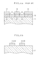
- Fig. 2 is a plan view showing the area where the upper magnetic material layer 8 is formed for mass production.
- Indicated at E, E, ... in the drawing are areas where the upper magnetic core layer is to be formed for thin film magnetic heads individually and each of which corresponds to the aforementioned opening in the resin film.
- the hatched portion D represents the area where the magnetic material layer 8 is formed.
- l1 100 ⁇ m
- l2 100 ⁇ m.
- l1 is usually 100 to 500 ⁇ m
- l2 is usually up to 300 ⁇ m.
- the area D covers all the openings E in the resin film 7 and covers the upper surface of the resin film 7 only partially.
- the pattern of magentic material layer is formed over the area D by forming the layer over the entire upper surface of the resin film and thereafter etching the layer using an HCl-HNO3 etching solution.
- the magnetic material layer 8 can be formed in conformity with the configuration of the specified area D by sputtering or vacuum evaporation with use of a mask but without resorting to etching.
- the portion of the magnetic material layer 8 providing the upper magnetic core layer 3 is formed in the opening E over the lower magnetic core layer 2 and the insulating layer 4, while the unnecessary portion is formed directly on the resin film 7.
- the resin film 7 is removed by plasma etching.
- the plasma etching step is performed using oxygen gas and a hollow cylindrical plasma etching device at an oxygen pressure of 0.8 torr with application of power of 400 W.
- the etching operation is conducted for 10 hours under this condition, the polyimide film is etched away sidewise over a distance of 100 to 150 ⁇ m when having a thickness of 15 ⁇ m, or over a distance of 50 to 100 ⁇ m when having a thickness of 10 ⁇ m.
- the side etching of the resin film 7 can be completed in 10 hours, whereby the unnecessary portion of the upper magnetic material layer 8 over the film 7 can be removed (Fig. 1 (e)).
- the resin film can be etched away sidewise in the direction of arrow F shown in Fig. 2 from one end of the specified area D, so that the etching proceeds at an increased rate, while the amount of etching can be smaller. Further when the plasma etching process is resorted to using such a oxygen-containing reactive gas, the resin layer 7 can be removed completely even if the upper magnetic material layer 8 is formed at an elevated substrate temperature.
- an SiO2 film formed by the plasma CVD process serves as the insulating (nonmagnetic material) layer 4 beneath the resin layer 7 according to the present embodiment
- oxygen gas only is used as the reactive gas for the plasma etching process
- a CF x -O2 reactive gas is used for the plasma etching process
- the resin film 7 can be etched at a further higher rate.
- the thin film magnetic head obtained by removing the unnecessary portion of the magnetic material layer 8 from the upper surface of the resin film 7 in this way has its forward end portion (left end edge shown) to be removed by grinding and is used in the form shown in Fig. 3 for various applications.
Landscapes
- Engineering & Computer Science (AREA)
- Manufacturing & Machinery (AREA)
- Power Engineering (AREA)
- Magnetic Heads (AREA)
Applications Claiming Priority (2)
| Application Number | Priority Date | Filing Date | Title |
|---|---|---|---|
| JP63157267A JP2501873B2 (ja) | 1988-06-23 | 1988-06-23 | 薄膜磁気ヘッドの製造方法 |
| JP157267/88 | 1988-06-23 |
Publications (3)
| Publication Number | Publication Date |
|---|---|
| EP0348230A2 true EP0348230A2 (de) | 1989-12-27 |
| EP0348230A3 EP0348230A3 (de) | 1991-05-02 |
| EP0348230B1 EP0348230B1 (de) | 1995-03-22 |
Family
ID=15645922
Family Applications (1)
| Application Number | Title | Priority Date | Filing Date |
|---|---|---|---|
| EP89306405A Expired - Lifetime EP0348230B1 (de) | 1988-06-23 | 1989-06-23 | Verfahren zur Herstellung eines Dünnfilmmagnetkopfes |
Country Status (4)
| Country | Link |
|---|---|
| US (1) | US4966648A (de) |
| EP (1) | EP0348230B1 (de) |
| JP (1) | JP2501873B2 (de) |
| DE (1) | DE68921795T2 (de) |
Families Citing this family (13)
| Publication number | Priority date | Publication date | Assignee | Title |
|---|---|---|---|---|
| US5236735A (en) * | 1989-05-27 | 1993-08-17 | Tdk Corporation | Method of producing a thin film magnetic head |
| US5256249A (en) * | 1991-09-17 | 1993-10-26 | Seagate Technology, Inc. | Method of manufacturing a planarized magnetoresistive sensor |
| JPH06215329A (ja) * | 1992-11-18 | 1994-08-05 | Mitsumi Electric Co Ltd | 微細導電パターンの形成方法 |
| US6440750B1 (en) | 1997-06-10 | 2002-08-27 | Agere Systems Guardian Corporation | Method of making integrated circuit having a micromagnetic device |
| US6118351A (en) * | 1997-06-10 | 2000-09-12 | Lucent Technologies Inc. | Micromagnetic device for power processing applications and method of manufacture therefor |
| US5966800A (en) * | 1997-07-28 | 1999-10-19 | Read-Rite Corporation | Method of making a magnetic head with aligned pole tips and pole layers formed of high magnetic moment material |
| JP2995170B2 (ja) * | 1998-03-12 | 1999-12-27 | ティーディーケイ株式会社 | 薄膜磁気ヘッドおよびその製造方法 |
| JP3721262B2 (ja) * | 1998-07-23 | 2005-11-30 | 株式会社日立グローバルストレージテクノロジーズ | 薄膜磁気ヘッドの製造方法および磁気ヘッド |
| US6255714B1 (en) | 1999-06-22 | 2001-07-03 | Agere Systems Guardian Corporation | Integrated circuit having a micromagnetic device including a ferromagnetic core and method of manufacture therefor |
| JP2001195708A (ja) * | 2000-01-07 | 2001-07-19 | Tdk Corp | 薄膜磁気ヘッドおよびその製造方法 |
| JP2001344713A (ja) * | 2000-05-29 | 2001-12-14 | Fujitsu Ltd | 薄膜磁気ヘッドの製造方法と薄膜磁気ヘッド |
| CN1910678A (zh) * | 2004-01-19 | 2007-02-07 | 皇家飞利浦电子股份有限公司 | 制造磁光装置的方法 |
| US8070574B2 (en) * | 2007-06-06 | 2011-12-06 | Shuffle Master, Inc. | Apparatus, system, method, and computer-readable medium for casino card handling with multiple hand recall feature |
Family Cites Families (11)
| Publication number | Priority date | Publication date | Assignee | Title |
|---|---|---|---|---|
| US4424271A (en) * | 1982-09-15 | 1984-01-03 | Magnetic Peripherals Inc. | Deposition process |
| JPS59155947A (ja) * | 1983-02-24 | 1984-09-05 | Sumitomo Electric Ind Ltd | 多層配線方法 |
| JPH061769B2 (ja) * | 1983-08-10 | 1994-01-05 | 株式会社日立製作所 | アルミナ膜のパターニング方法 |
| JPS60110140A (ja) * | 1983-11-21 | 1985-06-15 | Hitachi Ltd | 配線構造体形成方法 |
| CA1260754A (en) * | 1983-12-26 | 1989-09-26 | Teiji Majima | Method for forming patterns and apparatus used for carrying out the same |
| JPS6260662A (ja) * | 1985-09-11 | 1987-03-17 | Alps Electric Co Ltd | サ−マルヘツドの製造方法 |
| JPS6284413A (ja) * | 1985-10-09 | 1987-04-17 | Toshiba Corp | 薄膜磁気ヘツドの製造方法 |
| JPS6286517A (ja) * | 1985-10-11 | 1987-04-21 | Seiko Epson Corp | 磁気ヘツドの製造方法 |
| JPS62229513A (ja) * | 1986-03-28 | 1987-10-08 | Nec Kansai Ltd | 薄膜磁気ヘツドの製造方法 |
| JPS62256208A (ja) * | 1986-04-28 | 1987-11-07 | Tdk Corp | 薄膜磁気ヘツドのギヤツプ部の構造 |
| JPS63173213A (ja) * | 1987-01-13 | 1988-07-16 | Hitachi Ltd | 薄膜磁気ヘツドの製造方法 |
-
1988
- 1988-06-23 JP JP63157267A patent/JP2501873B2/ja not_active Expired - Fee Related
-
1989
- 1989-06-23 US US07/370,181 patent/US4966648A/en not_active Expired - Lifetime
- 1989-06-23 DE DE68921795T patent/DE68921795T2/de not_active Expired - Lifetime
- 1989-06-23 EP EP89306405A patent/EP0348230B1/de not_active Expired - Lifetime
Also Published As
| Publication number | Publication date |
|---|---|
| EP0348230A3 (de) | 1991-05-02 |
| US4966648A (en) | 1990-10-30 |
| JP2501873B2 (ja) | 1996-05-29 |
| DE68921795D1 (de) | 1995-04-27 |
| DE68921795T2 (de) | 1995-07-13 |
| EP0348230B1 (de) | 1995-03-22 |
| JPH025213A (ja) | 1990-01-10 |
Similar Documents
| Publication | Publication Date | Title |
|---|---|---|
| EP0430407B1 (de) | Integrierte magnetische Lese-, Schreibekopf-, Biegungsvorrichtungs-, Leiter-Struktur | |
| US5245493A (en) | Magnetic information storage apparatus including magnetic head and method for making magnetic head | |
| EP0348230B1 (de) | Verfahren zur Herstellung eines Dünnfilmmagnetkopfes | |
| US7995307B2 (en) | Perpendicular magnetic recording write head with trailing shield having throat height defined by electroplated nonmagnetic pad layer and method for making the head | |
| US5073242A (en) | Method of making integrated magnetic read/write head/flexure/conductor structure | |
| US20070153418A1 (en) | Magnetic recording head and fabrication process | |
| EP0383739A1 (de) | Verfahren zur Erzeugung eines Dünnfilmmagnetkopfes | |
| US6416936B1 (en) | Top surface imaging technique for top pole tip width control in magnetoresistive read/write head processing | |
| US20020148105A1 (en) | Novel bi-layer lift-off process for high track density GMR head | |
| US6741422B2 (en) | Method of making magnetic head having narrow pole tip and fine pitch coil | |
| JPH08171712A (ja) | 側面露出型薄膜磁気ヘッド並びにその製造方法 | |
| US6898031B1 (en) | Method for replicating magnetic patterns on hard disk media | |
| US7355813B2 (en) | Method of fabricating a narrow projection such as a write pole extending from a substrate | |
| US5923506A (en) | Recording head element with improved coil tap and method for manufacturing same | |
| US6521335B1 (en) | Method of fabricating a submicron narrow writer pole | |
| US6525902B1 (en) | High areal density thin film magnetic head | |
| JP2613876B2 (ja) | 薄膜磁気ヘッドの製造方法 | |
| US5917681A (en) | Thin film magnetic head and method of manufacturing the same and magnetic memory apparatus | |
| EP0517980A1 (de) | Integrierte Struktur mit Lese-/Schreibemagnetkopf, Biegung und Leiter | |
| JPH0547918B2 (de) | ||
| US6291138B1 (en) | Masking frame plating method for forming masking frame plated layer | |
| JPH10116402A (ja) | 薄膜磁気ヘッドの製造方法 | |
| JP3164050B2 (ja) | 磁気抵抗効果型複合ヘッドの製造方法 | |
| JP2000353304A (ja) | 磁気ヘッドの製造方法 | |
| JP2000207709A (ja) | 薄膜磁気ヘッドの製造方法 |
Legal Events
| Date | Code | Title | Description |
|---|---|---|---|
| PUAI | Public reference made under article 153(3) epc to a published international application that has entered the european phase |
Free format text: ORIGINAL CODE: 0009012 |
|
| AK | Designated contracting states |
Kind code of ref document: A2 Designated state(s): DE GB |
|
| 17P | Request for examination filed |
Effective date: 19901214 |
|
| PUAL | Search report despatched |
Free format text: ORIGINAL CODE: 0009013 |
|
| AK | Designated contracting states |
Kind code of ref document: A3 Designated state(s): DE GB |
|
| 17Q | First examination report despatched |
Effective date: 19921207 |
|
| GRAA | (expected) grant |
Free format text: ORIGINAL CODE: 0009210 |
|
| AK | Designated contracting states |
Kind code of ref document: B1 Designated state(s): DE GB |
|
| REF | Corresponds to: |
Ref document number: 68921795 Country of ref document: DE Date of ref document: 19950427 |
|
| PLBE | No opposition filed within time limit |
Free format text: ORIGINAL CODE: 0009261 |
|
| STAA | Information on the status of an ep patent application or granted ep patent |
Free format text: STATUS: NO OPPOSITION FILED WITHIN TIME LIMIT |
|
| 26N | No opposition filed | ||
| REG | Reference to a national code |
Ref country code: GB Ref legal event code: IF02 |
|
| PGFP | Annual fee paid to national office [announced via postgrant information from national office to epo] |
Ref country code: DE Payment date: 20080626 Year of fee payment: 20 |
|
| PGFP | Annual fee paid to national office [announced via postgrant information from national office to epo] |
Ref country code: GB Payment date: 20080625 Year of fee payment: 20 |
|
| REG | Reference to a national code |
Ref country code: GB Ref legal event code: PE20 Expiry date: 20090622 |
|
| PG25 | Lapsed in a contracting state [announced via postgrant information from national office to epo] |
Ref country code: GB Free format text: LAPSE BECAUSE OF EXPIRATION OF PROTECTION Effective date: 20090622 |