EP0348119A2 - Verfahren zur Herstellung von metallischen Verbindungen auf Halbleiterbauelemente - Google Patents
Verfahren zur Herstellung von metallischen Verbindungen auf Halbleiterbauelemente Download PDFInfo
- Publication number
- EP0348119A2 EP0348119A2 EP89306148A EP89306148A EP0348119A2 EP 0348119 A2 EP0348119 A2 EP 0348119A2 EP 89306148 A EP89306148 A EP 89306148A EP 89306148 A EP89306148 A EP 89306148A EP 0348119 A2 EP0348119 A2 EP 0348119A2
- Authority
- EP
- European Patent Office
- Prior art keywords
- metal
- substrate
- solution
- alloy
- deposited
- Prior art date
- Legal status (The legal status is an assumption and is not a legal conclusion. Google has not performed a legal analysis and makes no representation as to the accuracy of the status listed.)
- Granted
Links
Images


Classifications
-
- H—ELECTRICITY
- H10—SEMICONDUCTOR DEVICES; ELECTRIC SOLID-STATE DEVICES NOT OTHERWISE PROVIDED FOR
- H10W—GENERIC PACKAGES, INTERCONNECTIONS, CONNECTORS OR OTHER CONSTRUCTIONAL DETAILS OF DEVICES COVERED BY CLASS H10
- H10W20/00—Interconnections in chips, wafers or substrates
- H10W20/01—Manufacture or treatment
- H10W20/031—Manufacture or treatment of conductive parts of the interconnections
- H10W20/063—Manufacture or treatment of conductive parts of the interconnections by forming conductive members before forming protective insulating material
-
- H—ELECTRICITY
- H10—SEMICONDUCTOR DEVICES; ELECTRIC SOLID-STATE DEVICES NOT OTHERWISE PROVIDED FOR
- H10P—GENERIC PROCESSES OR APPARATUS FOR THE MANUFACTURE OR TREATMENT OF DEVICES COVERED BY CLASS H10
- H10P14/00—Formation of materials, e.g. in the shape of layers or pillars
- H10P14/40—Formation of materials, e.g. in the shape of layers or pillars of conductive or resistive materials
- H10P14/46—Formation of materials, e.g. in the shape of layers or pillars of conductive or resistive materials using a liquid
- H10P14/47—Electrolytic deposition, i.e. electroplating; Electroless plating
-
- H—ELECTRICITY
- H10—SEMICONDUCTOR DEVICES; ELECTRIC SOLID-STATE DEVICES NOT OTHERWISE PROVIDED FOR
- H10W—GENERIC PACKAGES, INTERCONNECTIONS, CONNECTORS OR OTHER CONSTRUCTIONAL DETAILS OF DEVICES COVERED BY CLASS H10
- H10W20/00—Interconnections in chips, wafers or substrates
- H10W20/01—Manufacture or treatment
- H10W20/031—Manufacture or treatment of conductive parts of the interconnections
- H10W20/056—Manufacture or treatment of conductive parts of the interconnections by filling conductive material into holes, grooves or trenches
- H10W20/057—Manufacture or treatment of conductive parts of the interconnections by filling conductive material into holes, grooves or trenches by selectively depositing, e.g. by using selective CVD or plating
Definitions
- This invention relates to a method of manufacturing semiconductor devices, and more particularly to a method of processing the surfaces of metal leads of the device so as to suppress corrosion thereof.
- the invention also relates to a method of selectively depositing metal on prescribed portions of the device.
- the metal leads of most devices are formed using materials such as Al, an Al-Si alloy or an Al-Si-Cu alloy.
- the metal leads of such devices are generally formed as follows. Specifically, a thin metal film is formed on a semiconductor substrate by the use of a vacuum evaporation technique, a sputtering technique or the like. Next, a phororesist is painted on the thin metal film so as to form a photoresist film The photoresist film is then patterned in a prescribed manner. Thereafter, the thin metal film is selectively etched using the thus patterned photoresist film as a mask.
- a dry-etching technique such as an RIE (reactive ion etching) technique or the like.
- RIE reactive ion etching
- the thin metal film is formed into metal leads having a prescribed pattern.
- gas of the Cl group is used for etching metals such as Al or an Al-alloy.
- Cl remains on the surface of the thin film of Al or an Al-alloy.
- the remaining Cl corrodes the Al film or an Al-alloy film, which is exposed to air without any protection. If one of metal leads is corroded in a semiconductor device, such a metal lead can be broken when the device is operated. This is because the current density in the metal lead becomes abnormally higher. As a result, reliability of the device is significantly lowered.
- the following rechniques have been generally employed after the dry-etching process, such as the RIE.
- a technique has been employed in which an electrical discharge is performed using gas of the F group. This causes the surfaces of the metal leads to be fluorinated
- Another technique has been employed in which the metal leads are washed with water immediately after the RIE.
- Another technique has been employed in which heated inert gas is supplied to the metal leads after the RIE.
- Still another technique has been employed in which a semiconductor substrate to be processed is heated by a heater. The surfaces of metal leads are processed by one of the above-described techniques. Thereafter, the photoresist, which has been used as a mask, is eliminated. Next, the substrate to be processed is further washed with water. In this process, F or Cl still adheres to the surfaces of metal leads. As a result, corrosion of the metal leads inevitably occurs.
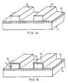
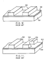
- Figure 10 is a schematic perspective view illustrating a part of a conventional semiconductor device.
- a silicon oxide film 102 is formed on the surface of a silicon substrate 101.
- a metal lead film made of an Al-Si-Cu alloy is formed on the silicon oxide film 102.
- the metal lead film is selectively etched using a photoresist (not shown) as a mask so as to form metal leads 103.
- Figure 10 shows a state in which the photoresist has been eliminated.
- the substrate 101 of Figure 10 is washed with high-purity water. In this process, a corroded portion 104 appears at a portion of the metal leads 103 as shown in Figure 11. This corrosion is caused by F and Cl adhered to the surfaces of metal leads 103.
- metal leads of an Al-Si-Cu alloy As compared to those of an Al-Si alloy and to those of Al (least).
- the reason to use such an alloy is that the electromigration in the metal leads can be significantly suppressed when they are made of an alloy, in particular, of an Al-Si-Cu alloy. Namely, the highest reliability of metal leads can be obtained when an Al-Si-Cu alloy is used.
- metal leads of an alloy have other disadvantages as follows. Specifically, oxidation and reduction can occur in a water solution because of the electrode potential difference between two different metals (i.e., cell effect). For example, in the case of an Al-Si-Cu alloy, corrosion accompanied with the growth of Al(OH)3 occurs when the surfaces of metal leads are exposed to the water solution. This corrosion occurs even when F or Cl does not exist on the metal lead surfaces.
- a technique in which metal is selectively deposited on metal portions or semiconductors has many advantages.
- W is selectively deposited on W or Si by using WF6 gas.
- This technique has advantage as follows. Specifically, the difference in reactive characteristics between a base material and W or Si on which W is deposited can be effectively utilized.
- this technique also has disadvantages as follows. Specifically, this requires a vacuum apparatus. Further, it is difficult to safely handle WF6 gas. Moreover, this technique is only applicable to W, i.e., no other materials can be used.
- metal is selectivley deposited on prescribed portions of a substrate by using laser beams or electron beams. Specifically, metal is deposited only on prescribed portions to which laser beams or electron beams are applied. This technique is applicable to various metals other than W. The experimental results using this technique can be easily obtained.
- one object of this invention is to provide a method of manufacturing semiconductor devices, in particular, a method of processing the surfaces of metal leads, so as to suppress corrosion thereof.
- Another object of this invention is to provide a method of manufacturing semiconductor devices, specifically, a method of selectively depositing various metals other than W on the metal and semiconductor portions of the device.
- a method which comprises the steps of selectively forming metal leads on the surface of a semiconductor substrate, and immersing the semiconductor substrate in a solution containing metal, whereby depositing the metal separated from the solution on the surfaces of the metal leads.
- a semiconductor substrate on which metal films have been formed is immersed in a solution containing metal.
- the metal in the solution is separated therefrom and deposited on the metal films.
- the metal on the metal films on the substrate is substituted by the metal separated from the solution.
- corrosion of the metal film surface can be prevented.
- an Al-Si-Cu alloy film on which halogen elements such as F or Cl are adhered is immersed in a solution containing metal having an ionization tendency equal to or smaller than that of Al. As a result, corrosion of the alloy film can be prevented.
- An alloy of the Al-Si-Cu group has a reliability higher than that of Al or an Al-Si alloy in terms of anti-electromigration.
- an Al-Si-Cu alloy is best used as a material of metal leads in a semiconductor device.
- oxidation and reduction can occur in the solution.
- an Al-Si-Cu alloy has an electro-chemical electrode potential difference between two differeent metals (cell effect).
- corrosion accompanied with the growth of Al(OH3) occurs.
- the metal contained in a solution is appropriately selected with respect to the metal of Al-Si-Cu alloy films, satisfactory results can be obtained as follows. Specifically, the metal can be separated from the solution, and deposited on the surface of an Al-Si-Cu alloy. Further, F or Cl, which is adhered to the surface of this alloy, can be eliminated. In the case of Al or an Al-Si alloy, this metal has less cell effect, and is inherently corrosion-resistant. However, if F or Cl is adhered to the surface of such metal, and when the metal is immersed in a solution, corrosion also occurs.
- the Fe When Al or an Al-Si alloy with F or Cl adhered is immersed in a solution containing Fe, the Fe is also separated from the solution, and deposited on the surface of the metal. In this case, the amount of Fe deposited on the surface of the Al or an Al-Si alloy is smaller than that in the case of an Al-Si-Cu alloy. At the same time, F or Cl adhered to the surface of the Al or an Al-Si alloy is eliminated, and corrosion thereof can be prevented. As described above, if once metal, which has been appropriately selected, is deposited on the surface of an Al-Si-Cu alloy film, the alloy film can be prevented from corrosion even when it is immersed in high-purity water.
- a solution containing metal includes water, an acid water solution or an alkaloid water solution, in each of which salt of metal is dissolved.
- the salt of metal includes nitrate, sulfate and organic acid salt.
- haloid salt is not suitable for such a solution. This is because if the concentration of halogen negative ion in the solution is high, corrosion can no longer be prevented. Further, oxides and hydrate other than the above-described salt of metal may also be used for such a solution.
- the metal contained in a solution exists as ion.
- the metal in the solution must have an ionization tendency smaller than that of metal or a semiconductor on the surface of a substrate to be processed. This is required in order that the metal can be separated from the solution and deposited on the substrate surface in a prescribed manner. This is obvious from the phenomena of electro-chemical oxidation and reduction.
- metals to be deposited on an Al-alloy are metals having an ionization tendency smaller than that of the Al-alloy.
- Such metals are Zn, Fe, Ni, Sn, Pb, Cu, Ag, Pt, Au, W, Mo, Ti, Ho, Cr, Mn and Cd.
- nitrate, organic acid salt or sulfate, each combining one of the above-described metals is dissolved in a water solution. Thereafter, the substrate on which Al-alloy films have been formed is immersed in the thus prepared water solution. As a result, one of the above-described metals is separated from the solution and deposited on the Al-alloy films in a prescribed manner.
- the metal in the solution is separated therefrom and deposited on the surfaces of the metal leads. Further, when a substance other than metal, such an SiO2 film, coexists on the substrate surface, a small amount of the metal in the solution is deposited also on the SiO2 film. Assume that metal leads of an Al-Si-Cu alloy are formed on an SiO2 film provided on a silicon substrate. Further, this substrate is immersed in a solution containing Fe. In this case, Fe in the solution is deposited on the Al-Si-Cu alloy, and at the same time, a small amount (about 1/10 or less) of Fe is deposited also on the SiO2 film.
- the Fe of a specified amount or more on the SiO2 film becomes a contaminant that has some adverse effect on the device configuration.
- the unnecessary Fe deposited on the SiO2 film must be eliminated.
- the amount of such Fe is reduced to about 1/2. In some cases, further reduction of the Fe is required for more accurate circuit configuration. In such cases, the substrate is immersed in a dilute acid solution, which dissolves the Fe.
- this embodiment can also be used as a method of selectively depositing metal on the metal and semiconductor portions on a substrate. Specifically, a large amount of metal is deposited on the metal and semiconductor portions, while a small amount of metal is deposited on tbe insulators, sucb as SiO2 and photoresist films on the substrate. Further, in this embodiment, when appropriate metal is deposited on the surfaces of metal leads made of an Al-Si-Cu alloy, electromigration in the metal leads can be suppressed. Particularly when one of metals such as Ni, Sn or Ho is deposited on the surface of the metal leads of Al-Si-Cu alloy, the metal leads exhibit significant anti-electromigration characteristics. In this case, if the substrate is thermally processed, such electromigration can be more effectively suppressed. This is because the metal deposited on the surfaces of metal leads is thermally diffused into the metal which originally exists in the metal leads.
- a semiconductor substrate on which metal films have been formed is immersed in a solution.
- the solution contains negative ion precluding halogen, i.e., NO3 ⁇ , SO42 ⁇ or COOH ⁇ .
- a passivity layer is formed on the surface of the metal film.
- a passivity is a state in which metal exhibits precious metal properties. In other words, it is a state in which metal is completely covered with a thin transparent film of hydrated oxide.
- corrosion of the metal leads of an Al-Si-Cu alloy on the substrate can be prevented as follows.
- an Al-Si-Cu alloy has high reliability in anti-electromigration, but is liable to corrosion.
- a substrate on which metal leads of an Al-Si-Cu alloy have been formed is immersed in a solution containing NO3 ion.
- NO3 ion As a result, a passivity film is formed on the surfaces of the metal leads.
- corrosion of the metal leads can be prevented.
- the concentration of the NO3 ion in the solution must be 1 ppm. at a minimum. When the concentration of the NO3 ion is insufficient, corrosion of the metal leads can easily occur.
- Such a solution may also contain metal ion accompanied with the NO3 ion. Further, when the metal ion has an ionization tendency smaller than that of the metal on the substrate, corrosion of the metal leads can be significantly prevented.
- Fe is a metal having an ionization tendency smaller than that of Al.
- the solution containing NO3 ion is a water solution in which nitrate of metal is dissolved.
- the water solution may also contain other negative ions besides NO3 ion.
- halogen ion of a high concentration (about 10 ppm. or more) must be avoided in this solution. Otherwise, the metal leads can be corroded.
- a semiconductor substrate which partially exposes metal and semiconductor portions, is processed as follows. First, the substrate is immersed in a solution containing metal. The metal in the solution is chemically reduced at the surfaces of the metal and semiconductor portions, and deposited thereon. In another case, the metal in the solution is substituted by the metal atoms or semiconductor atoms of the respective surfaces, and deposited thereon. In this case, the amount of metal deposited on the insulators on the substrate is far smaller (less than 1/10) than that deposited on the metal and semiconductor portions. Therefore, even when metal and semiconductor portions coexist with insulators on the substrate, the metal in the solution can be selectively deposited on the metal and semiconductor portions on the substrate.
- the following metals are generally used for metal leads and electrodes on the substrate.
- the metals are Al, an Al-alloy, refractory metals (such as W and Mo), and silicides of these metals, or Cu and an Cu alloy.
- These metals are used for various applications as follows. For example, one of these metals is used as a barrier which improves contact characteristics (to lower contact resistance and to enhance adhesion) between the base metal and the metal leads.
- Another metal is used for coating the metal leads so as to suppress their electromigration and stressmigration.
- Another metal is used for controlling the light reflection factor in the process of photoetching. In this embodiment, all these metals can be selectively deposited on the respective metal and semiconductor portions.
- the metal in the solution is deposited also on the insulators
- the amount of tbe metal deposited on the insulators is far smaller than that deposited on the metal and semiconductor portions on the substrate. This occurs, for example. when Fe is deposited on an Al-alloy film, at the same time Fe is deposited also on SiO2 films.
- the amount of Fe deposited on the SiO2 film is far smaller than that deposited on the Al-alloy film.
- the Fe deposited on the SiO2 films can have some adverse effect on the circuit configuration in the later processes.
- the unnecessary metal deposited on the SiO2 film can be eliminated as follows. For example, when the surface of the SiO2 film is washed with high-purity water alone, the metal deposited on the SiO2 film can be reduced to about half.
- the substrate is immersed in a dilute acid solution, which dissolves the unnecessary metal.
- the metal deposited on the SiO2 can be completely eliminated, leaving the necessary metal on the metal and semiconductor on the substrate.
- This selective elimination of the metals can be achieved because of a large difference berween the amounts of the necessary and unnecessary metals.
- Other techniques of eliminating unnecessary metal can be obtained as follows. Specifically, they are a technique of applying charged particles such as electron or ion, a technique of applying a light beam, and a technique of thermal processing. Further, a technique of applying plasma or light in an atmosphere of reactive gas can also be obtained.
- a method of selectively depositing metal on the metal and semiconductor portions on a substrate is provided.
- this embodiment can also be applied to a method of depositing metal on the entire surface of the metal and semiconductor portions on a substrate.
- metal in a solution is deposited on the entire surface of the metal and semiconductor portions on the substrate. Thereafter, the thus metal-deposited surface is patterned by etching or the like.
- a second metal can be deposited selectively or in an isotropic manner by the use of another technique. For example, Ti is deposited on an Al-alloy by use of the method of this invention.
- W is selectively deposited on the thus Ti-deposited Al-alloy by using a reducing reaction of WF6 gas.
- various materials can be used for fabricating a multi-layer configuration by performing depositions several times in accordance with the methods of this invention.
- metal deposited on a layer is caused to be alloyed with the base layer of a substrate. Further, a portion of the metal deposited on the layer is caused to be diffused into the base layer. As a result, a satisfactory adhesion property of the deposited metal layer with respect to the base layer can be achieved.
- These processes are performed by heating the substrate at prescribed temperatures. Specifically, the substrate is heated at temperatures below 500°C to enhance the adhesion property of the deposited layer. The substrate is heated at temperatures higher than 400°C ro achieve the alloying and diffusion into an Al-alloy.
- FIGURE 1a shows a substrate to be processed in accordance with a method of this embodiment.
- an SiO2 film 12 is formed on the surface of a silicon substrate 11.
- Two parallel-arranged metal leads 13 of an Al-Si-Cu alloy are formed on the SiO2 film 12.
- the metal leads 13 are formed as follows. Specifically, an Al-Si-Cu alloy film is formed on the entire surface of the SiO2 film 12. Thereafter, photoresist is painted on the entire surface of the alloy film. The thus painted photoresist is etched by a conventional photoetching process to form prescribed patterns. Next, the Al-Si-Cu alloy film is selectively etched using a patterned photoresist as a mask.
- the substrate 11 of FIGURE 1a is washed with a water solution in which Fe is dissolved as nitrate. (Fe : 5 ppm; NO3 : 30 ppm).
- Fe Fe
- the Fe in the water solution is separated therefrom, and is deposited on the surfaces of the metal leads 13.
- thin Fe films 15 are formed on the surfaces of the metal leads 13, as shown in FIGURE 1b.
- the thin Fe films 15 are not corroded even when they are washed with high-purity water.
- the metal leads 13 are not corroded.
- a large amount of Fe is deposited on the metal leads 13 of Al-Si-Cu alloy while a far smaller amount of Fe is deposited on the SiO2 film 12.
- the Fe deposited on the SiO2 film 12 can be reduced to about half only by washing the substrate 11 with high-purity water. Further, when the substrate 11 is immersed in a very dilute acid solution (e.g., HF), Fe deposited on the SiO2 film 12 can be eliminated completely. At the same time, the Fe deposited on the metal leads 13 of Al-Si-Cu alloy is also reduced. However, the amount of Fe deposited on the metal leads 13 is sufficiently larger than that of the SiO2 film 12. Thus, this causes no problems.
- a very dilute acid solution e.g., HF
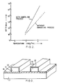
- the metal leads 13 of Al-Si-Cu alloy on which Fe is deposited exhibit significantly greater anti-electromigration characteristics than those without Fe deposition. Further, the substrate 11 metal leads 13 of Al-Si-Cu alloy on which Fe has been deposited is exposed to an atmosphere of N2 at 450°C for about 30 minutes. As a result, the metal leads 13 with Fe can be anneaied, and the anti-electromigration characteristics thereof can be more enhanced as shown in a graph of FIGURE 2.
- the ordinate represents MTTF (mean time to failure) in hours, which corresponds to an average time elapsed to break the metal leads, and the abscissa represents temperature.
- the solid line represents the case in which the metal leads are annealed, and the dotted line represents the case in which the metal leads are not annealed.
- a solution containing Fe has been used.
- a solution containing various metals other than Fe can also be used.
- Such various metals must have an ionization tendency smaller than or equal to Al.
- salt of an appropriate metal selected from such various metals is dissolved in a water solution.
- a prescribed solution containing metal ion can be prepared.
- nitrate, sulfate or organic acid salt is used as salt.
- haloid salt is not suitable for such a solution. This is because if the concentration of halogen negative ion in a solution is high, this solution can cause corrosion of the metal leads on the substrate.
- Even in the case of Fe if salt chloride is used to prepare a solution having a concentration of about 5 ppm, this solution can also cause corrosion of the metal leads.
- metals other than Fe can be used to prepare a solution containing metal ion.
- metals are Al, Zn, Ni, Sn, Pb, Cu, W, Ag, Pt, Au, Cd, Cr, Ho, Mn, Mo, Ti,Nb, Sr and Ta.
- the solution must have a concentration of several ppm. at most to avoid occurrence of corrosion of the metal leads.
- the pH of such a solution must be predetermined to be dilute acid or alkaline before the specified salt is dissolved in the solution. In such cases, even when the pH of the solution is dilute acid or alkaline, tbe prescribed metal deposition and the prevention of corrosion can be achieved.
- a substrate is washed with high-purity water.
- the amount of metal deposited on the SiO2 film on the substrate can be reduced to about half.
- the substrate is immersed in a dilute acid solution which dissolves the metal.
- the metal deposited on the SiO2 film on the substrate is completely eliminated.
- the metal deposited on the SiO2 film can also be eliminated by dry-washing techniques, such as a plasma-applying technique or a light beam-applying technique.
- the substrate of FIGURE 1a is immersed in a solution which dissolves nitrate of Al (Al : 1 ppm., NO3 : 30 ppm.) As a result, passivity films 25 are formed on metal leads 13 of Al-Si-Cu alloy. The existence of passivity films 25 can prevent corrosion of the metal leads 13. Thus even when the substrate is washed with high-purity water, the widths of metal lead 13 are not reduced.
- the Al in the solution is separated therefrom, and selectively deposited on the metal leads 13 of Al-Si-Cu alloy and the SiO2 film 12. The amount of Al deposited on the SiO2 film 12 is far smaller than that of the metal leads 13.
- the amount of Al deposited on the SiO2 film 12 can be reduced to about half only by washing the substrate 11 with high-purity water. Further, if the substrate 11 is immersed in a very dilute acid solution (e.g., HF), the Al deposited on the SiO2 film 12 can be eliminated completely. At the same time, Al deposited on the metal leads 13 of Al-Si-Cu alloy is also reduced. However, the amount of Al deposited on the metal leads 13 is sufficiently larger than that of the SiO2 film 12. Thus, this reduction of Al causes no problems.
- a very dilute acid solution e.g., HF
- the metal leads of Al-Si-Cu alloy exhibit anti-electromigration characteristics greater than that in the case of without Al-deposition.
- Metal leads with and without Al-deposition were examined as to their reliability. As a result, it has been confirmed that the metal leads with Al-deposition can withstand for a time about twice longer than those without Al-deposition.
- the thus formed passivity films become disadvantages when making contact with other metals in the later process.
- the passivity films can be easily eliminated by using techniques as follows. Specifically, typical eliminating techniques are an etching by use of a solution, a physical technique such as Ar-sputtering, an electric discharge-chemical technique, and an RIE technique. Further, they include a light beam-applying technique, and an electron beam-applying technique.
- FIGURES 4a through 4c are cross-sectional views illustrating the processes of forming a metal lead.
- a first SiO2 film 42 is formed on an Si substrate 41 as shown in FIGURE 4a.
- An opening is made in a portion of th first SiO2 film 42.
- a metal layer 43 and a second metal layer 44 are sequentially formed by a sputtering technique.
- the first and second layers 43 and 44 are patterned.
- the first metal layer 43 is made of Ti or a Ti-alloy
- the second metal layer 44 is made of an Al-alloy (e.g., Al-Si-Cu alloy).
- a third metal layer 45 of Ti is formed wrapping the second metal layer 44 by use of a method according to the present invention.
- the substrate 41 is immersed in a solution containing nitrate of Ti.
- the Ti is separated from the solution, and is deposited wrapping the second metal layer 44 so as to form the third metal layer 45.
- most of the Ti in the solution is deposited only on the surface of the second metal layer 44, but not on the SiO2 film 42.
- the third metal layer 45 is selectively formed on the surface of second metal layer 44. In other words, only the surface of second metal layer 44 can be convered with the third metal layer 45.
- the concentration of this Ti solution is about 10 ppm.
- the thickness of the third metal layer 45 of Ti is about 500 ⁇ .
- a second SiO2 film 46 is formed on the entire surfaces of the first SiO2 film 42 the third metal layer 45, as shown in FIGURE 4b. This is performed by use of a plasma CVD (chemical vapor deposition) technique.
- a third SiO2 film 47 is formed so as to even the surface of second SiO2 film 46. This surface-evening process is performed by using a spin-on glass.
- the second and third SiO2 films 46 and 47 are selectiveiy etched so as to make an opening therein. As a result, a part of the third metal layer 45 is exposed to the thus made opening.
- a fourth metal layer 48 is selectively formed as follows. Specifically, the substrate 41 is immersed in a solution containing sulfate of W. The W in the solution is separated therefrom, and deposited on the exposed portion of the third metal layer 45. As a result, a fourth metal layer 48 of W is formed.
- a fifth metal layer 49 of W is filled in the opening as shown in FIGURE 4c.
- This process of filling up the opening is performed by use of a selective deposition technique using WF6 gas.
- sixth and seventh metal layers 50 and 51 are sequentially adhered to the fifth metal layer 49 by using a sputtering technique.
- the sixth and seventh metal layers 50 and 51 are patterned in a prescribed manner.
- the first metal layer 43 serves as a barrier metal that reduces the contact resistance between the Si substrate 41 and the second metal layer 44.
- the second metal layer 44 serves as a metal lead in a first layer configuration.
- the third metal layer 45 serves as a metal that enhances both anti-electromigration and anti-stressmigration characteristics of the second metal layer 44.
- the fourth metal layer 48 serves as a barrier metal that reduces the contact resistance between the third metal layer 45 and the fifth metal layer 49.
- the fifth metal layer 49 serves as via-contact metal that bridges a gap between the first metal lead (the metal layer 44) and second metal lead (the metal layer 51) interposing metal layer 45, 48 and 50.
- the sixth metal layer 50 serves as a barrier metal that reduces the contact resistance between the fifth metal layer 49 and the seventh metal layer 51 (the second metal lead).
- the second SiO2 film 46 is an insulating film that exhibits satisfactory insulation characteristics.
- the third SiO2 film 47 is an insulating film that levels the uneven portions of the device.
- the third metal layer 45 of Ti can be selectively deposited on tbe surface of the second metal layer 44 of Al.
- the second metal layer 44 which serves as the metal lead of the first layer, exhibits significantly both the anti-electromigration and anti-stressmigration characteristics.
- the fourth metal layer 48 of FIGURE 4b can be selectively formed on the exposed surface of the third metal layer 45. This process can be easily performed by use of the method of this invention, which is significantly simpler than the conventional techniques.
- the fourth metal layer 48 serves to achieve a satisfactory contact between the second matal layer 44 of Ti and the fifth metal layer 49 of W (FIGURE 4c).
- the metal in the solution is deposited also on the surface of an SiO2 film.
- the metal deposired on te surface of the SiO2 film which is far less than that on the metal layer, can be easily eliminated as follows. Specifically, the surface of the SiO2 film is washed with high-purity water. Further, a substrate on which the SiO2 film have been formed is immersed in a dilute HF solution. As a result, the metal deposited on the SiO2 film can be eliminated completely. However, most of the metal deposited on the metal layer remains. The adhesion property between this metal and the metal layer can be improved when the substrate is thermally processed at about 500°C.
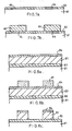
- FIGURES 5a and 5b illustrate a method of selectively depositing a metal layer.
- an SiO2 film 62 is formed on an Si substrate 61, and an opening is made in the SiO2 film 62.
- metal is selectively deposited filling up the opening of the SiO2 film 62 so as to form a metal layer 63 as follows.
- the Si substrate 61 of FIGURE 1a is immersed in a solution containing Al.
- the Al in the solution is separated therefrom, and deposited filling up the opening of the SiO2 film 62.
- the metal layer 63 is formed as shown in FIGURE 5b.
- the solution contains Al+ of 10 ppm and NO3 of 60 ppm.
- an Al layer is formed on an Si substrate.
- the base layer is metal, an Al-layer can be selectively deposited in the same manner as above. It has also been confirmed that various metals other than Al can be similarly deposited.
- FIGURE 6a an SiO2 film 62 is formed on an Si substrate 61, and an opening is made in the SiO2 film 62.
- first metal 64 is deposited in the opening at the bottom thereof, as shown in FIGURE 6b.
- second metal 65 is deposited filling up the opening, as shown in FIGURE 6c.
- first metal is deposited filling up the openings of an SiO2 film 62 so as to form first metal layers 64.
- second metal is deposited on the SiO2 film 62.
- metal is deposited on the surfaces of metal layers made of an Al-Si-Cu alloy.
- an SiO2 film 82 is formed on an Si substrate 81, and an Al-Si-Cu alloy layer 83 is formed on the SiO2 film 82.
- metal is deposited on the entire surface of the Al-Si-Cu alloy layer 83 so as to form a metal layer 84.
- various metals such as Zn, Fe, Ni, Ti, W, Ho and Mo can be deposited. The method of depositing these metals can be performed in the same manner as those described in the previous embodiments.
- the thickness of metal layers deposited is in the range of about 10 to about 1000 ⁇ .
- a photoresist is painted uniformly on the entire surface of the metal layer 84 so as to form a photoresist film 85.
- the photoresist film 85 is patterned in a prescribed manner as shown in FIGURE 8b.
- the metal layer 84 is selectively etched to form metal leads using the patterned photoresist film 85 as a mask. This is performed by use of an RIE technique.
- the photoresist 86 is eliminated by use of an ashing apparatus or the like, as shown in FIGURE 8c.
- metal films such as passivity films are formed on metal leads or metal layers provided on a substrate. This is performed by immersing the substrate in a solution.
- ultrasonic waves are applied to the substrate which is being immersed in a solution.
- metal in a solution is deposited not only on metal portion but also on other portions such as SiO2 films.
- the unnecessary metal deposited on the SiO2 film can be eliminated by use of various techniques.
- ultrasonic waves are applied to a substrate which is being immersed in a solution. As a result, the amount of unnecessary metal deposited on portions other than the prescribed portions can be significantly reduced.
- ultrasonic waves can be easily applied to the substrate by using a conventional ultrasonic washing machine.
- the ultrasonic waves must have minimum frequencies of 600kHz.
- the ultrasonic waves of less than 600kHz can probably destroy metal leads on the substrate in the manufacturing processes.
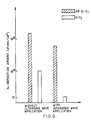
- FIGURE 9 shows experimental results in which the amounts of metal deposited on a metal layer and an SiO2 film were measured in the cases of with and without ultrasonic wave application.
- the substrate of FIGURE 1a was immersed in a solution containing nitrate of Fe (Fe : 5 ppm., NO3 : 30 ppm.). Thereafter, ultrasonic waves were applied to the metal leads of an Al-Si-Cu alloy and the SiO2 film on the substrate.
- the amount of Fe deposited on the SiO2 film was about 1/10 times that on the metal leads of an Al-Si-Cu alloy.
- the amount of Fe deposited on the SiO2 film was about 1/100 times that on the metal leads.
- the Fe deposited on the SiO2 film can be reduced to about half by washing in with high-purity water.
- further reduction of Fe deposited on the SiO2 film is required for more accurate circuit configuration.
- the substrate is immersed in a dilute HF solution, for example, so as to eliminate the Fe deposited on the SiO2 film.
- the amount of Fe deposited on the SiO2 film can be sufficiently reduced by the application of ultrasonic waves. Therefore, the processes of manufacturing semiconductor devices can be significantly simplified.
Landscapes
- Internal Circuitry In Semiconductor Integrated Circuit Devices (AREA)
- Electroplating Methods And Accessories (AREA)
- Chemically Coating (AREA)
Applications Claiming Priority (4)
| Application Number | Priority Date | Filing Date | Title |
|---|---|---|---|
| JP153512/88 | 1988-06-23 | ||
| JP63153512A JP2771989B2 (ja) | 1988-06-23 | 1988-06-23 | 金属膜の表面処理方法 |
| JP246454/88 | 1988-09-30 | ||
| JP63246454A JPH0294524A (ja) | 1988-09-30 | 1988-09-30 | 半導体装置の製造方法 |
Publications (3)
| Publication Number | Publication Date |
|---|---|
| EP0348119A2 true EP0348119A2 (de) | 1989-12-27 |
| EP0348119A3 EP0348119A3 (de) | 1991-07-17 |
| EP0348119B1 EP0348119B1 (de) | 1997-08-13 |
Family
ID=26482111
Family Applications (1)
| Application Number | Title | Priority Date | Filing Date |
|---|---|---|---|
| EP89306148A Expired - Lifetime EP0348119B1 (de) | 1988-06-23 | 1989-06-16 | Verfahren zur Herstellung von metallischen Verbindungen auf Halbleiterbauelemente |
Country Status (3)
| Country | Link |
|---|---|
| EP (1) | EP0348119B1 (de) |
| KR (1) | KR920005351B1 (de) |
| DE (1) | DE68928253T2 (de) |
Families Citing this family (1)
| Publication number | Priority date | Publication date | Assignee | Title |
|---|---|---|---|---|
| KR100425977B1 (ko) * | 2002-02-21 | 2004-04-06 | 김남원 | 고 점도 항문 세정제 조성물 및 세정방법 |
Family Cites Families (6)
| Publication number | Priority date | Publication date | Assignee | Title |
|---|---|---|---|---|
| NL243410A (de) * | 1959-09-16 | 1900-01-01 | ||
| US3400012A (en) * | 1964-06-10 | 1968-09-03 | Minnesota Mining & Mfg | Process of plating metal objects |
| US3632436A (en) * | 1969-07-11 | 1972-01-04 | Rca Corp | Contact system for semiconductor devices |
| DE3202484A1 (de) * | 1982-01-27 | 1983-08-04 | Bayer Ag, 5090 Leverkusen | Metallisierte halbleiter und verfahren zu ihrer herstellung |
| ATE46791T1 (de) * | 1985-07-29 | 1989-10-15 | Siemens Ag | Verfahren zum selektiven auffuellen von in isolationsschichten geaetzten kontaktloechern mit metallisch leitenden materialien bei der herstellung von hoechstintegrierten halbleiterschaltungen sowie eine vorrichtung zur durchfuehrung des verfahrens. |
| US4692349A (en) * | 1986-03-03 | 1987-09-08 | American Telephone And Telegraph Company, At&T Bell Laboratories | Selective electroless plating of vias in VLSI devices |
-
1989
- 1989-06-16 DE DE68928253T patent/DE68928253T2/de not_active Expired - Fee Related
- 1989-06-16 EP EP89306148A patent/EP0348119B1/de not_active Expired - Lifetime
- 1989-06-23 KR KR1019890008721A patent/KR920005351B1/ko not_active Expired
Also Published As
| Publication number | Publication date |
|---|---|
| KR910001920A (ko) | 1991-01-31 |
| DE68928253T2 (de) | 1998-01-15 |
| EP0348119A3 (de) | 1991-07-17 |
| DE68928253D1 (de) | 1997-09-18 |
| EP0348119B1 (de) | 1997-08-13 |
| KR920005351B1 (ko) | 1992-07-02 |
Similar Documents
| Publication | Publication Date | Title |
|---|---|---|
| US5681779A (en) | Method of doping metal layers for electromigration resistance | |
| US5766379A (en) | Passivated copper conductive layers for microelectronic applications and methods of manufacturing same | |
| EP0918081B1 (de) | Ätzmittel und ihre Verwendung | |
| EP0535864B1 (de) | Herstellung eines leitenden Gebietes in elektronischen Vorrichtungen | |
| US4433004A (en) | Semiconductor device and a method for manufacturing the same | |
| EP0395560B1 (de) | Zwischenmetallische Mehrschicht-Verbindung für Halbleitervorrichtungen | |
| KR910002455B1 (ko) | 반도체장치 제조방법 | |
| US7205228B2 (en) | Selective metal encapsulation schemes | |
| US5650356A (en) | Method for reducing corrosion in openings on a semiconductor wafer | |
| KR930011054B1 (ko) | 상이한 층 레벨에 위치한 배선층간의 전기 접촉을 형성하는 방법 | |
| JPH0581664B2 (de) | ||
| US3918149A (en) | Al/Si metallization process | |
| JPH08512435A (ja) | 高周波反応性スパッタリングされたタリウム、タングステンおよび金を備えたマイクロ回路用配線のための耐エレクトロマイグレーション金属被覆構造体 | |
| US5290733A (en) | Method of manufacturing semiconductor devices including depositing aluminum on aluminum leads | |
| EP0499249A2 (de) | Verfahren zum Herstellen einer Halbleitervorrichtung mit einer Sperrschicht | |
| US5430258A (en) | Copper interconnection structure and method of preparing same | |
| US5863834A (en) | Semiconductor device and method of manufacturing the same | |
| US4121241A (en) | Multilayer interconnected structure for semiconductor integrated circuit | |
| JPH06181212A (ja) | 半導体装置の製造方法 | |
| EP0425162A2 (de) | Verbesserte Aluminiummetallisierung für Halbleitervorrichtungen | |
| EP0348119A2 (de) | Verfahren zur Herstellung von metallischen Verbindungen auf Halbleiterbauelemente | |
| JPH11312734A (ja) | 半導体ウエハの絶縁層バイア内の銅層への接点を形成する方法及び構造 | |
| JP2534434B2 (ja) | 耐酸化性化合物およびその製造方法 | |
| EP0249256B1 (de) | Halbleiteranordnung mit einer Aluminium-Verbindungsschicht mit geringem Vanadium-Prozentgehalt | |
| JP2771989B2 (ja) | 金属膜の表面処理方法 |
Legal Events
| Date | Code | Title | Description |
|---|---|---|---|
| PUAI | Public reference made under article 153(3) epc to a published international application that has entered the european phase |
Free format text: ORIGINAL CODE: 0009012 |
|
| 17P | Request for examination filed |
Effective date: 19890626 |
|
| AK | Designated contracting states |
Kind code of ref document: A2 Designated state(s): DE FR |
|
| PUAL | Search report despatched |
Free format text: ORIGINAL CODE: 0009013 |
|
| AK | Designated contracting states |
Kind code of ref document: A3 Designated state(s): DE FR |
|
| 17Q | First examination report despatched |
Effective date: 19940210 |
|
| GRAG | Despatch of communication of intention to grant |
Free format text: ORIGINAL CODE: EPIDOS AGRA |
|
| GRAH | Despatch of communication of intention to grant a patent |
Free format text: ORIGINAL CODE: EPIDOS IGRA |
|
| GRAH | Despatch of communication of intention to grant a patent |
Free format text: ORIGINAL CODE: EPIDOS IGRA |
|
| GRAA | (expected) grant |
Free format text: ORIGINAL CODE: 0009210 |
|
| AK | Designated contracting states |
Kind code of ref document: B1 Designated state(s): DE FR |
|
| REF | Corresponds to: |
Ref document number: 68928253 Country of ref document: DE Date of ref document: 19970918 |
|
| ET | Fr: translation filed | ||
| PLBE | No opposition filed within time limit |
Free format text: ORIGINAL CODE: 0009261 |
|
| STAA | Information on the status of an ep patent application or granted ep patent |
Free format text: STATUS: NO OPPOSITION FILED WITHIN TIME LIMIT |
|
| 26N | No opposition filed | ||
| REG | Reference to a national code |
Ref country code: FR Ref legal event code: D6 |
|
| PGFP | Annual fee paid to national office [announced via postgrant information from national office to epo] |
Ref country code: FR Payment date: 20020610 Year of fee payment: 14 |
|
| PG25 | Lapsed in a contracting state [announced via postgrant information from national office to epo] |
Ref country code: FR Free format text: LAPSE BECAUSE OF NON-PAYMENT OF DUE FEES Effective date: 20040227 |
|
| REG | Reference to a national code |
Ref country code: FR Ref legal event code: ST |
|
| PGFP | Annual fee paid to national office [announced via postgrant information from national office to epo] |
Ref country code: DE Payment date: 20060608 Year of fee payment: 18 |
|
| PG25 | Lapsed in a contracting state [announced via postgrant information from national office to epo] |
Ref country code: DE Free format text: LAPSE BECAUSE OF NON-PAYMENT OF DUE FEES Effective date: 20080101 |