EP0347935B1 - Semiconductor memory device - Google Patents
Semiconductor memory device Download PDFInfo
- Publication number
- EP0347935B1 EP0347935B1 EP89111475A EP89111475A EP0347935B1 EP 0347935 B1 EP0347935 B1 EP 0347935B1 EP 89111475 A EP89111475 A EP 89111475A EP 89111475 A EP89111475 A EP 89111475A EP 0347935 B1 EP0347935 B1 EP 0347935B1
- Authority
- EP
- European Patent Office
- Prior art keywords
- dummy
- cells
- potential
- column line
- column
- Prior art date
- Legal status (The legal status is an assumption and is not a legal conclusion. Google has not performed a legal analysis and makes no representation as to the accuracy of the status listed.)
- Expired - Lifetime
Links
- 239000004065 semiconductor Substances 0.000 title claims description 33
- 230000008859 change Effects 0.000 claims description 2
- 239000000872 buffer Substances 0.000 description 14
- 238000005513 bias potential Methods 0.000 description 9
- 230000001052 transient effect Effects 0.000 description 7
- 230000007257 malfunction Effects 0.000 description 6
- 238000010586 diagram Methods 0.000 description 5
- 230000000694 effects Effects 0.000 description 3
- 230000007423 decrease Effects 0.000 description 2
- 238000007599 discharging Methods 0.000 description 2
- 229910021420 polycrystalline silicon Inorganic materials 0.000 description 2
- 229920005591 polysilicon Polymers 0.000 description 2
- 239000000758 substrate Substances 0.000 description 2
- 230000007704 transition Effects 0.000 description 2
- WQJQOUPTWCFRMM-UHFFFAOYSA-N tungsten disilicide Chemical compound [Si]#[W]#[Si] WQJQOUPTWCFRMM-UHFFFAOYSA-N 0.000 description 2
- 229910021342 tungsten silicide Inorganic materials 0.000 description 2
- 239000003990 capacitor Substances 0.000 description 1
- 230000001419 dependent effect Effects 0.000 description 1
- 230000006870 function Effects 0.000 description 1
- 230000006872 improvement Effects 0.000 description 1
- 239000012535 impurity Substances 0.000 description 1
- 238000004519 manufacturing process Methods 0.000 description 1
- 239000000463 material Substances 0.000 description 1
- 239000011159 matrix material Substances 0.000 description 1
- 230000004048 modification Effects 0.000 description 1
- 238000012986 modification Methods 0.000 description 1
- 230000000630 rising effect Effects 0.000 description 1
Images


Classifications
-
- G—PHYSICS
- G11—INFORMATION STORAGE
- G11C—STATIC STORES
- G11C7/00—Arrangements for writing information into, or reading information out from, a digital store
-
- G—PHYSICS
- G11—INFORMATION STORAGE
- G11C—STATIC STORES
- G11C7/00—Arrangements for writing information into, or reading information out from, a digital store
- G11C7/12—Bit line control circuits, e.g. drivers, boosters, pull-up circuits, pull-down circuits, precharging circuits, equalising circuits, for bit lines
-
- G—PHYSICS
- G11—INFORMATION STORAGE
- G11C—STATIC STORES
- G11C16/00—Erasable programmable read-only memories
- G11C16/02—Erasable programmable read-only memories electrically programmable
- G11C16/06—Auxiliary circuits, e.g. for writing into memory
- G11C16/26—Sensing or reading circuits; Data output circuits
- G11C16/28—Sensing or reading circuits; Data output circuits using differential sensing or reference cells, e.g. dummy cells
-
- G—PHYSICS
- G11—INFORMATION STORAGE
- G11C—STATIC STORES
- G11C7/00—Arrangements for writing information into, or reading information out from, a digital store
- G11C7/06—Sense amplifiers; Associated circuits, e.g. timing or triggering circuits
- G11C7/062—Differential amplifiers of non-latching type, e.g. comparators, long-tailed pairs
-
- G—PHYSICS
- G11—INFORMATION STORAGE
- G11C—STATIC STORES
- G11C7/00—Arrangements for writing information into, or reading information out from, a digital store
- G11C7/14—Dummy cell management; Sense reference voltage generators
Definitions
- the present invention relates to a semiconductor memory device improved in a reference potential generating circuit for a sense amplifier and load circuits for memory cells.
- a semiconductor memory device which comprises memory cells, column lines receiving data from said memory cells and a load circuit coupled with said column lines. Furthermore, dummy cells are provided which are connected to a dummy column line. A further load circuit and a further dummy cell are also connected to the dummy column line. The gate of the additional dummy cell is supplied with a present potential. Furthermore, a sense amplifier is provided for sensing the data stored in said memory cell in accordance with the potential difference between the column line and the dummy column line.
- Such a conventional semiconductor memory device shown in Fig. 1 is an erasable and programmable ROM (EPROM) using floating gate MOSFETs as memory cells.
- EPROM erasable and programmable ROM
- MC11, MC12, ..., MC1n designate floating gate MOSFETs; DC a floating gate MOSFET as a dummy cell; WL1, WL2, ..., WLm row lines; BL1, BL2, ..., BLn column lines; DBL a dummy column line; 11 a row decoder; 12 a column decoder; BT1, BT2, ..., BTn column gate MOSFETs for column selection; DBT a MOSFET that is equivalent to the column gate MOSFET and is normally in a conductive state with application of a power voltage Vcc to the gate of the MOSFET; 13A a first bias setting circuit made up of n-channel MOSFETs QM1 to QM6; 14A a first load circuit made up of a p-channel MOSFET QM7; 13B a second bias setting circuit made up of n-channel MOSFETs QD1 to QD6; 14B a second load circuit made up of
- MOSFETs whose channels are not specified will be treated as n-channel MOSFETs.
- the dummy cell DC consists of a MOSFET equivalent to that of a memory cell MC that is any of the memory cells MC11 to MCmn.
- the dummy column line DBL is equivalent to the column line BL that is any of those column lines BL1 to BLn.
- the node potential V2 is set a a voltage which is the sum of a potential on the column line BL when a Predetermined current flows into the memory cell MC, and a threshold voltage of the n-channel MOSFET containing an increased threshold voltage due to the substrate bias effect.
- the MOSFET QM4 is an initial charging MOSFET for quickening an initial charging to the column line BL in which the column line BL is charged from an initial voltage 0 V.
- the initial charging MOSFET is rendered nonconductive when the column line potential exceeds a potential on the column line when a predetermined current flows into the memory cell MC.
- a reference potential Vref is generated by the second load circuit 14B on the basis of the data in the dummy cell DC, and appears at a node B.
- An input potential Vin is generated by the first load circuit 14A on the basis of the data read out of a memory cell MC as selected by the output signals of the row decoder 11 and the column decoder 12, and appears at a node A.
- the sense amplifier 15 compares the reference potential Vref and the input potential Vin to sense a type of the data stored in the memory cell MC.
- the sensed data is amplified by the sense amplifier 15, and outputted through the output buffer 16.
- each memory cell of the EPROM data is programmed by selectively injecting electrons into the floating gate of the cell.
- a high voltage e.g., 12.5 to 21 V, which is much higher than the normal power voltage, e.g., 5 V
- the normal power voltage e.g. 5 V
- an impact ionization occurs in the vicinity of the drain of the memory cell located at a cross point of the selected row and column lines, to generate electron-hole pairs. Of the generated electron-hole pairs, the electrons are injected into the floating gate of the memory cell.
- a threshold voltage of the memory cell injected with electrons is much higher than that of the memory cell not injected.
- the memory cell whose floating gate is injected with electrons maintains an off-state even if a signal of "1" level (power voltage Vcc) is supplied to the control gate of the cell, or the row line. Under the same condition, the memory cell not injected with electrons is turned on. Since the dummy cell DC is not injected with electrons, no potential difference is caused between the potentials Vref and Vin.
- a channel width WD7 of the MOSFET QD7 in the second load circuit 14B is set to be larger than that WM7 of the MOSFET QM7 in the first load circuit 14A.
- a conduction resistance of the MOSFET QD7 is smaller than that of the MOSFET QM7.
- the conduction resistance of the MOSFET QD7 is so selected that the reference potential Vref is between the Vin potential when the electron injected memory cell is selected and the Vin potential when the no electron injected memory cell is selected.
- the potential Vin represents a potential which is the result of a subtraction of the threshold voltage of the load MOSFET QM7 from the power source voltage Vcc.
- the electron injected memory cell or the memory cell with a high threshold level will be assumed to be a memory cell storing "0" data.
- the no electron injected memory cell or the memory cell with a low threshold voltage will be assumed to be a memory cell storing "1" data.
- the data read out by the sense amplifier is received by the buffer 16, and the buffer 16 outputs the data.
- the output buffer 16 it is necessary to charge and discharge an external large load capacitor. Therefore, when the output buffer 16 produces the data, noise is generated in the power source. The noise causes a variation in the power source voltage Vcc.
- the conduction resistance of the MOSFET QD7 in the second load circuit 14B is different from that of the MOSFET QM7 in the first load circuit 14A. Therefore, these transistors respond to the power voltage variation in a different way. In an extreme case, a proper amplitude relationship between the potentials Vin and Vref is reversed, so that the sense amplifier may produce erroneous data. Such a malfunction of the sense amplifier should be avoided.
- the EPROM of Fig. 1 will encounter a situation that a row line connected to the memory cells of "1" data that is currently selected is switched to another row line connected to the memory cell having the same data, and subsequently the data are successively read out from the memory cells on the new row.
- the memory cells selected anew are insufficiently turned on in the initial stage, until the potential of the row line selected anew reaches power source voltage Vcc. Consequently, the potential of the selected bit line is temporarily increased.
- the threshold voltage of the memory cell of the floating gate structure is approximately 2 V.
- the reference potential Vref is always constant as shown in Fig. 2 showing waveforms of potentials Vref and Vin.
- the sense amplifier 15 temporarily produces the data of an improper logic level.
- the output data of the buffer 16 varies its logic level, "1" ⁇ "0" ⁇ "1", during a short period. Therefore, an inductance component existing in the lead creates a great variation of the earth voltage, possibly causing a malfunction of a circuit in the EPROM.
- the dummy cells DC1 to DCm are provided corresponding to row lines WL1 to WLm, respectively.
- the control gates of the dummy cells DC1 to DCm are connected to the row lines WL1 to WLm, respectively.
- the drains of the dummy cells DC1 to DCm are connected to a dummy column line DBL.
- the dummy cells are controlled by the signals on the row lines. Even in the situation that the row lines are switched from one to the other, and succeeding to the memory cell storing data "1" on the previous or old row line, the memory cell storing the data "1" on the present or new row line are subjected to the read operation, the dummy column line DBL is charged by the load circuit 14B at the time of switching the row lines. Accordingly, as seen from Fig. 4 showing waveforms, the reference potential Vref rises as the potential Vin ("1" level) rises. In the EPROM, the potential Vin does not cross the curve of the reference potential Vref.
- the output data of the output buffer 16 is invariable, and no variation of the earth voltage is caused.
- the rise of the potentials Vin and Vref is caused by the charging operation at the time of switching of the row lines, and hence the degree of the potential rise is different dependent on the conduction resistances of the MOSFETs QM7 and QD7 in the load circuits 14A and 14B.
- the conduction resistance of the MOSFET QD7 is set much smaller than that of MOSFET QM7.
- the reference potential Vref rises to a level (denoted by Vref in Fig. 5) much higher than a level (denoted by a broken line in Fig. 5) in which the reference potential Vref in the Fig. 1 circuit is. Therefore, the reading speed for "0" data of the circuit shown in Fig. 3 is lower by time T1 (Fig. 5) than that of the circuit shown in Fig. 1.
- a characteristic curve depicted by a solid line in Fig. 6 shows a voltage vs. current characteristic curve of the first load circuit 14A in the conventional semiconductor memory device.
- the abscissa represents a potential Vin at the node A and the ordinates a load current flowing into the load circuit. It is assumed that Vin ("1" level) is a potential at the node A caused when the memory cell of a low threshold voltage is selected and a memory cell current Icell flows, and Vin (“0" level) is a potential at the node A and Vref is a potential at the node B.
- the column line is switched one from the other, and the memory cell of a high threshold voltage is selected, the charging to the new selected column line starts at the voltage of 0 V.
- Capacitance connected to the column lines has become large, with the increase of the semiconductor memory capacity. Accordingly, to realize a high speed read operation, it is necessary to quicken both the charging speed of the column line and the read operation for reading out the "0" data.
- the column line is charged at a high speed through the initial charging transistor QM4 when the potential is less than Vin ("1" level). When the potential of the column line BL exceeds Vin ("1" level), the transistor QM4 becomes nonconductive.
- the p-channel transistor QM7 in the load circuit 14A charges the column line BL. Since the gate of the p-channel transistor QM7 is connected to the drain thereof, when the potential Vin at the node A rises, a conduction resistance of this transistor QM7 rapidly increases, and a charge current rapidly decreases. Therefore, it takes much time for the potential at the node A to rise from Vin ("1" level) to Vin ("0" level), lowering the data read speed. In other words, the time taken for the node A potential to rise from Vin ("1" level) to Vin (“0" level) can be reduced by increasing the channel width of the transistor QM7 and reducing its conduction resistance. However, the decrease of the conduction resistance of the transistor QM7 creates another problem that a margin for the power source noise is narrowed.
- a characteristic curve as indicated by a dotted line is obtained for the transistor QM7 whose conduction resistance is 1/2 that of the same transistor when the cell current vs. input voltage Vin characteristic thereof is indicated by a solid line.
- the 1/2 conduction resistance of the transistor QM7 is set, the potential Vin at the node A when the memory cell storing the "1" data, viz., the memory cell of a low threshold voltage, is selected, is Vin ("1" level)′.
- the potential Vref′ at the node B is set at exactly the middle point between the potential Vin ("1" level)′ at the node A when the memory cell of "1" data is selected and that Vin ("0" level) when the memory cell storing "0" data, i.e., the memory cell of a low threshold voltage. Accordingly, the conduction resistance of the p-channel MOS transistor QD7 in the second load circuit 14B is so selected that the potential at node B when the 1/2 conduction resistance of transistor QM7 is set, is equal to Vref′ as ⁇ Vin ("0" level) - Vin("1" level) ⁇ /2.
- the semiconductor memory device As described above, in the conventional semiconductor memory device improved in the read speed by using a small conduction resistance in the load circuit, the semiconductor memory device is apt to malfunction due to the power noise.
- an object of the present invention is to provide a semiconductor memory device which is free from the power noise even during a transient period that row lines are switched from one to the other, and is operable at an increased data read speed.
- the second dummy cell which is set in an on state normally or during a transient period of switching row lines from one to the other, is connected to the dummy column line.
- the connection of the second dummy cell with the dummy line changes a current flowing to the dummy line at the time of row line switching, thereby to hold back a rise of the reference potential at the time of the row line switching.
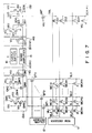
- FIG. 7 there is shown a circuit diagram of a circuit arrangement for data-sensing of an EPROM using floating gate MOSFETs as already mentioned in the prior art description, to which a semiconductor memory device according to the present invention is applied.
- MC11, MC12, ..., MC1n, ..., MCmn designate floating gate MOSFETs; DC1, DC2, ..., DCm dummy cells (first dummy cells) as floating gate MOSFETs; WL1, WL2, ..., WLm row lines; BL1, BL2, ...., BLn column lines; DBL a dummy column line; 11 a row decoder; 12 a column decoder; BT1, BT2, .., BTn column gate MOSFETs for column selection; DBT a MOSFET that is equivalent to the column gate MOSFET and is normally in a conductive state with application of a power voltage Vcc to the gate of the MOSFET; 13A a first bias setting circuit made up of n-channel MOSFETs QM1 to QM6; 14A a first load circuit made up of a p-channel MOSFET QM7; 13B a second bias setting circuit made up of n-channel MOSFETs;
- the dummy cell DC that is any one of the dummy cells DC1 to DCm comprises a MOSFET equivalent to that of a memory cell MC that is any one of the memory cells MC11 to MCmn.
- the dummy cell DCm+1 also comprises a MOSFET equivalent to that of the memory cell MC.
- the drains of them are connected together to the dummy column line DBL.
- the control gates of them are connected to the row lines WL1 to WLm, respectively.
- the sources of those transistors are grounded.
- the drain of the dummy cell DCm+1 is connected to the dummy column line DBL.
- a power voltage Vcc is always supplied to the control gate of the dummy cell DCm+1. The source thereof is grounded.
- the first and second bias potential setting circuit 13A and 13B are constructed like those in the conventional semiconductor memory device.
- the source-drain currnet path of the MOSFET QM1 is inserted between a connection point of the column gate MOSFETs BT1 to BTn and the node A.
- the gate of the MOSFET QM1 is applied with a DC bias potential V1 which is lower than the power voltage Vcc and formed by the two MOSFETs QM2 and QM3.
- the source-drain current path of the MOSFET QM4 is inserted between a connection point of the column gate MOSFETs BT1 to BTn and the power voltage Vcc.
- the gate of the MOSFET QM4 is applied with a DC bias potential V2 which is lower than the DC bias potential V1 and formed by the two MOSFETs QM5 and QM6.
- the DC bias potential V2 is set at a value which is the sum of a column line potential when a memory cell whose threshold voltage is set at a low voltage is selected and a predetermined current flows through the source-drain current path of the memory cell, and a threshold voltage of the n-channel MOSFET containing an increased threshold voltage cue to a substrate bias effect.
- the circuit arrangement of the second bias potential setting circuit 13B is substantially the same as that of the first bias potential setting circuit when the MOSFETs QD1 to QD6 are replaced by the MOSFETs QM1 to QM6.
- the first and second load circuits 14A and 14B are also substantially the same as those in the conventional memory device.
- the source-drain current path of MOSFET QM7 is inserted between the node A and the power source Vcc.
- the gate of the MOSFET QM7 is connected to its drain and the node A.
- the MOSFET QM4 in the first bias potential setting circuit 13A is for the initial charging of the column line.
- the DC bias voltage V2 is set such that the MOSFET QM4 is turned off when the column line potential exceeds a column potential when a predetermined current flows into the memory cell.
- the circuit arrangement of the second load circuit 14B is substantially the same as that in the conventional memory device. However, the conduction resistance is set smaller than that in the conventional device.
- the dummy column line DBL is connected to the dummy cell DCm+1, which constantly receives at the gate the power voltage Vcc, and normally in an on state. And, the dummy column line DBL is discharged through the dummy cell DCm+1 and a dummy cell DC (indicates any one of the dummy cells DC1 to DCm) connected to the selected row line WL.
- the conduction resistance of the load MOSFET QD7 in the second load circuit 14B is set to be approximately two times smaller than that of the MOSFET QD7 in the conventional memory device shown in Fig. 1.
- memory cells storing "1" data that are selected by switching one row line to other row line are successively subjected to a date read operation.
- the current flowing through the dummy cell DC at the time of this row line switching is shown by a curve of a one-clot-chain line in Fig. 8B.
- the value "x" of the current equals to the current flowing through the selected dummy cell DC when the potential of the selected row line is the power source voltage Vcc.
- the dummy cells DC and DCm+1 are formed of a floating gate type MOS transistor which are the same in structure, channel width, and channel length as that of the memory cell in the memory matrix.
- the current flowing through the dummy cell DCm+1 whose control gate is continuously supplied with the power source Vcc equals to the value "x". Consequently, the current flowing through the dummy cell DCm+1 also becomes the value "x" and thus, the current flowing through the dummy cells (DC and DCm+1), before the row lines are switched becomes "2x".
- the minimum value of the current flowing through the selected dummy cell DC at the row line switching is denoted by "y" in Fig. 8B. Therefore, the minimum value of the current flowing through all the dummy cells at the row line switching is "x ⁇ y".
- a solid line indicates a variation of the sum of the currents flowing through all the dummy cells.
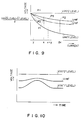
- Fig. 9 shows a variation of the reference potential Vref (indicated by a solid line) against the sum of the currents flowing through all the dummy cells, which is prepared on the basis of the Fig. 8 data.
- the illustration of Fig. 9 contains potential variations of an input potential Vin ("1" level) when the data is read out from the memory cell storing "1" data against the currents flowing through memory cell, an input potential Vin ("0" level) when the data is read out from the memory cell storing "0" data, and a reference potential Vref in the conventional memory device of Fig. 1 (indicated by a one-dot-chain line) against the current flowing through the dummy cell.
- the input potential Vin ("0" level) is constant since no current flows through the dummy cells when "0" data is read out.
- the dummy column line DBL is connected to the dummy cell DC driven by the selected row line and the dummy cell DCm+1 driven by power source Vcc. Because of this, the conduction resistance of the MOSFET QD7 in the second load circuit 14B is selected such that when a double cell current flows, the same reference potential as that of the conventional memory device can be obtained.
- the reference potential Vref of the conventional memory device of Fig. 1 reaches ⁇ (Vin ("0" level) - Vin ("1" level) ⁇ /2 at point P1 where the current flowing through the dummy cell is "x".
- the conduction resistance of MOSFET QD7 is set such that the reference potential Vref reaches ⁇ (Vin ("0" level) - Vin ("1" level) ⁇ /2 at point P2 where the current is 2x.
- the current flowing through the dummy cell becomes minimum (a point where the current is "y") at the time of the row line switching.
- the reference potential Vref rises to the potential at point P4 in the conventional memory device of Fig. 1.
- the reference potential Vref rises to reach just the potential at point P5, since the current flowing through the dummy cells is "x + y".
- Fig. 10 there are shown variations of the reference potentials Vref and the input potential Vin when the row lines are switched and the memory cells storing "1" data on the new row line is subjected to the data read operation, subsequent to the memory cells on the previous row line.
- the degree of the increase of a potential level of the reference potential Vref is much lower when compared with the degree of the increase of the reference voltage Vref in the conventional memory device of Fig. 3 (see Fig. 4).
- the curve of the reference potential Vref never crosses the line of the input potential Vin in the memory device. Therefore, the occurrence of the power source noise due to the operation of the output buffer is prevented.
- the reading speed is higher than that of the conventional device by such an amount of time T2 (Fig. 11) that a rising speed of the reference potential (indicated by a one-dot-chain line) in the present embodiment is lower than that of the reference potential (indicated by a broken line) in the conventional semiconductor device. This contributes to improvement of the data read speed.
- the power voltage Vcc is applied to the gate of the dummy cell DCm+1 for adjusting the reference potential, but it may be any other voltage than the voltage Vcc, provided that it is constant when the row lines are switched.
- the dummy cells DC1 to DCm and the dummy cell DCm+1 are connected to the same dummy column line DBL.
- Two different dummy column lines may be provided and be connected to the dummy cells DC1 to DCm, and the dummy cell DCm+1, respectively.
- each dummy column line is coupled with a MOSFET equivalent to the column gate MOSFET, and a load circuit.
- the load circuits coupled with these dummy column lines produce output signals which are supplied to an input of the sense amplifier 15.
- FIG. 12 Another embodiment of a semiconductor memory device according to the present invention will be described with reference to Fig. 12. Also in this embodiment, the present invention is applied into an EPROM using floating gate MOSFETs as memory cells.
- the present embodiment is different from the embodiment of Fig. 7 in the following points.
- An address transition detector (ATD) 18 is additionally used. An output signal of the ATD 18 is applied to the gate of the dummy cell DCm+1. In the Fig. 7 embodiment, the power voltage Vcc is constantly applied to the same.
- a row address is applied to the row address buffer 17. When a row address changes and the word lines are switched, the ATD 18 generates a pulse signal of a predetermined pulse width.
- reference numeral 19 designates a column address buffer receiving a column address.
- the output signals of the address buffers 17 and 19 are applied to the row and column decoders 17 and 19, respectively.
- the ATD 18 produces a pulse signal to turn on the dummy cell.
- the dummy cell is turned on during the time of the row line switching. Accordingly, at the time of the row line switching, a current flowing into the dummy column line DBL increases, to hold back a rise of the reference potential Vref.
- the conduction resistance of the load MOSFET QD7 in the second load circuit 14B is set at a value comparable to that of the MOSFET QD7 in the conventional semiconductor device.
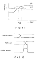
- Fig. 13 shows a timing chart for explaining the operation of the ATD 18 that is used in the embodiments of Fig. 12.
- a row address signal externally applied changes, and with the change of the address signal, the row line currently used is switched to a new row line.
- the ATD 18 produces a pulse signal which retains a "1" logical state during this period.
- a circuit having such a function may readily be realized by combining signal delay and logic circuits.
- the present invention is applicable not only for the EPROM but also for a mask ROM using MOSFETs of a single gate structure as memory cells, whose threshold voltages are adjusted, low and high, by selectively doping impurity into the channel regions of the transistors during the manufacturing process.
Landscapes
- Read Only Memory (AREA)
- Static Random-Access Memory (AREA)
Description
- The present invention relates to a semiconductor memory device improved in a reference potential generating circuit for a sense amplifier and load circuits for memory cells.
- From EP-A-0 270 750 which discloses the features of the preamble of
claims - The technical background of the present invention will be described in the following by reference to a conventional semiconductor memory device.
- Such a conventional semiconductor memory device shown in Fig. 1 is an erasable and programmable ROM (EPROM) using floating gate MOSFETs as memory cells.
- In the Figure, MC11, MC12, ..., MC1n designate floating gate MOSFETs; DC a floating gate MOSFET as a dummy cell; WL1, WL2, ..., WLm row lines; BL1, BL2, ..., BLn column lines; DBL a dummy column line; 11 a row decoder; 12 a column decoder; BT1, BT2, ..., BTn column gate MOSFETs for column selection; DBT a MOSFET that is equivalent to the column gate MOSFET and is normally in a conductive state with application of a power voltage Vcc to the gate of the MOSFET; 13A a first bias setting circuit made up of n-channel MOSFETs QM1 to QM6; 14A a first load circuit made up of a p-channel MOSFET QM7; 13B a second bias setting circuit made up of n-channel MOSFETs QD1 to QD6; 14B a second load circuit made up of a p-channel MOSFET QD7; 15 a sense amplifier; and 16 an output buffer.
- In the description to follow, MOSFETs whose channels are not specified will be treated as n-channel MOSFETs.
- The dummy cell DC consists of a MOSFET equivalent to that of a memory cell MC that is any of the memory cells MC11 to MCmn. The dummy column line DBL is equivalent to the column line BL that is any of those column lines BL1 to BLn.
- A potential V1 at the output node of a low potential generating circuit formed of MOSFETs QM2 and QM3, which is lower than the power voltage Vcc, is applied to the gate of a MOSFET QM1 in the first
bias setting circuit 13A. A potential V2 at the output node of a low potential generating circuit formed of MOSFETs QM5 and QM6, which is lower than the node potential V1, is applied to the gate of a MOSFET QM4. The node potential V2 is set a a voltage which is the sum of a potential on the column line BL when a Predetermined current flows into the memory cell MC, and a threshold voltage of the n-channel MOSFET containing an increased threshold voltage due to the substrate bias effect. The MOSFET QM4 is an initial charging MOSFET for quickening an initial charging to the column line BL in which the column line BL is charged from an initial voltage 0 V. The initial charging MOSFET is rendered nonconductive when the column line potential exceeds a potential on the column line when a predetermined current flows into the memory cell MC. - In the EPROM thus arranged, a reference potential Vref is generated by the
second load circuit 14B on the basis of the data in the dummy cell DC, and appears at a node B. An input potential Vin is generated by thefirst load circuit 14A on the basis of the data read out of a memory cell MC as selected by the output signals of the row decoder 11 and thecolumn decoder 12, and appears at a node A. Thesense amplifier 15 compares the reference potential Vref and the input potential Vin to sense a type of the data stored in the memory cell MC. The sensed data is amplified by thesense amplifier 15, and outputted through theoutput buffer 16. - In each memory cell of the EPROM, data is programmed by selectively injecting electrons into the floating gate of the cell. For injecting electrons into the floating gate, a high voltage, e.g., 12.5 to 21 V, which is much higher than the normal power voltage, e.g., 5 V, is applied to the column line and row lines as are selected by the row decoder 11 and the
column decoder 12. Under such a high voltage, an impact ionization occurs in the vicinity of the drain of the memory cell located at a cross point of the selected row and column lines, to generate electron-hole pairs. Of the generated electron-hole pairs, the electrons are injected into the floating gate of the memory cell. A threshold voltage of the memory cell injected with electrons is much higher than that of the memory cell not injected. The memory cell whose floating gate is injected with electrons maintains an off-state even if a signal of "1" level (power voltage Vcc) is supplied to the control gate of the cell, or the row line. Under the same condition, the memory cell not injected with electrons is turned on. Since the dummy cell DC is not injected with electrons, no potential difference is caused between the potentials Vref and Vin. - To avoid this, a channel width WD7 of the MOSFET QD7 in the
second load circuit 14B is set to be larger than that WM7 of the MOSFET QM7 in thefirst load circuit 14A. With such a channel width selection, a conduction resistance of the MOSFET QD7 is smaller than that of the MOSFET QM7. To be more specific, the conduction resistance of the MOSFET QD7 is so selected that the reference potential Vref is between the Vin potential when the electron injected memory cell is selected and the Vin potential when the no electron injected memory cell is selected. With such an arrangement, even when the no electron injected memory cell is selected, a preset potential difference is caused between the potentials Vref and Vin. When the selected memory cell is an electron injected one, the potential Vin represents a potential which is the result of a subtraction of the threshold voltage of the load MOSFET QM7 from the power source voltage Vcc. - In the subsequent description, the electron injected memory cell or the memory cell with a high threshold level will be assumed to be a memory cell storing "0" data. The no electron injected memory cell or the memory cell with a low threshold voltage will be assumed to be a memory cell storing "1" data.
- In the above EPROM, the data read out by the sense amplifier is received by the
buffer 16, and thebuffer 16 outputs the data. In theoutput buffer 16, it is necessary to charge and discharge an external large load capacitor. Therefore, when theoutput buffer 16 produces the data, noise is generated in the power source. The noise causes a variation in the power source voltage Vcc. As recalled, the conduction resistance of the MOSFET QD7 in thesecond load circuit 14B is different from that of the MOSFET QM7 in thefirst load circuit 14A. Therefore, these transistors respond to the power voltage variation in a different way. In an extreme case, a proper amplitude relationship between the potentials Vin and Vref is reversed, so that the sense amplifier may produce erroneous data. Such a malfunction of the sense amplifier should be avoided. - The EPROM of Fig. 1 will encounter a situation that a row line connected to the memory cells of "1" data that is currently selected is switched to another row line connected to the memory cell having the same data, and subsequently the data are successively read out from the memory cells on the new row.
- In such a situation, the memory cells selected anew are insufficiently turned on in the initial stage, until the potential of the row line selected anew reaches power source voltage Vcc. Consequently, the potential of the selected bit line is temporarily increased. The threshold voltage of the memory cell of the floating gate structure is approximately 2 V. During the transient period of time that the row lines are switched one from the other, the memory cells connected to the selected column line are instantaneously in an off-state. Because of this, at the time of switching the row lines, there occurs a charging operation for the column line, and the potential Vin of the node A temporarily rises, as shown in Fig. 2.
- Meanwhile, since the dummy cell DC is placed always in an on state by the power voltage Vcc, the reference potential Vref is always constant as shown in Fig. 2 showing waveforms of potentials Vref and Vin. When the potential Vin rises and crosses a line of the reference potential Vref as shown, the
sense amplifier 15 temporarily produces the data of an improper logic level. As a result, the output data of thebuffer 16 varies its logic level, "1" → "0" → "1", during a short period. Therefore, an inductance component existing in the lead creates a great variation of the earth voltage, possibly causing a malfunction of a circuit in the EPROM. - To prevent the malfunction of the circuit due to a variation of the earth voltage, there has been proposed an EPROM as shown in Fig. 3.
- In this EPROM, the dummy cells DC1 to DCm are provided corresponding to row lines WL1 to WLm, respectively. The control gates of the dummy cells DC1 to DCm are connected to the row lines WL1 to WLm, respectively. And, the drains of the dummy cells DC1 to DCm are connected to a dummy column line DBL.
- In the arrangement of the EPROM, the dummy cells are controlled by the signals on the row lines. Even in the situation that the row lines are switched from one to the other, and succeeding to the memory cell storing data "1" on the previous or old row line, the memory cell storing the data "1" on the present or new row line are subjected to the read operation, the dummy column line DBL is charged by the
load circuit 14B at the time of switching the row lines. Accordingly, as seen from Fig. 4 showing waveforms, the reference potential Vref rises as the potential Vin ("1" level) rises. In the EPROM, the potential Vin does not cross the curve of the reference potential Vref. The output data of theoutput buffer 16 is invariable, and no variation of the earth voltage is caused. - The rise of the potentials Vin and Vref is caused by the charging operation at the time of switching of the row lines, and hence the degree of the potential rise is different dependent on the conduction resistances of the MOSFETs QM7 and QD7 in the
load circuits - As described above, in a conventional semiconductor memory device, when the row lines are switched under the condition that a memory cell storing "1" data is selected to select a memory cell storing "1" data, error data is outputted, and a noise occurs in the power source to consequently cause a malfunction of the semiconductor memory device.
- In another conventional semiconductor memory device solving the above problem, a variation of the reference potential is greater than that of the input potential. Therefore, the data reading speed when the selected row line is switched becomes slow.
- A characteristic curve depicted by a solid line in Fig. 6 shows a voltage vs. current characteristic curve of the
first load circuit 14A in the conventional semiconductor memory device. In the figure, the abscissa represents a potential Vin at the node A and the ordinates a load current flowing into the load circuit. It is assumed that Vin ("1" level) is a potential at the node A caused when the memory cell of a low threshold voltage is selected and a memory cell current Icell flows, and Vin ("0" level) is a potential at the node A and Vref is a potential at the node B. - It has been known that the time required for the row line selection and the time required for the charging or discharging of the junction capacitance connected to the column line greatly determine a data read speed of a nonvolatile semiconductor memory device of the structure shown in Fig. 1. A signal delay time in the row line depends largely on a resistance of the material of the row line. For this reason, tungsten silicide has recently superseded polysilicon used conventionally. The resistance of tungsten silicide is smaller than that of polysilicon. As a result, the data read speed depends largely on the charging and discharging speed of the junction capacitance connected to the column line. Particularly, when the column line is switched one from the other, and the memory cell of a high threshold voltage is selected, the charging to the new selected column line starts at the voltage of 0 V. Capacitance connected to the column lines has become large, with the increase of the semiconductor memory capacity. Accordingly, to realize a high speed read operation, it is necessary to quicken both the charging speed of the column line and the read operation for reading out the "0" data. In conventional measures taken for this, the column line is charged at a high speed through the initial charging transistor QM4 when the potential is less than Vin ("1" level). When the potential of the column line BL exceeds Vin ("1" level), the transistor QM4 becomes nonconductive. At this time, only the p-channel transistor QM7 in the
load circuit 14A charges the column line BL. Since the gate of the p-channel transistor QM7 is connected to the drain thereof, when the potential Vin at the node A rises, a conduction resistance of this transistor QM7 rapidly increases, and a charge current rapidly decreases. Therefore, it takes much time for the potential at the node A to rise from Vin ("1" level) to Vin ("0" level), lowering the data read speed. In other words, the time taken for the node A potential to rise from Vin ("1" level) to Vin ("0" level) can be reduced by increasing the channel width of the transistor QM7 and reducing its conduction resistance. However, the decrease of the conduction resistance of the transistor QM7 creates another problem that a margin for the power source noise is narrowed. - In Fig. 6, a characteristic curve as indicated by a dotted line is obtained for the transistor QM7 whose conduction resistance is 1/2 that of the same transistor when the cell current vs. input voltage Vin characteristic thereof is indicated by a solid line. When the 1/2 conduction resistance of the transistor QM7 is set, the potential Vin at the node A when the memory cell storing the "1" data, viz., the memory cell of a low threshold voltage, is selected, is Vin ("1" level)′. The potential Vref′ at the node B is set at exactly the middle point between the potential Vin ("1" level)′ at the node A when the memory cell of "1" data is selected and that Vin ("0" level) when the memory cell storing "0" data, i.e., the memory cell of a low threshold voltage. Accordingly, the conduction resistance of the p-channel MOS transistor QD7 in the
second load circuit 14B is so selected that the potential at node B when the 1/2 conduction resistance of transistor QM7 is set, is equal to Vref′ as {Vin ("0" level) - Vin("1" level)}/2. As a result, when the data of "1" or "0" is selected, a difference between the potential at the node B and that at the node A is reduced by {Vin ("1" level)′ - Vin ("1" level)}/2. Generally, the ground potential greatly varies when the data is outputted from the output buffer. At this time, the potentials at the nodes A and B also vary due to the ground potential variation. In the first andsecond load circuits - As described above, in the conventional semiconductor memory device improved in the read speed by using a small conduction resistance in the load circuit, the semiconductor memory device is apt to malfunction due to the power noise.
- Accordingly, an object of the present invention is to provide a semiconductor memory device which is free from the power noise even during a transient period that row lines are switched from one to the other, and is operable at an increased data read speed.
- According to the present invention that it directed to achieve the above object, there is provided a semiconductor memory device comprising the features of
independent claims - In semiconductor memory devices thus arranged, the second dummy cell, which is set in an on state normally or during a transient period of switching row lines from one to the other, is connected to the dummy column line. The connection of the second dummy cell with the dummy line changes a current flowing to the dummy line at the time of row line switching, thereby to hold back a rise of the reference potential at the time of the row line switching.
- This invention can be more fully understood from the following detailed description when taken in conjunction with the accompanying drawings, in which:
- Fig. 1 is a circuit diagram of a conventional semiconductor memory device;
- Fig. 2 shows a graphical representation of transient voltage waveforms at the nodes A and B in the memory device shown in Fig. 1;
- Fig. 3 is a circuit diagram of another conventional semiconductor memory device;
- Figs. 4 and 5 show graphical representations of transient voltage waveforms at the nodes A and B in the memory device shown in Fig. 3;
- Fig. 6 shows a graphical representation of a load current vs. sensing node voltage characteristic of a first load circuit in the conventional memory device;
- Fig. 7 is a circuit diagram of a semiconductor memory device according to an embodiment of the present invention;
- Figs. 8A and 8B, 9 to 11 are graphs showing operation characteristics of the semiconductor memory device of Fig. 7;
- Fig. 12 are circuit diagrams of a semiconductor memory device according to an other embodiment of the present invention;
- Fig. 13 shows a set of waveforms of signals in an address transition detector used in the embodiment of Fig. 12;
- Some specific embodiments of a semiconductor device according to the present invention will be described with reference the accompanying drawings.
- Referring now to Fig. 7, there is shown a circuit diagram of a circuit arrangement for data-sensing of an EPROM using floating gate MOSFETs as already mentioned in the prior art description, to which a semiconductor memory device according to the present invention is applied.
- In Fig. 7, MC11, MC12, ..., MC1n, ..., MCmn designate floating gate MOSFETs; DC1, DC2, ..., DCm dummy cells (first dummy cells) as floating gate MOSFETs; WL1, WL2, ..., WLm row lines; BL1, BL2, ...., BLn column lines; DBL a dummy column line; 11 a row decoder; 12 a column decoder; BT1, BT2, .., BTn column gate MOSFETs for column selection; DBT a MOSFET that is equivalent to the column gate MOSFET and is normally in a conductive state with application of a power voltage Vcc to the gate of the MOSFET; 13A a first bias setting circuit made up of n-channel MOSFETs QM1 to QM6; 14A a first load circuit made up of a p-channel MOSFET QM7; 13B a second bias setting circuit made up of n-channel MOSFETs QD1 to QD6; 14B a second load circuit made up of a p-channel MOSFET QD7; 15 a sense amplifier; and 16 an output buffer.
- In the description to follow, MOSFETs whose channels are not specified will be treated as n-channel MOSFETs. The dummy cell DC that is any one of the dummy cells DC1 to DCm comprises a MOSFET equivalent to that of a memory cell MC that is any one of the memory cells MC11 to MCmn. The dummy cell DCm+1 also comprises a MOSFET equivalent to that of the memory cell MC.
- In the dummy cells DC1, DC2, ..., DCm, the drains of them are connected together to the dummy column line DBL. The control gates of them are connected to the row lines WL1 to WLm, respectively. The sources of those transistors are grounded. The drain of the dummy cell DCm+1 is connected to the dummy column line DBL. A power voltage Vcc is always supplied to the control gate of the dummy
cell DCm+ 1. The source thereof is grounded. - The first and second bias
potential setting circuit - For example, in the first bias
potential setting circuit 13A, the source-drain currnet path of the MOSFET QM1 is inserted between a connection point of the column gate MOSFETs BT1 to BTn and the node A. The gate of the MOSFET QM1 is applied with a DC bias potential V1 which is lower than the power voltage Vcc and formed by the two MOSFETs QM2 and QM3. The source-drain current path of the MOSFET QM4 is inserted between a connection point of the column gate MOSFETs BT1 to BTn and the power voltage Vcc. The gate of the MOSFET QM4 is applied with a DC bias potential V2 which is lower than the DC bias potential V1 and formed by the two MOSFETs QM5 and QM6. The DC bias potential V2 is set at a value which is the sum of a column line potential when a memory cell whose threshold voltage is set at a low voltage is selected and a predetermined current flows through the source-drain current path of the memory cell, and a threshold voltage of the n-channel MOSFET containing an increased threshold voltage cue to a substrate bias effect. - The circuit arrangement of the second bias
potential setting circuit 13B is substantially the same as that of the first bias potential setting circuit when the MOSFETs QD1 to QD6 are replaced by the MOSFETs QM1 to QM6. - The first and
second load circuits - Specifically, in the
first load circuit 14A, the source-drain current path of MOSFET QM7 is inserted between the node A and the power source Vcc. The gate of the MOSFET QM7 is connected to its drain and the node A. The MOSFET QM4 in the first biaspotential setting circuit 13A is for the initial charging of the column line. When a column line BL is selected and a charging for the column line BL starts from an initial value 0 V, the transistor QM4 quickens the initial charging. The DC bias voltage V2 is set such that the MOSFET QM4 is turned off when the column line potential exceeds a column potential when a predetermined current flows into the memory cell. - The circuit arrangement of the
second load circuit 14B is substantially the same as that in the conventional memory device. However, the conduction resistance is set smaller than that in the conventional device. The dummy column line DBL is connected to the dummycell DCm+ 1, which constantly receives at the gate the power voltage Vcc, and normally in an on state. And, the dummy column line DBL is discharged through the dummy cell DCm+1 and a dummy cell DC (indicates any one of the dummy cells DC1 to DCm) connected to the selected row line WL. Accordingly, to maintain the reference potential Vref at the mid potential between "1" and "0" level of the input potential Vin, the conduction resistance of the load MOSFET QD7 in thesecond load circuit 14B is set to be approximately two times smaller than that of the MOSFET QD7 in the conventional memory device shown in Fig. 1. - The operation of the semiconductor memory device thus arranged will be described.
- In the operation, memory cells storing "1" data that are selected by switching one row line to other row line are successively subjected to a date read operation. When the row lines are switched, as shown in Fig. 8A showing waveforms, a potential of the non-selected row line WLi (i = 1, 2, ..., m) drops from "1" to "0" in level. A potential of the selected row line WLj (j =1, 2, ..., m) rises from a "0" level to "1". The current flowing through the dummy cell DC at the time of this row line switching, is shown by a curve of a one-clot-chain line in Fig. 8B. In the figure, the value "x" of the current equals to the current flowing through the selected dummy cell DC when the potential of the selected row line is the power source voltage Vcc. In this embodiment, the dummy cells DC and DCm+1 are formed of a floating gate type MOS transistor which are the same in structure, channel width, and channel length as that of the memory cell in the memory matrix. Also in this embodiment, the current flowing through the dummy cell DCm+1 whose control gate is continuously supplied with the power source Vcc equals to the value "x". Consequently, the current flowing through the dummy cell DCm+1 also becomes the value "x" and thus, the current flowing through the dummy cells (DC and DCm+1), before the row lines are switched becomes "2x".
- The minimum value of the current flowing through the selected dummy cell DC at the row line switching is denoted by "y" in Fig. 8B. Therefore, the minimum value of the current flowing through all the dummy cells at the row line switching is "x ÷ y". In Fig. 8B, a solid line indicates a variation of the sum of the currents flowing through all the dummy cells.
- Fig. 9 shows a variation of the reference potential Vref (indicated by a solid line) against the sum of the currents flowing through all the dummy cells, which is prepared on the basis of the Fig. 8 data. In addition to the reference potential Vref, the illustration of Fig. 9 contains potential variations of an input potential Vin ("1" level) when the data is read out from the memory cell storing "1" data against the currents flowing through memory cell, an input potential Vin ("0" level) when the data is read out from the memory cell storing "0" data, and a reference potential Vref in the conventional memory device of Fig. 1 (indicated by a one-dot-chain line) against the current flowing through the dummy cell. The input potential Vin ("0" level) is constant since no current flows through the dummy cells when "0" data is read out.
- In the present embodiment, the dummy column line DBL is connected to the dummy cell DC driven by the selected row line and the dummy cell DCm+1 driven by power source Vcc. Because of this, the conduction resistance of the MOSFET QD7 in the
second load circuit 14B is selected such that when a double cell current flows, the same reference potential as that of the conventional memory device can be obtained. - As seen from the graph, the reference potential Vref of the conventional memory device of Fig. 1 reaches {(Vin ("0" level) - Vin ("1" level)}/2 at point P1 where the current flowing through the dummy cell is "x". In the memory device of the present embodiment, the conduction resistance of MOSFET QD7 is set such that the reference potential Vref reaches {(Vin ("0" level) - Vin ("1" level)}/2 at point P2 where the current is 2x.
- In the memory device under discussion having such a Vref variation, the current flowing through the dummy cell becomes minimum (a point where the current is "y") at the time of the row line switching. When the potential Vin ("1" level) rises to the potential at point P3, the reference potential Vref rises to the potential at point P4 in the conventional memory device of Fig. 1. On the other hand, in the semiconductor device according to the present invention, the reference potential Vref rises to reach just the potential at point P5, since the current flowing through the dummy cells is "x + y".
- Turning now to Fig. 10, there are shown variations of the reference potentials Vref and the input potential Vin when the row lines are switched and the memory cells storing "1" data on the new row line is subjected to the data read operation, subsequent to the memory cells on the previous row line. As seen from the graph, when the current flowing through the dummy cell becomes minimum at the time of the row line switching, the degree of the increase of a potential level of the reference potential Vref is much lower when compared with the degree of the increase of the reference voltage Vref in the conventional memory device of Fig. 3 (see Fig. 4). Further, the curve of the reference potential Vref never crosses the line of the input potential Vin in the memory device. Therefore, the occurrence of the power source noise due to the operation of the output buffer is prevented.
- When the row lines are switched one from the other, and the memory cell from which data is read out is shifted from the "1" memory cell to a "0" memory cell, the reading speed is higher than that of the conventional device by such an amount of time T2 (Fig. 11) that a rising speed of the reference potential (indicated by a one-dot-chain line) in the present embodiment is lower than that of the reference potential (indicated by a broken line) in the conventional semiconductor device. This contributes to improvement of the data read speed.
- In the embodiment of Fig. 7, the power voltage Vcc is applied to the gate of the dummy cell DCm+1 for adjusting the reference potential, but it may be any other voltage than the voltage Vcc, provided that it is constant when the row lines are switched. Also in the above embodiment, the dummy cells DC1 to DCm and the dummy cell DCm+1 are connected to the same dummy column line DBL. Two different dummy column lines may be provided and be connected to the dummy cells DC1 to DCm, and the dummy
cell DCm+ 1, respectively. In this case, each dummy column line is coupled with a MOSFET equivalent to the column gate MOSFET, and a load circuit. The load circuits coupled with these dummy column lines produce output signals which are supplied to an input of thesense amplifier 15. The same effects as those in the above embodiment are provided in this modification. - Another embodiment of a semiconductor memory device according to the present invention will be described with reference to Fig. 12. Also in this embodiment, the present invention is applied into an EPROM using floating gate MOSFETs as memory cells. The present embodiment is different from the embodiment of Fig. 7 in the following points. An address transition detector (ATD) 18 is additionally used. An output signal of the
ATD 18 is applied to the gate of the dummycell DCm+ 1. In the Fig. 7 embodiment, the power voltage Vcc is constantly applied to the same. A row address is applied to therow address buffer 17. When a row address changes and the word lines are switched, theATD 18 generates a pulse signal of a predetermined pulse width. - Incidentally,
reference numeral 19 designates a column address buffer receiving a column address. The output signals of the address buffers 17 and 19 are applied to the row andcolumn decoders - In this embodiment, during a transient period that a row address changes and the present row line is switched to another row line, the
ATD 18 produces a pulse signal to turn on the dummy cell. In other words, the dummy cell is turned on during the time of the row line switching. Accordingly, at the time of the row line switching, a current flowing into the dummy column line DBL increases, to hold back a rise of the reference potential Vref. - In this embodiment, during the time other than the transient time of the row line switching, the dummy cell DCm+1 is turned off. Accordingly, the conduction resistance of the load MOSFET QD7 in the
second load circuit 14B is set at a value comparable to that of the MOSFET QD7 in the conventional semiconductor device. - In each of the above embodiments, at the time of the row line switching, to hold back a rise of the reference potential Vref at the time of the row line switching, the discharge current of the dummy column line DBL is increased.
- Fig. 13 shows a timing chart for explaining the operation of the
ATD 18 that is used in the embodiments of Fig. 12. As seen from the timing chart, a row address signal externally applied changes, and with the change of the address signal, the row line currently used is switched to a new row line. During this period of the row line switching, theATD 18 produces a pulse signal which retains a "1" logical state during this period. A circuit having such a function may readily be realized by combining signal delay and logic circuits. - It is evident that the present invention is applicable not only for the EPROM but also for a mask ROM using MOSFETs of a single gate structure as memory cells, whose threshold voltages are adjusted, low and high, by selectively doping impurity into the channel regions of the transistors during the manufacturing process.
- As seen from the foregoing description, in the memory device according to each of the above-mentioned embodiments, a rise of the reference potential Vref is held back even during the time of the row line switching. Accordingly, no noise is entered into the power source. A data read speed of the memory device is improved.
Claims (4)
- A semiconductor memory device comprising:
memory cells (MC11, ..., MCmn);
column lines (BL1, ..., BLn) receiving data from said memory cells;
a first load circuit (14A) coupled with said column lines;
first dummy cells (CD1, ..., DCm);
a dummy column lines (DBL) to which said first dummy cells are connected;
a second load circuit (14B) connected to said dummy column line;
a second dummy cell (DCm+1) connected to said dummy column line and supplied at the gate with a predetermined potential; and
a sense amplifier (15) for sensing the data stored in said memory cell in accordance with a potential difference between said column line and said dummy column line;
row lines (WL1, ..., WLm) and a row decoder for selecting said memory cells, connected to said memory cells and said first dummy cells through the row lines;
said memory cells (MC11, ..., MCmn) are selected by said row decoder; and
said first dummy cells (DC1, ..., DCm) are selected by said row decoder, each of the first dummy cells having a control gate connected to a corresponding one of said row lines;
characterized in that
said second dummy cell (DCm+1) sets a voltage on said dummy column line to become lower than a voltage on said column line when all of said memory cells and all of said first dummy cells are non-selected. - A semiconductor memory device comprising:
memory cells (MC11, ..., MCmn);
column lines (BL1, ..., BLn) receiving data from said memory cells;
a first load circuit (14A) coupled with said column lines;
first dummy cells (DC1, ..., DCm);
a dummy column line (DBL) to which said first dummy cells are connected;
a second load circuit (14B) connected to said dummy column line;
a second dummy cell (DCm+1) conected to said dummy column line;
a sense amplifier (15) for sensing the data stored in said memory cell in accordance with a potential difference between said column line and said dummy column line,
row lines (WL1, ..., WLm);
said memory cells (MC11, ..., MCmn) are selected by said row lines; and
said first dummy cells (DC1, ..., DCm) are selected by said row lines;
characterized by
a pulse signal generating circuit (18) for generating a pulse signal by detecting a change in an address input signal;
said second dummy cell (DCm+1) receives at the gate the pulse signal generated by said pulse signal generating circuit and is controlled by the pulse signal so that a voltage on said dummy column line becomes lower than a voltage on said column line when all of said memory cells and all of said first dummy cells are non-selected. - A semiconductor memory device according to claim 1, characterized in that said predetermined potential is a power source voltage.
- A semiconductor memory device according to claim 1, characterized in that said predetermined potential is a potential different from a power source voltage.
Priority Applications (2)
| Application Number | Priority Date | Filing Date | Title |
|---|---|---|---|
| EP93114324A EP0576046B1 (en) | 1988-06-24 | 1989-06-23 | Semiconductor memory device |
| EP93114322A EP0576045B1 (en) | 1988-06-24 | 1989-06-23 | Semiconductor memory device |
Applications Claiming Priority (4)
| Application Number | Priority Date | Filing Date | Title |
|---|---|---|---|
| JP156539/88 | 1988-06-24 | ||
| JP15653988A JPH07109719B2 (en) | 1988-06-24 | 1988-06-24 | Semiconductor memory device |
| JP161344/88 | 1988-06-29 | ||
| JP16134488A JPH0642320B2 (en) | 1988-06-29 | 1988-06-29 | Semiconductor memory device |
Related Child Applications (4)
| Application Number | Title | Priority Date | Filing Date |
|---|---|---|---|
| EP93114324A Division EP0576046B1 (en) | 1988-06-24 | 1989-06-23 | Semiconductor memory device |
| EP93114322A Division EP0576045B1 (en) | 1988-06-24 | 1989-06-23 | Semiconductor memory device |
| EP93114322.6 Division-Into | 1989-06-23 | ||
| EP93114324.2 Division-Into | 1989-06-23 |
Publications (3)
| Publication Number | Publication Date |
|---|---|
| EP0347935A2 EP0347935A2 (en) | 1989-12-27 |
| EP0347935A3 EP0347935A3 (en) | 1991-05-29 |
| EP0347935B1 true EP0347935B1 (en) | 1995-07-26 |
Family
ID=26484252
Family Applications (3)
| Application Number | Title | Priority Date | Filing Date |
|---|---|---|---|
| EP93114324A Expired - Lifetime EP0576046B1 (en) | 1988-06-24 | 1989-06-23 | Semiconductor memory device |
| EP93114322A Expired - Lifetime EP0576045B1 (en) | 1988-06-24 | 1989-06-23 | Semiconductor memory device |
| EP89111475A Expired - Lifetime EP0347935B1 (en) | 1988-06-24 | 1989-06-23 | Semiconductor memory device |
Family Applications Before (2)
| Application Number | Title | Priority Date | Filing Date |
|---|---|---|---|
| EP93114324A Expired - Lifetime EP0576046B1 (en) | 1988-06-24 | 1989-06-23 | Semiconductor memory device |
| EP93114322A Expired - Lifetime EP0576045B1 (en) | 1988-06-24 | 1989-06-23 | Semiconductor memory device |
Country Status (4)
| Country | Link |
|---|---|
| US (1) | US5040148A (en) |
| EP (3) | EP0576046B1 (en) |
| KR (1) | KR930001735B1 (en) |
| DE (3) | DE68926124T2 (en) |
Families Citing this family (21)
| Publication number | Priority date | Publication date | Assignee | Title |
|---|---|---|---|---|
| US5191552A (en) * | 1988-06-24 | 1993-03-02 | Kabushiki Kaisha Toshiba | Semiconductor memory device with address transition actuated dummy cell |
| US5276643A (en) * | 1988-08-11 | 1994-01-04 | Siemens Aktiengesellschaft | Integrated semiconductor circuit |
| JPH03156795A (en) * | 1989-11-15 | 1991-07-04 | Toshiba Micro Electron Kk | Semiconductor memory circuit device |
| IT1246241B (en) * | 1990-02-23 | 1994-11-17 | Sgs Thomson Microelectronics | CIRCUIT FOR READING THE INFORMATION CONTAINED IN NON-VOLATILE MEMORY CELLS |
| DE69029968T2 (en) * | 1990-11-19 | 1997-06-05 | Sgs Thomson Microelectronics | Saving with unequal loads and with compensation |
| KR940005688B1 (en) * | 1991-09-05 | 1994-06-22 | 삼성전자 주식회사 | Automatic precharge inspection of data lines in memory devices |
| JPH0574181A (en) * | 1991-09-10 | 1993-03-26 | Nec Corp | Data readout circuit of semiconductor memory device |
| JP3397427B2 (en) * | 1994-02-02 | 2003-04-14 | 株式会社東芝 | Semiconductor storage device |
| US5390147A (en) | 1994-03-02 | 1995-02-14 | Atmel Corporation | Core organization and sense amplifier having lubricating current, active clamping and buffered sense node for speed enhancement for non-volatile memory |
| DE69424771T2 (en) * | 1994-03-22 | 2000-10-26 | Stmicroelectronics S.R.L., Agrate Brianza | Arrangement for reading a memory cell matrix |
| EP0675501B1 (en) * | 1994-03-31 | 2001-06-13 | STMicroelectronics S.r.l. | Non-volatile memory element with double programmable cell and corresponding reading circuit for redundancy circuits |
| GB9423034D0 (en) * | 1994-11-15 | 1995-01-04 | Sgs Thomson Microelectronics | A reference circuit |
| JPH08221996A (en) * | 1995-02-17 | 1996-08-30 | Nec Corp | Semiconductor storage |
| JP3734550B2 (en) * | 1996-01-30 | 2006-01-11 | 株式会社ルネサステクノロジ | Semiconductor memory device |
| EP0798740B1 (en) * | 1996-03-29 | 2003-11-12 | STMicroelectronics S.r.l. | Reference system for determining the programmed/non-programmed status of a memory cell, particularly for non-volatile memories |
| US5602788A (en) * | 1996-06-07 | 1997-02-11 | International Business Machines Corporation | Read only memory having localized reference bit lines |
| US5729493A (en) * | 1996-08-23 | 1998-03-17 | Motorola Inc. | Memory suitable for operation at low power supply voltages and sense amplifier therefor |
| EP1063654B1 (en) * | 1999-06-21 | 2003-03-05 | STMicroelectronics S.r.l. | "Reading method for non-volatile memories with sensing ratio variable with the reading voltage, and device to realize said method" |
| TW559814B (en) * | 2001-05-31 | 2003-11-01 | Semiconductor Energy Lab | Nonvolatile memory and method of driving the same |
| JP2003077282A (en) * | 2001-08-31 | 2003-03-14 | Fujitsu Ltd | Nonvolatile semiconductor memory device |
| KR100454145B1 (en) * | 2001-11-23 | 2004-10-26 | 주식회사 하이닉스반도체 | Flash memory device |
Family Cites Families (10)
| Publication number | Priority date | Publication date | Assignee | Title |
|---|---|---|---|---|
| JPS53117341A (en) * | 1977-03-24 | 1978-10-13 | Toshiba Corp | Semiconductor memory |
| DE3482724D1 (en) * | 1983-04-07 | 1990-08-23 | Toshiba Kawasaki Kk | FIXED VALUE STORAGE. |
| JPH0666115B2 (en) * | 1983-09-26 | 1994-08-24 | 株式会社東芝 | Semiconductor memory device |
| JPS60150297A (en) * | 1984-01-13 | 1985-08-07 | Nec Corp | Memory |
| US4805143A (en) * | 1986-01-16 | 1989-02-14 | Hitachi Ltd. | Read-only memory |
| JPS62197996A (en) * | 1986-02-24 | 1987-09-01 | Toshiba Corp | Sense amplifier for semiconductor memory |
| JPS62231500A (en) * | 1986-03-31 | 1987-10-12 | Toshiba Corp | Semiconductor storage device |
| US4819212A (en) * | 1986-05-31 | 1989-04-04 | Kabushiki Kaisha Toshiba | Nonvolatile semiconductor memory device with readout test circuitry |
| IT1213343B (en) * | 1986-09-12 | 1989-12-20 | Sgs Microelettronica Spa | DETECTION CIRCUIT OF THE STATE OF MATRIX CELLS IN EPROM MEMORIES IN MOS TECHNOLOGY. |
| JP2507529B2 (en) * | 1988-03-31 | 1996-06-12 | 株式会社東芝 | Nonvolatile semiconductor memory device |
-
1989
- 1989-06-23 DE DE68926124T patent/DE68926124T2/en not_active Expired - Fee Related
- 1989-06-23 EP EP93114324A patent/EP0576046B1/en not_active Expired - Lifetime
- 1989-06-23 US US07/370,869 patent/US5040148A/en not_active Expired - Lifetime
- 1989-06-23 EP EP93114322A patent/EP0576045B1/en not_active Expired - Lifetime
- 1989-06-23 DE DE68923624T patent/DE68923624T2/en not_active Expired - Fee Related
- 1989-06-23 DE DE68923588T patent/DE68923588T2/en not_active Expired - Fee Related
- 1989-06-23 EP EP89111475A patent/EP0347935B1/en not_active Expired - Lifetime
- 1989-06-24 KR KR1019890008749A patent/KR930001735B1/en not_active Expired - Fee Related
Also Published As
| Publication number | Publication date |
|---|---|
| EP0347935A3 (en) | 1991-05-29 |
| KR910001750A (en) | 1991-01-31 |
| EP0576045B1 (en) | 1995-07-26 |
| DE68923588D1 (en) | 1995-08-31 |
| DE68923624T2 (en) | 1996-02-01 |
| KR930001735B1 (en) | 1993-03-12 |
| EP0576046A2 (en) | 1993-12-29 |
| DE68926124T2 (en) | 1996-09-19 |
| EP0576046B1 (en) | 1996-03-27 |
| EP0576045A3 (en) | 1994-02-16 |
| DE68923588T2 (en) | 1996-07-04 |
| EP0347935A2 (en) | 1989-12-27 |
| EP0576045A2 (en) | 1993-12-29 |
| EP0576046A3 (en) | 1994-02-09 |
| DE68923624D1 (en) | 1995-08-31 |
| US5040148A (en) | 1991-08-13 |
| DE68926124D1 (en) | 1996-05-02 |
Similar Documents
| Publication | Publication Date | Title |
|---|---|---|
| EP0347935B1 (en) | Semiconductor memory device | |
| US6490199B2 (en) | Sense amplifier circuit for a flash memory device | |
| EP0337393B1 (en) | 2-cell/1-bit type EPROM | |
| US4884241A (en) | Nonvolatile semiconductor memory device | |
| US5748536A (en) | Data read circuit for a nonvolatile semiconductor memory | |
| US5463583A (en) | Non-volatile semiconductor memory device | |
| KR930001283B1 (en) | Semiconductor memory | |
| EP0301588A2 (en) | Semiconductor memory device | |
| US5191552A (en) | Semiconductor memory device with address transition actuated dummy cell | |
| US5341329A (en) | Nonvolatile semiconductor memory device capable of preventing read error caused by overerase state and method therefor | |
| US5229963A (en) | Semiconductor nonvolatile memory device for controlling the potentials on bit lines | |
| US5293345A (en) | Semiconductor memory device having a data detection circuit with two reference potentials | |
| US5396467A (en) | Sense amplifier | |
| US5303189A (en) | High-speed memory with a limiter of the drain voltage of the cells | |
| US5402382A (en) | Nonvolatile semiconductor memory device capable of erasing by a word line unit | |
| US5025417A (en) | Semiconductor memory device capable of preventing data of non-selected memory cell from being degraded | |
| US6400606B1 (en) | Sense amplifier circuit for use in a nonvolatile semiconductor memory device | |
| JP3615009B2 (en) | Semiconductor memory device | |
| US4974206A (en) | Nonvolatile semiconductor memory device having reference potential generating circuit | |
| US5058062A (en) | Nonvolatile semiconductor memory circuit including a reliable sense amplifier | |
| US6195297B1 (en) | Semiconductor memory device having pull-down function for non-selected bit lines | |
| US6704225B2 (en) | Sensing circuit for nonvolatile memory device | |
| JPH10326495A (en) | Nonvolatile semiconductor memory device | |
| KR920005154B1 (en) | Nonvolatile Semiconductor Memory | |
| EP0405220B1 (en) | Semiconductor memory device |
Legal Events
| Date | Code | Title | Description |
|---|---|---|---|
| PUAI | Public reference made under article 153(3) epc to a published international application that has entered the european phase |
Free format text: ORIGINAL CODE: 0009012 |
|
| 17P | Request for examination filed |
Effective date: 19890623 |
|
| AK | Designated contracting states |
Kind code of ref document: A2 Designated state(s): DE FR GB |
|
| PUAL | Search report despatched |
Free format text: ORIGINAL CODE: 0009013 |
|
| AK | Designated contracting states |
Kind code of ref document: A3 Designated state(s): DE FR GB |
|
| 17Q | First examination report despatched |
Effective date: 19930216 |
|
| GRAA | (expected) grant |
Free format text: ORIGINAL CODE: 0009210 |
|
| AK | Designated contracting states |
Kind code of ref document: B1 Designated state(s): DE FR GB |
|
| XX | Miscellaneous (additional remarks) |
Free format text: TEILANMELDUNG 93114322.6 EINGEREICHT AM 23/06/89. |
|
| REF | Corresponds to: |
Ref document number: 68923588 Country of ref document: DE Date of ref document: 19950831 |
|
| ET | Fr: translation filed | ||
| PLBE | No opposition filed within time limit |
Free format text: ORIGINAL CODE: 0009261 |
|
| STAA | Information on the status of an ep patent application or granted ep patent |
Free format text: STATUS: NO OPPOSITION FILED WITHIN TIME LIMIT |
|
| 26N | No opposition filed | ||
| PGFP | Annual fee paid to national office [announced via postgrant information from national office to epo] |
Ref country code: FR Payment date: 19970610 Year of fee payment: 9 |
|
| PGFP | Annual fee paid to national office [announced via postgrant information from national office to epo] |
Ref country code: GB Payment date: 19970616 Year of fee payment: 9 |
|
| PGFP | Annual fee paid to national office [announced via postgrant information from national office to epo] |
Ref country code: DE Payment date: 19970630 Year of fee payment: 9 |
|
| PG25 | Lapsed in a contracting state [announced via postgrant information from national office to epo] |
Ref country code: GB Free format text: LAPSE BECAUSE OF NON-PAYMENT OF DUE FEES Effective date: 19980623 |
|
| GBPC | Gb: european patent ceased through non-payment of renewal fee |
Effective date: 19980623 |
|
| PG25 | Lapsed in a contracting state [announced via postgrant information from national office to epo] |
Ref country code: FR Free format text: LAPSE BECAUSE OF NON-PAYMENT OF DUE FEES Effective date: 19990226 |
|
| PG25 | Lapsed in a contracting state [announced via postgrant information from national office to epo] |
Ref country code: DE Free format text: LAPSE BECAUSE OF NON-PAYMENT OF DUE FEES Effective date: 19990401 |
|
| REG | Reference to a national code |
Ref country code: FR Ref legal event code: ST |