KR930001735B1 - Semiconductor memory device - Google Patents
Semiconductor memory device Download PDFInfo
- Publication number
- KR930001735B1 KR930001735B1 KR1019890008749A KR890008749A KR930001735B1 KR 930001735 B1 KR930001735 B1 KR 930001735B1 KR 1019890008749 A KR1019890008749 A KR 1019890008749A KR 890008749 A KR890008749 A KR 890008749A KR 930001735 B1 KR930001735 B1 KR 930001735B1
- Authority
- KR
- South Korea
- Prior art keywords
- potential
- gate
- dummy
- mos transistor
- load means
- Prior art date
Links
Images


Classifications
-
- G—PHYSICS
- G11—INFORMATION STORAGE
- G11C—STATIC STORES
- G11C7/00—Arrangements for writing information into, or reading information out from, a digital store
-
- G—PHYSICS
- G11—INFORMATION STORAGE
- G11C—STATIC STORES
- G11C7/00—Arrangements for writing information into, or reading information out from, a digital store
- G11C7/12—Bit line control circuits, e.g. drivers, boosters, pull-up circuits, pull-down circuits, precharging circuits, equalising circuits, for bit lines
-
- G—PHYSICS
- G11—INFORMATION STORAGE
- G11C—STATIC STORES
- G11C16/00—Erasable programmable read-only memories
- G11C16/02—Erasable programmable read-only memories electrically programmable
- G11C16/06—Auxiliary circuits, e.g. for writing into memory
- G11C16/26—Sensing or reading circuits; Data output circuits
- G11C16/28—Sensing or reading circuits; Data output circuits using differential sensing or reference cells, e.g. dummy cells
-
- G—PHYSICS
- G11—INFORMATION STORAGE
- G11C—STATIC STORES
- G11C7/00—Arrangements for writing information into, or reading information out from, a digital store
- G11C7/06—Sense amplifiers; Associated circuits, e.g. timing or triggering circuits
- G11C7/062—Differential amplifiers of non-latching type, e.g. comparators, long-tailed pairs
-
- G—PHYSICS
- G11—INFORMATION STORAGE
- G11C—STATIC STORES
- G11C7/00—Arrangements for writing information into, or reading information out from, a digital store
- G11C7/14—Dummy cell management; Sense reference voltage generators
Abstract
내용 없음.No content.
Description
제1도는 종래의 반도체 기억장치를 도시해 놓은 회로도.1 is a circuit diagram showing a conventional semiconductor memory device.
제2도는 제1도에 도시된 노드A에서의 과도적인 전류를 도시해 놓은 전류 파형도.FIG. 2 is a current waveform diagram showing the transient current at node A shown in FIG.
제3도는 종래의 다른 반도체 기억장치를 도시해 놓은 회로도.3 is a circuit diagram showing another conventional semiconductor memory device.
제4도 및 제5도는 제3도의 노드A에서의 과도적인 전류를 도시해 놓은 전류파형도.4 and 5 are current waveform diagrams showing the transient currents at node A of FIG.
제6도는 종래 반도체 기억장치에서의 부하회로의 전류-전압특성을 도시해 놓은 특성도.6 is a characteristic diagram showing current-voltage characteristics of a load circuit in a conventional semiconductor memory device.
제7도는 본 발명의 제1실시예에 따른 반도체 기억장치를 도시해 놓은 회로도.7 is a circuit diagram showing a semiconductor memory device according to the first embodiment of the present invention.
제8도 내지 제11도는 제7도에 도시된 회로의 동작특성을 도시해 놓은 특성도.8 to 11 are characteristic diagrams showing the operating characteristics of the circuit shown in FIG.
제12도 및 제13도는 각각 본 발명의 제2 및 제3실시예에 따른 반도체 기억장치를 도시해 놓은 회로도.12 and 13 are circuit diagrams showing semiconductor memory devices according to the second and third embodiments of the present invention, respectively.
제14도는 제12도 및 제13도에 도시된 어드레스천이 검출기의 동작을 설명하기 위한 타이밍챠트.14 is a timing chart for explaining the operation of the address transition detector shown in FIG. 12 and FIG.
제15도는 본 발명의 제4실시예에 따른 반도체 기억장치를 도시해 놓은 회로도.FIG. 15 is a circuit diagram showing a semiconductor memory device according to a fourth embodiment of the present invention.
제16도 및 제17도는 제15도에 도시된 반도체 기억장치의 동작특성도.16 and 17 are operation characteristic diagrams of the semiconductor memory device shown in FIG.
제18도는 본 발명의 제5실시예에 따른 반도체 기억장치를 도시해 놓은 회로도.18 is a circuit diagram showing a semiconductor memory device according to the fifth embodiment of the present invention.
제19a도 내지 제19c도는 각각 제15도 및 제18도에 도시된 반도체 기억장치에서 사용되는 부하회로의 다른 구성예를 도시해 놓은 회로도.19A to 19C are circuit diagrams showing another example of the configuration of the load circuit used in the semiconductor memory devices shown in FIGS. 15 and 18, respectively.
제20도 내지 제22도는 각각 본 발명의 제6 내지 제8실시예에 따른 반도체 기억장치를 도시해 놓은 회로도이다.20 to 22 are circuit diagrams showing semiconductor memory devices according to the sixth to eighth embodiments of the present invention, respectively.
* 도면의 주요부분에 대한 부호의 설명* Explanation of symbols for main parts of the drawings
11 : 행디코더 12 : 열디코더11: row decoder 12: column decoder
13A, 13B : 바이어스전위 설정회로 14A, 14B : 부하회로13A, 13B: Bias
15 : 센스증폭기 16 : 출력버퍼15: sense amplifier 16: output buffer
17 : 행어드레스버퍼 19 : 열어드레스버퍼17: hanger buffer 19: open dress buffer
A : 데이터검출노드 ATD : 어드레스천이 검출기A: Data detection node ATD: Address transition detector
B : 기준전위노드 BL1∼BLn : 비트선B: Reference potential node BL1 to BLn: Bit line
BT1∼BTn : 열게이트 MOSFET, DBL : 더미비트선BT1 to BTn: Thermal gate MOSFET, DBL: Dummy bit line
DC : 더미셀 MC11∼MCmn : 메모리셀DC: dummy cell MC11 to MCmn: memory cell
WL1∼WLm : 워드선WL1 to WLm: word line
[산업상의 이용분야][Industrial use]
본 발명은 센스증폭기에 사용되는 기준전위 생성회로의 개량이나, 메모리셀에 대한 부하회로의 개량을 도모할 수 있도록 반도체 기억장치에 관한 것이다.BACKGROUND OF THE
[종래의 기술 및 그 문제점][Traditional Technology and Problems]
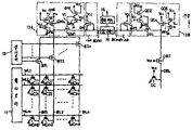
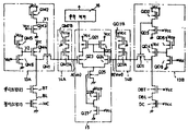
제1도는 종래의 반도체 기억장치로서, 예컨대 부유게이트형 MOSFET를 메모리셀로서 이용하는 EPROM(Erasable and Programmable ROM)을 도시해 놓은 회로도로서, 제1도중 참조부호 MC11, MC12, …, MC1n. …, MCmn은 각각 부유게이트형 MOSFET로 이루어진 메모리셀이고, DC는 부유게이트형 MOSFET로 이루어진 더미셀이며, WL1, WL2, …, WLm은 각각 워드선(행선), BL1, BL2, …, BLn은 각각 비트선(열선), DBL은 더미비트선, 11은 행디코더, 12는 열디코더, BT1, BT2…, BTn은 각각 열선택용 얼게이트 MOSFET, DBT는 상기 열게이트 MOSFET(BT1, BT2, …, BTn)와 등가이면서 게이트에 전원전압(Vcc)이 공급되어 항상 도통상태로 되는 MOSFET, 13A는 N챈널 MOSFET(QM1∼QM6)로 이루어진 제1바이어스전위 설정회로, 14A는 P챈널 MOSFET(QM7)로 이루어진 제1부하회로, 13B는 N챈널 MOSFET(QD1∼QD6)로 이루어진 제2바이어스전위 설정회로, 14B는 P챈널 MOSFET(QD7)로 이루어진 제2부하회로, 15는 센스증폭기, 16은 출력버퍼이다. 또한, 특별히 챈널이 지정되어 있지 않은 MOSFET는 모두 N챈널 MOSFET이다.1 is a circuit diagram showing an EPROM (Erasable and Programmable ROM) using a floating gate MOSFET as a memory cell, as a conventional semiconductor memory device, and the reference numerals MC11, MC12,. , MC1n. … , MCmn are each memory cell composed of floating gate MOSFET, DC is a dummy cell composed of floating gate MOSFET, WL1, WL2,. And WLm are word lines (mapping lines), BL1, BL2,... Where BLn is a bit line (column line), DBL is a dummy bit line, 11 is a row decoder, 12 is a column decoder, BT1, BT2... , BTn is a heat selectable gate MOSFET, DBT is equivalent to the column gate MOSFETs (BT1, BT2, ..., BTn), and the MOSFET is always in a state where the power supply voltage (Vcc) is supplied to the gate, and 13A is an N channel. A first bias potential setting circuit consisting of MOSFETs QM1 to QM6, 14A is a first load circuit consisting of P channel MOSFET QM7, 13B is a second bias potential setting circuit consisting of N channel MOSFETs QD1 to QD6, 14B Is a second load circuit consisting of a P channel MOSFET (QD7), 15 is a sense amplifier, and 16 is an output buffer. In addition, all MOSFETs with no channel specifically designated are N-channel MOSFETs.
그리고, 상기 더미셀(DC)로는 메모리셀[MC ; 메모리셀(MC11∼MCmn)중 임의의 1개를 칭함]과 동일한 MOSFET가 이용되고, 더미비트선(DBL)으로도 비트선[BL ; 비트선(BL1∼BLn)중 임의의 1개를 침함]과 동일한 것이 이용된다.The dummy cell DC may include a memory cell MC; The same MOSFET as that used for any one of the memory cells MC11 to MCmn is used, and the bit line BL is also used as the dummy bit line DBL. Same as any one of the bit lines BL1 to BLn] is used.
상기 제1바이어스전위 설정회로(13A)의 MOSFET(QM1)의 게이트에는 전원전압(Vcc)보다 낮은 전위로 설정되면서 MOSFET(QM2, QM3)로 구성된 정전위 발생회로의 출력노드전위(V1)가 공급되고, MOSFET(QM4)의 게이트에는 상기 노드전위(V1)보다도 낮은 전위로 설정되면서 MOSFET(QM5, QM6)로 구성된 정전위 발생회로의 출력노드전위(V2)가 공급되는데, 여기서 상기 노드전위(V2)의 값은 메모리셀(MC)로 소정 전류가 흐를 때의 비트선(BL)의 전위에 기판바이어스효과에 의한 상승분을 더한 값,즉 N챈널 MOSFET의 임계전압을 더한 값으로 설정된다. 즉, MOSFET(QM4)는 비트선(BL)이 초기상태인 OV로부터 충전될 때에 비트선(BL)을 빠르게 충전시키기 위해 설치된 초기충전용 MOSFET로, 이 MOSFET(QM4)로 비트선전위가 메모리셀(MC)로 소정 전류가 흐를 때의 비트선전위 이상으로 되면 비도통상태로 된다.The output node potential V1 of the potential generating circuit composed of the MOSFETs QM2 and QM3 is supplied to the gate of the MOSFET QM1 of the first bias
이와 같이 구성된 EPROM에서는 더미셀(DC)의 데이터를 기초로 제2부하회로(14B)에서 생성되는 노드(B)의 기준전위(Vref)와, 행디코더(11) 및 열디코더(12)의 출력에 따라 선택된 메모리셀(MC)로부터 독출된 데이터를 기초로 제1부하회로(14A)에서 생성된 노드(A)의 전위(Vin)를 센스증폭기(15)로 비교함으로써 선택된 메모리셀(MC)에 기록되어 있는 데이터를 검출하고, 이 센스증폭기(15)로부터 출력버퍼(16)를 통해 출력시키게 된다.In the EPROM configured as described above, the reference potential Vref of the node B generated in the second load circuit 14B, the output of the
이와 같은 EPROM의 각 메모리셀(MC)에서는 부유게이트에 전자를 선택적으로 주입함으로써 데이터의 프로그램이 행해지게 되는데, 부유게이트에 전자를 주입하는 경우에는 행디코더(11) 및 열디코더(12)에 의해 선택된 비트선(BL) 및 워드선(WL)에 통상의 전원전압(Vcc), 예컨대 5V 보다도 충분히 높은 전압, 예컨대 12.5V∼21V의 전압을 인가함으로써 행해지게 된다.In each memory cell MC of the EPROM, data is programmed by selectively injecting electrons into the floating gate. When electrons are injected into the floating gate, the
즉, 상기한 고전압이 인가되면, 선택된 비트선 및 워드선의 교점에 위치하는 메모리셀의 드레인근방의 챈널영역에서 충격이온화(Impact Ionization)가 발생하게 되고, 이것에 의해 발생된 전자 및 정공쌍중 전자가 메모리셀의 부유게이트로 주입되게 된다. 그리고, 전자가 주입된 메모리셀의 임계전압은 전자가 주입되지 않는 메모리셀의 임계전압보다 높은 값으로 되므로, 부유게이트에 전자가 주입된 메모리셀은 그 제어게이트, 즉 워드선에 "1"레벨의 신호[전원전압(Vcc)]가 공급되어도 오프상태를 유지하게 되고, 이때 전자가 주입되어 있지 않은 메모리셀은 온상태로 된다.That is, when the above high voltage is applied, impact ionization occurs in the channel region near the drain of the memory cell located at the intersection of the selected bit line and word line, and electrons and hole pair electrons generated by this are generated. Is injected into the floating gate of the memory cell. Since the threshold voltage of the memory cell into which electrons are injected becomes higher than the threshold voltage of the memory cell into which electrons are not injected, the memory cell into which the electrons are injected into the floating gate has a "1" level at its control gate, that is, the word line. Is maintained even when the signal (power supply voltage Vcc) is supplied, the memory cell in which no electrons are injected is turned on.
한편, 더미셀(DC)에는 전자가 주입되지 않기 때문에 전자가 주입되어 있지 않은 메모리셀과 등가로 되므로, 이 상태에서는 전위(Vref), (Vin)사이에 전위차가 생기지 않게 된다. 따라서, 전위차가 생기도록 하기 위해 제2부하회로(14B)내의 MOSFET(QD7)의 챈널폭(WD7)을 제1부하회로(14A)내의 MOSFET(QM7)의 챈널폭(WM7) 보다도 크게 해서 MOSFET(QD7)의 전류공급능력이 MOSFET(QM7)보다 커지도록 설정하게 된다. 즉, MOSFET(QD7)의 도통저항을 MOSFET(QM7)의 도통저항보다 작게 설정하게 된다.On the other hand, since electrons are not injected into the dummy cell DC, they are equivalent to the memory cells in which electrons are not injected. In this state, a potential difference does not occur between the potentials Vref and Vin. Therefore, in order to generate the potential difference, the channel width WD7 of the MOSFET QD7 in the second load circuit 14B is made larger than the channel width WM7 of the MOSFET QM7 in the
구체적으로는 MOSFET(QD7)의 도통저항은 기준전위(Vref)가 전자가 주입된 메모리셀이 선택된 경우의 Vin전위와 전자가 주입되지 않은 메모리셀이 선택된 경우의 Vin전위와의 중간전위로 되도록 설정되어 있다. 따라서, 전자가 주입되지 않은 메모리셀이 선택된 경우에도 전위(Vref)와 전위(Vin)사이에 소정의 전위차가 발생하게 된다. 또한, 전자가 주입된 메모리셀이 선택된 경우, 전위(Vin)는 전원전압(Vcc)에서 부하용 MOSFET(QM7)의 임계전압 만큼을 뺀 전위로 설정된다. 또, 이하에는 전자가 주입된 메모리셀, 즉 임계전압이 높은 메모리셀을 "0"기억메모리셀이라 하고, 전자가 주입되지 않은 메모리셀, 즉 임계전압이 낮은 메모니셀을 "1"기억메모리셀로 해서 설명한다.Specifically, the conduction resistance of the MOSFET QD7 is set so that the reference potential Vref is an intermediate potential between the Vin potential when the memory cell into which electrons are injected and the Vin potential when the memory cell to which electrons are not injected is selected. It is. Therefore, even when a memory cell in which electrons are not injected is selected, a predetermined potential difference is generated between the potential Vref and the potential Vin. In addition, when a memory cell into which electrons are injected is selected, the potential Vin is set to a potential obtained by subtracting the power supply voltage Vcc by the threshold voltage of the load MOSFET QM7. In the following description, a memory cell into which electrons are injected, that is, a memory cell having a high threshold voltage, is referred to as a " 0 " memory cell. It explains as follows.
상기와 같은 EPROM에서는 센스증폭기(15)에서 독출된 데이터를 출력버퍼(16)로 수신하고, 이 출력버퍼(16)로부터 외부로 데이터를 출력하게 된다.In the above EPROM, the data read by the
상기 출력버퍼(16)는 데이터출력시에 외부의 큰 부하용량을 충·방전시키게 되므로, 이 출력버퍼(16)로부터 데이터가 출력될 때에는 전원에 노이즈가 발생하여 이 노이즈에 의해 전원전압(Vcc)의 값이 변동하게 된다. 그런데, 상기와 같이 제2부하회로(14B)의 MOSFET(QD7)와 제1부하회로(14A)의 MOSFET(QM7)의 전류공급능력이 다르게 되면 이러한 전원전압의 변동에 대한 응답에 차이가 생겨서 전위(Vin)와 전위 (Vref)의 대소관계가 역전될 수도 있게 되므로, 이것에 의해 센스증폭기(15)로부터 잘못된 데이터가 출력될 우려가 있게 된다. 따라서, 이와 같은 센스증폭기의 오동작을 초래할 수 있는 출력버퍼의 구동을 가능한한 피하는 것이 필요하다.Since the
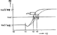
그런데, 제1도에 도시된 EPROM에서는 워드선(WL)을 절환하여 "1"기억메모리셀 다음에 다른 워드선의 "1"기억메모리셀의 데이터를 연속해서 독출하는 경우, 비선택상태로 되는 메모리셀은 바로 오프되지만, 새롭게 선택된 메모리셀은 선택된 초기의 단계에서는 충분하게 온되지 않기 때문에 일시적으로 선택된 비트선의 전위가 상승하게 된다. 즉, 상기와 같은 부유게이트구조의 메모리셀의 임계전압은 2V정도이므로, 워드선의 절환시에 메모리셀은 한순간 오프상태로 되고, 이 때문에 비트선(BL)에서는 워드선의 절환시에 충전작용이 일어나서 제2도에 도시된 노드(A)의 전위(Vin)가 일시적으로 상승하게 된다.However, in the EPROM shown in FIG. 1, when the word line WL is switched to read out the data of the "1" memory memory cell of another word line consecutively after the "1" memory memory cell, it becomes in an unselected state. The memory cell is turned off immediately, but since the newly selected memory cell is not sufficiently turned on in the selected initial stage, the potential of the temporarily selected bit line rises. That is, since the threshold voltage of the memory cell of the floating gate structure as described above is about 2V, the memory cell is turned off for a moment when the word line is switched. Therefore, in the bit line BL, a charging action occurs when the word line is switched. The potential Vin of the node A shown in FIG. 2 temporarily rises.
그런데, 이와 같이 노드(A)의 전위(Vin)가 일시적으로 상승하는데 반해, 더미셀(DC)은 전원전압(Vcc)에 의해 항상 온상태로 되도록 설정되어 있으므로 제2도에 도시된 바와 같이 기준전위(Vref)는 항상 일정하게 된다. 따라서, 제2도에 도시된 바와 같이 전위(Vin)가 기준전위(Vref) 보다 커지게 됨으로써 센스증폭기(15)는 일시적으로 다른 논리레벨의 데이터를 출력하게 되고, 이로 인해 출력버퍼(16)로부터의 출력데이터는 짧은 기간에 "1"레벨-"0"레벨-"1"레벨로 변화하게 된다.However, while the potential Vin of the node A temporarily rises as described above, the dummy cell DC is set to be always turned on by the power supply voltage Vcc, and thus, as shown in FIG. The potential Vref is always constant. Therefore, as shown in FIG. 2, the potential Vin becomes larger than the reference potential Vref, so that the
그리고 이와 같은 출력데이터의 변화는 상기와 같은 전원노이즈의 발생원인으로 되고, 더욱이 출력버퍼(16)의 출력데이터가 "0"레벨로부터 "1"레벨로 변화할 때는 출력버퍼(16)에서 출력용량이 접지전극으로 방전되는 도중에 데이터가 절환되어 그 출력용량이 다시 전원(Vcc)에 의해 충전되는 상태로 되기 때문에 출력버퍼트랜지스터로 흐르는 전류가 단시간에 크게 변화된다. 이 때문에 배선에 존재하는 인덕턴스성분에 의해 접지전압이 크게 변동하여 EPROM내부의 회로가 오동작할 우려가 있게 된다.This change in output data causes the occurrence of power supply noise as described above. Furthermore, when the output data of the
이와 같은 접지전압의 변동에 의한 오동작을 방지하기 위해 종래에는 제3도에 도시된 바와 같은 구성의 EPROM이 고려되었다.In order to prevent a malfunction due to such a change in ground voltage, an EPROM having a configuration as shown in FIG. 3 is conventionally considered.
제3도에 도시된 EPROM은 워드선(WL1∼WLm)에 대응해서 더미셀(DC1∼DCm)이 설치되고, 이 더미셀(DC1∼DCm)의 드레인이 더미비트선(DBL)에 공통접속됨과 더불어 그 더미셀(DC1∼DCm)의 제어게이트가 워드선(WL1∼WLm)에 각각 접속된 구성으로 되어 있다.In the EPROM shown in FIG. 3, dummy cells DC1 to DCm are provided corresponding to the word lines WL1 to WLm, and drains of the dummy cells DC1 to DCm are commonly connected to the dummy bit line DBL. In addition, the control gates of the dummy cells DC1 to DCm are connected to the word lines WL1 to WLm, respectively.
이와 같은 구성으로 하게 되면, 각 더미셀(DC1∼DCm)도 워드선(WL1∼WLm)의 신호에 따라 제어되므로, 워드선(WL1∼WLm)을 절환해서 "1"기억메모리셀의 다음에 다른 워드선의 "1"기억메모리셀의 데이터를 연속해서 독출하는 경우에, 더미비트선(DBL)도 비트선(BL)과 마찬가지로 워드선절환시에 부하회로(14B)에 의한 충전작용을 받게 된다. 따라서, 제4도에 파형도로서 도시된 바와 같이 기준전위(Vref)도 전위(Vin ; "1"레벨)의 상승과 마찬가지로 상승하게 된다. 즉, 이 경우에는 전위(Vin)는 기준전위(Vref)보다 커지지 않게 되고, 출력버퍼(16)로부터의 출력데이터도 변환되지 않게 되며, 접지전압의 변동도 발생되지 않게 된다.According to this configuration, the dummy cells DC1 to DCm are also controlled in accordance with the signals of the word lines WL1 to WLm, so that the word lines WL1 to WLm are switched to be different from each other after the " 1 " memory memory cell. In the case where data of the "1" memory memory cell of the word line is read out continuously, the dummy bit line DBL is subjected to the charging operation by the load circuit 14B at the time of word line switching, similarly to the bit line BL. . Thus, as shown as a waveform diagram in FIG. 4, the reference potential Vref also rises in the same manner as the potential Vin rises. That is, in this case, the potential Vin does not become larger than the reference potential Vref, the output data from the
그러나, 전위(Vin), (Vref)의 상승은 워드선 절환시의 충전작용에 의해 생기기 때문에 부하회로(14A, 14B)내의 MOSFET(QM7, QD7)는 그 전류공급능력차에 의해 상승정도가 다르게 된다. 즉, 상기와 같이 MOSFET(QD7)쪽이 전류공급능력이 크게 설정되어 있기 때문에 제4도에 도시된 바와 같이 전위(Vin ; "1"레벨)에 비해 전위(Vref)는 상당히 높은 레벨까지 상승하게 된다. 이 때문에, 워드선을 절환해서 "1"기억메모리셀로부터 "0"기억메모리셀의 데이터를 독출하는 경우의 독출시간은 제5도에 파형도로 도시된 바와 같이 전위(Vref)가 항상 일정한 때에 비해 T1에 해당되는 시간만큼 지연되게 된다.However, since the rise of the potentials Vin and Vref is caused by the charging action at the time of word line switching, the MOSFETs QM7 and QD7 in the
이와 같이 종래의 반도체 기억장치에서는 선택된 워드선이 절환되는 과도시간에 입력전위가 변동하게 됨으로써 전원에 노이즈가 발생되어 오동작이 유발된다는 결점이 있었다. 또한, 이와 같은 결점을 해결하도록된 종래의 반도체 기억장치에서는 입력전위의 변동에 비해 기준전위의 변동이 커지기 때문에 선택된 워드선이 절환되는 순간에 데이터독출속도가 지연된다고 하는 결점이 있었다.As described above, in the conventional semiconductor memory device, there is a drawback that noise is generated in the power supply due to a change in the input potential at the transient time when the selected word line is switched. In addition, the conventional semiconductor memory device designed to solve such a drawback has a drawback that the data read speed is delayed at the moment the selected word line is switched because the variation of the reference potential is larger than that of the input potential.
그런데, 상기 종래의 반도체 기억장치에 있어서, 워드선 및 비트선이 절환되어 임계전압이 높은 메모리셀(MC)이 선택된 경우, 선택된 비트선(BL)의 제1바이어스전위 설정회로(13A)내의 N채널 MOS트랜지스터(QM4) 및 제1부하회로(14A)의 P챈널 MOS트랜지스터(QM7)를 통해서 흐르는 전류에 의해 충전되게 되는데, 이때 트랜지스터(QM4)의 도통저항은 부하회로(14A)내의 트랜지스터(QM7)보다도 작게 설정되므로 비트선(BL)은 트랜지스터(QM4)에 의해 급속히 충전되게 된다. 그리고, 비트선(BL) 전위가 메모리셀(MC)에 소정 전류가 흐를 때의 비트선전위와 동일하게 될 때까지 충전되게 되면, 그 트랜지스터(QM4)는 비도통상태로 되도록 직류바이어스전위(V2)가 설정되게 되고, 트랜지스터(QM4)가 비도통상태로 된 후에도 비트선(BL)은 트랜지스터(QM7) 및 트랜지스터(QM1)를 통해서 계속 충전되게 된다.By the way, in the conventional semiconductor memory device, when the word line and the bit line are switched so that the memory cell MC having a high threshold voltage is selected, N in the first bias
그리고, 비트선전위가 상승하여 비트선전위가 트랜지스터(QM1)의 게이트에 공급되는 직류바이어스전압(V1) 보다도 그 N챈널 MOS트랜지스터(QM1)의 기판바이어스효과를 고려한 임계전압 만큼 낮은 전위로 되면, 그 트랜지스터(QM1)가 비도통상태로 되게 된다. 그 결과 노드A의 전위(Vin)은 전원전압(Vcc)보다도 P챈널 MOS트랜지스터(QM7)의 임계전압분 만큼 낮은 소정의 하이레벨로 된다.When the bit line potential rises and the bit line potential becomes lower than the DC bias voltage V1 supplied to the gate of the transistor QM1 to a potential lower than the threshold voltage considering the substrate bias effect of the N-channel MOS transistor QM1, The transistor QM1 is brought into a non-conductive state. As a result, the potential Vin of the node A is at a predetermined high level lower than the threshold voltage of the P-channel MOS transistor QM7 than the power supply voltage Vcc.
이와 반대로, 임계전압이 낮은 메모리셀(MC)이 선택되어 그 메모리셀(MC)로 소정의 전류가 흐르게 될 때, 노드A의 전위(Vin)는 트랜지스터(QM7)의 도통저항에 의해 설정되는 소정의 로우레벨로 된다.On the contrary, when the memory cell MC having a low threshold voltage is selected and a predetermined current flows into the memory cell MC, the potential Vin of the node A is set by the conduction resistance of the transistor QM7. It becomes low level of.
한편, 노드B의 전위(Vref)는 상기 노드 A의 전위(Vin)의 진폭의 중간전위로 설정되므로, 임계전압이 낮은 메모리셀이 선택된 경우에는 노드A의 전위(Vin)가 노드 B의 전위(Vref)보다도 낮게 됨과 더불어 센스 증폭기(15)로부터는 논리 "1"의 신호가 출력되고, 반대로 임계전압이 높은 메모리셀이 선택된 경우에는 노드A의 전위(Vin)가 노드B의 전위(Vref)보다도 높게 되므로 센스증폭기(15)로부터는 논리 "0"의 신호가 출 력 된다.On the other hand, since the potential Vref of the node B is set to the intermediate potential of the amplitude of the potential Vin of the node A, when the memory cell having a low threshold voltage is selected, the potential Vin of the node A becomes the potential B of the node B ( The signal of logic "1" is output from the
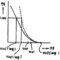
제6도에 상기한 종래의 반도체 기억장치에서의 제1부하회로(14A)의 전압·전류특성을 실선으로 도시해 놓았는바, 제6도에서 횡축은 노드A의 전위(Vin)를, 종축은 그 부하회로(14A)에 흐르는 부하전류를 각각 나타낸다. 그리고, 임계전압이 낮은 메모리셀이 선택되어, Icell의 메모리셀전류(I)가 흐른 때의 노드A의 전위를 Vin("1"레벨), 임계전압이 높은 메모리셀이 선택된 때의 노드 A의 전위를 Vin("0"레벨), 노드 B의 전위를 Vref로 표시했다.In FIG. 6, the voltage and current characteristics of the
그런데, 제1도에 도시된 바와 같은 구성으로 된 불휘발성 반도체 기억장치의 데이터 독출속도는 잘 알려진 바와 같이 워드선의 선택에 필요한 시간과 비트선에 접속되어 있는 접합용량의 충·방전에 필요한 시간이 큰 부분을 차지하고 있는데, 워드선에 있어서의 신호지역시간은 워드선을 구성하는 배선재료의 저항값에 크게 의존하기 때문에 최근에는 종래에 사용되고 있던 다결정실리콘재료 대신에, 보다 저항값이 작은 텅스 텐 실리사이드등의 폴리사이드를 사용하고 있다. 그 결과 데이터의 독출속도는 비트선에 접속되어있는 접합 용량의 충·방전속도에 크게 의존하게 된다. 특히, 비트선이 절환되어 임계전압이 높은 메모리셀이 선택된 경우에는 새롭게 선택된 비트선은 OV로부터 충전되기 때문에 독출속도가 제일 많이 지연되게 된다. 따라서, 고속동작을 실현하기 위해서는 그 경우, 즉 "0"레벨베이터를 독출하는 경우의 독출동작을 바르게 할 필요가 있다.However, as is well known, the data read speed of the nonvolatile semiconductor memory device having the configuration shown in FIG. 1 is a time required for selecting a word line and a time required for charging and discharging a junction capacitance connected to a bit line. It occupies a large part, but since the signal local time of the word line is largely dependent on the resistance value of the wiring material constituting the word line, tungsten silicide having a smaller resistance value instead of the polycrystalline silicon material which has been used in recent years. Polysides, such as these, are used. As a result, the reading speed of the data largely depends on the charging / discharging speed of the junction capacitance connected to the bit line. In particular, when a memory cell having a high threshold voltage is selected because the bit lines are switched, the read speed is most delayed because the newly selected bit line is charged from OV. Therefore, in order to realize the high-speed operation, it is necessary to correct the read operation in that case, that is, in the case of reading the "0" level baiter.
종래에는 노드A의 전위가 Vin("1"레벨) 이하일 때에는 초기충전용 트랜지스터 (QM4)를 통해서 비트선(BL)을 고속으로 충전하도록 되어 있다.Conventionally, when the potential of the node A is equal to or lower than Vin ("1" level), the bit line BL is charged at a high speed through the initial charge transistor QM4.
그러나, 비트선(BL)의 전위가 Vin("1"레벨)이상으로 되면 트랜지스터(QM4)가 비도통상태로 되어 비트선(BL)을 충전시키는 트랜지스터는 부하회로(14A)내의 트랜지스터(QM7)만으로 된다. 그런데, 이 P챈널 트랜지스터(QM7)는 게이트가 그 드레인에 접속되어 있기 때문에 노드A의 전위(Vin)가 상승하게 되면 도통저항이 급격히 높아지면서 충전전류는 급격히 감소하게 된다. 이 때문에 노드A의 전위가 Vin("1"레벨)으로 부터 Vin("0"레벨)까지 상승하기에는 많은 시간이 필요로 되기 때문에 독출속도가 지연되게 된다.However, when the potential of the bit line BL is above Vin (" 1 " level), the transistor QM4 is in a non-conductive state, and the transistor for charging the bit line BL is the transistor QM7 in the
한편, 트랜지스터(QM7)의 챈널폭을 크게 해서 도통저항이 작아지도록 하게 되면, 노드A의 전위가 전위[Vin("1"레벨)]로부터 전위[Vin("0"레벨)]로 될 때까지의 시간을 단축할 수 있지만, 이렇게 트랜지스터(QM7)의 도통저항을 작게 설명하게 되면 전원노이즈에 대한 마진이 저하되는 것과 같은 문제가 생기게 된다.On the other hand, when the channel width of the transistor QM7 is increased so that the conduction resistance becomes smaller, the potential of the node A becomes from the potential Vin ("1" level) to the potential [Vin ("0" level)]. Although the time can be shortened, if the conduction resistance of the transistor QM7 is described as small, there is a problem that the margin for power supply noise is reduced.
제6도에 점선으로 도시되어 있는 특성은 트랜지스터(QM7)의 도통저항을 1/2로 설정한 경우의 특성을 나타낸 것으로, 트랜지스터(WM7)의 도통저항을 1/2로 설정하게 되면, "1"레벨데이터의 기억셀, 즉 임계 전압이 낮은 셀이 선택된 때의 노드 A의 전위 (Vin)는 Vin("1"레벨)'로 된다.6 shows the characteristic when the conduction resistance of the transistor QM7 is set to 1/2. When the conduction resistance of the transistor WM7 is set to 1/2, " 1 " "The potential Vin of the node A when the memory cell of the level data, that is, the cell having a low threshold voltage is selected, becomes Vin (" 1 "level)".
통상, 노드B의 전위(Vref)는 "1"레벨데이터의 기억셀이 선택된 때의 노드A의 전위[Vin("1"레벨)]와, "0"레벨데이터의 기억셀, 즉 임계전압이 높은 셀이 선택된 때의 노드A의 전위[Vin("0"레벨)]의 정확히 중간전위로 되도록 설정된다. 따라서, 트랜지스터(QM7)의 도통저항을 1/2로 설정하는 경우의 노드B의 전위는[Vin("0"레벨)-Vin("1"레벨)]/2인 기준 전압으로 되도록 제2부하회로(14B)내의 P챈널 MOS트랜지스터(QD7)의 도통저항을 설정해야 하는 바, 그 결과 "1"또는 "0"레벨 데이타의 기억셀이 선택된 때 노드B의 전위와 노드A의 전위사이의 차는 [Vin("1"레벨)-Vin("1"레벨)]/2만큼 작아지게 된다.Normally, the potential Vref of the node B is equal to the potential [Vin ("1" level)) of the node A when the storage cell of "1" level data is selected and the storage cell of the "0" level data, that is, the threshold voltage. It is set to be exactly intermediate potential of the potential Vin ("0" level) of node A when the high cell is selected. Therefore, when the conduction resistance of the transistor QM7 is set to 1/2, the second load is such that the potential of the node B becomes a reference voltage of [Vin ("0" level)-Vin ("1" level)] / 2). The conduction resistance of the P-channel MOS transistor QD7 in the circuit 14B must be set. As a result, the difference between the potential of the node B and the potential of the node A when the memory cell of "1" or "0" level data is selected is selected. [Vin ("1" level) -Vin ("1" level)] / 2 becomes smaller.
일반적으로 출력버퍼회로로부터 데이터가 출력될 때에는 상기한 바와 같이 전압이 크게 변동되기 때문에 노드A와 노드B의 전위도 변동하게 된다. 그리고 제1 및 제2부하회로(14A, 14B)에서는 도통저항의 값에 차이가 있기 때문에 노드A 및 노드B의 전위변화정도가 다르게 되는데, 이때 양 노드간의 전위차가 작아지게 되면 접지전압이 변동될 때에 센스증폭기(15)가 데이터를 잘못 검출할 우려가 있게 된다.In general, when data is output from the output buffer circuit, the voltage of the node A and the node B also varies because the voltage varies greatly as described above. In the first and
이와 같이, 종래의 반도체 기억장치에 있어서는 부하회로의 도통저항의 값을 작게 설정해서 독출속도의 고속화를 도모하게 되면 전원노이즈에 의해 오동작이 쉽게 일어나게 된다는 문제가 있게 된다.As described above, in the conventional semiconductor memory device, if the conduction resistance of the load circuit is set small and the read speed is increased, there is a problem that malfunction occurs easily due to power supply noise.
[발명의 목적][Purpose of invention]
본 발명은 상기한 점을 감안해서 발명된 것으로, 그 제1목적은 워드선의 선택이 절환되는 과도기간에도 전원에 노이즈가 발생되지 않고, 또 데이터독출속도의 향상을 도모할 수 있도록 된 반도체 기억장치를 제공함에 있고, 그 제2목적은 노이즈에 의한 전원전압의 변동에 대해서 높은 동작마진을 갖추고, 동작속도의 고속화를 용이하게 도모할 수 있도록 된 반도체기억장치를 제공함에 있다.The present invention has been made in view of the above-mentioned point, and its first object is to provide a semiconductor memory device in which no noise is generated in the power supply even during a transient period in which the word line selection is switched, and the data reading speed can be improved. The second object of the present invention is to provide a semiconductor memory device which has a high operating margin against fluctuations in power supply voltage due to noise and can easily increase the operating speed.
[발명의 구성 및 작용][Configuration and Function of Invention]
제1목적을 실현하기 위한 본 발명의 제1실시예에 따른 반도체 기억장치는, 워드선(WL1∼WLm)과, 이 워드선(WL1∼WLm)에 의해 선택되는 메모리셀(MC11∼MCmn), 이 메모리셀(MC11∼MCmn)로부터의 데이터가 인가되는 비트선(BL1∼BLn), 이 비트선(BL1∼BLn)에 접속되는 제1부하회로(14A), 상기 워드선(WL1∼WLm)에 의해 선택되는 제1더미셀(DC1∼DCm), 이 제1더미셀(DC1∼DCm)이 접속되는 더미비트선(DBL), 이 더미비트선(DBL)에 접속되는 제2부하회로(14B) 및, 상기 비트선(BL1∼BLm)과 상기 더미비트선(DBL)의 전위차를 기초로 상기 메모리셀(MC11∼MCmn)의 기억데이터를 검출하는 센스증폭기(15)를 구비하여 이루어진 반도체 기억장치에 있어서, 상기 더미비트선(DBL)에 접속되면서 게이트에 소정 전위가 공급되는 제2더미셀(DCm+1)을 더 구비하여 구성된 것을 특징한다.The semiconductor memory device according to the first embodiment of the present invention for realizing the first purpose includes word lines WL1 to WLm, memory cells MC11 to MCmn selected by the word lines WL1 to WLm, To the bit lines BL1 to BLn to which data from the memory cells MC11 to MCmn is applied, to the
또한, 상기 제1목적을 실현하기 위한 본 발명의 제2실시예에 따른 반도체 기억장치는, 워드선(WL1∼WLm)과, 이 워드선(WL1-WLm)에 의해 선택되는 메모리셀(MC11∼MCmn), 이 메모리셀(MC11∼MCmn)로부터의 데이터가 인가되는 비트선(BL1∼BLn)에 접속되는 제1부하회로(14A), 상기 워드선(WL1∼WLm)에 의해 선택되는 제1더미셀(DC1∼DCm), 이 제1더미셀(DC1∼DCm)이 접속되는 더미비트선(DBL), 이 더미비트선(DBL)에 접속되는 제2부하회로(14B) 및, 상기 비트선(BL1∼BLm)과 상기 더미비트선(DBL)의 전위차를 기초로 상기 메모리셀(MC11∼MCmn)의 기억데이터를 검출하는 센스증폭기(15)를 구비하여 이루어진 반도체 기억장치에 있어서, 어드레스 입력의 변화를 검출해서 펄스신호를 발생시키는 펄스신호 발생회로(18)와, 상기 더미비트선(DBL)에 접속되면서 상기 펄스신호에 의해 도통제어되는 제2더미셀(DCm+1)을 더 구비하여 구성된 것을 특징으로 한다.Further, the semiconductor memory device according to the second embodiment of the present invention for realizing the first purpose includes the memory lines MC11 to WLm selected from the word lines WL1 to WLm and the word lines WL1-WLm. MCmn, a
그리고, 상기 제1목적을 실현하기 위한 본 발명의 제3실시예에 따른 반도체 기억장치는, 워드선(WL1∼WLm)과 이 워드선(WL1∼WLm)에 의해 선택되는 메모리셀(MC11∼MCmn), 이 메모리셀(MC11∼MCmn)로부터의 데이터가 인가되는 비트선(BL1∼BLn)이, 이 비트선(BL1∼BLn)에 접속되는 제1부하회로(14A), 상기 워드선(WL1∼WLm)에 의해 선택되는 제1더미셀(DC1∼DCm), 제1더미셀(DC1∼DCm)이 접속되는 더미비트선(DBL) 및 상기 비트선(BL1∼BLm)과 상기 더미비트선(DBL)의 전위차를 기초로 상기 메모리셀(MC11∼MCmn)의 기억데이터를 검출하는 센스증폭(15)를 구비하여 이루어진 반도체 기억장치에 있어서, 어드레스 입력의 변화를 검출해서 펄스신호를 발생시키는 펄스신호 발생회로(18)와, 상기 더미비트선(DBL)에 접속되면서 상기 펄스신호에 따라 상기 더미비트선(DBL)에 대한 전류공급능력이 제어되는 제2부하회로(14B)를 더 구비하여 구성된 것을 특징으로 한다.In the semiconductor memory device according to the third embodiment of the present invention for realizing the first purpose, the memory cells MC11 to MCmn selected by the word lines WL1 to WLm and the word lines WL1 to WLm. ), The
상기와 같이 구성된 본 발명에 의하면, 항상 또는 워드선 절환시의 과도시간에 온상태로 제어되는 제2더미셀을 더미비트선에 접속하거나, 또는 워드선 절환시에 더미비트선으로 흐르는 전류량을 변화시킴으로써 워드선 절환시의 기준전위 상승을 억제할 수 있게 된다.According to the present invention configured as described above, the second dummy cell which is always controlled on or at the transient time at the time of word line switching is connected to the dummy bit line, or the amount of current flowing to the dummy bit line at the time of word line switching is changed. This makes it possible to suppress a rise in the reference potential at the time of word line switching.
더욱이, 제2부하회로의 더미비트선에 대한 전류공급능력을 워드선 절환시의 과도기간에 변화시킴으로써 워드선 절환시의 기준전위상승을 억제할 수 있게 된다.Further, by changing the current supply capability of the dummy bit line of the second load circuit in the transient period at the time of word line switching, the reference potential rise at the time of word line switching can be suppressed.
또한, 상기 제2목적을 실현하기 위한 본 발명의 제4실시예에 따른 반도체 기억장치는, 메모리셀(MC)과, 소오스·드레인중 한쪽이 상기 메모리셀(MC)의 드레인에 결합되면서 다른 한쪽이 데이터검출노드(A)에 각각 결합됨과 더불어 그 게이트에 제1직류바이어스 전압(V1)이 공급되는 제1MOS트랜지스터(QM1)와, 소오스·드레인중 한쪽이 상기 메모리셀(MC)의 드레인에 결합되면서 다른 한쪽이 상기 제1전원전위(Vcc)에 결합됨과 더불어 게이트에 상기 제1직류바이어스전압(V1) 보다 낮은 제2직류바이스전압(V2)이 공급되는 제2MOS트랜지스터(QM4) 및 상기 데어이터검출노드(A)에 접속되어 상기 메모리셀(MC)의 기억 데이터를 독출하는 센스증폭기(15)를 구비하여 이루어진 반도체 기억장치에 있어서, 상기 데이터검출노드(A)와 제1전원전위(Vcc) 사이에 삽입되면서 상기 메모리셀(MC)이 도통상태인 때에는 정전류동작을 하는 제1부하수단과, 상기 메모리셀(MC)이 비도통상태인 때에는 상기 데이터검출노드(A)의 전위가 상기 제1전원 전위(Vcc) 보다도 낮아지도록 제어하는 제2부하수단이 직렬접속되고, 상기 제1부하수단의 도통저항값이 상기 메모리셀(MC)이 도통상태인 때의 상기 제2부하수단의 도통저항값보다 크게 되도록 설정된 부하회로(14A)를 더 구비하여 구성된 것을 특징으로 한다.In addition, in the semiconductor memory device according to the fourth embodiment of the present invention for realizing the second purpose, one of the memory cell MC and the source / drain is coupled to the drain of the memory cell MC, and the other. One of the first MOS transistor QM1 and the source and drain coupled to the data detection node A and supplied with the first DC bias voltage V1 to the gate thereof is coupled to the drain of the memory cell MC. The second MOS transistor QM4 and the data coupled to the first power potential Vcc and supplied with a second DC bias voltage V2 lower than the first DC bias voltage V1 to the gate. A semiconductor memory device comprising a
상기와 같이 구성된 본 발명에 따른 반도체 기억장치에 의하면, 메모리셀이 도통되어 소정의 전류가 흐를 때에는 주로 부하회로내의 제1부하수단에 의해 부하회로를 흐르는 전류량이 결정되고, 부하회로에서는 도통저항값은 주로 그 제1부하수단에서의 도통저항에 의해 결정된다.According to the semiconductor memory device according to the present invention configured as described above, when the memory cell is conducted and a predetermined current flows, the amount of current flowing through the load circuit is mainly determined by the first load means in the load circuit. Is mainly determined by the conduction resistance in the first load means.
한편, 메모리셀이 비도통상태인 때에는 데이터검출노드의 전위가 상승하여 그 값이 소정값에 도달 된 때에는 부하회로내의 제2부하수단이 비도통상태로 되므로 데이터 검출노동의 전위는 전원전압보다도 소정값만큼 낮은 값으로 설정되게 된다.On the other hand, when the memory cell is in a non-conducting state, when the potential of the data detection node rises and the value reaches a predetermined value, the second load means in the load circuit becomes the non-conducting state. It will be set as low as.
[실시예]EXAMPLE
이하, 예시도면을 참조해서 본 발명에 따른 1실시예를 상세히 설명한다.Hereinafter, an embodiment according to the present invention will be described in detail with reference to the accompanying drawings.
제7도는 본 발명의 1실시예에 따른 반도체 기억장치로서, 종래와 마찬가지로 부유게이트형 MOSFET를 메모리셀로 이용한 EPROM에 본 발명을 적용한 경우의 전체구성을 도시해 놓은 회로도이다.FIG. 7 is a circuit diagram showing the overall configuration when the present invention is applied to an EPROM using a floating gate type MOSFET as a memory cell as a conventional semiconductor memory device according to one embodiment of the present invention.
제7도에 있어서, 참조부호 MC11, MC12, …MC1n, …, MCmn은 각각 부유게이트형 MOSFET로 이루어진 메모리셀이고, DC1, DC2, …, DCm은 각각 부유 게이트형 MOSFET로 이루어진 더미셀(제1더미셀)이며, DCm+1은 부유게이트형 MOSFET로 이루어진 더미셀(제2더미셀), WL1, WL2, …, WLm은 각각 워드선, BL1, BL2, …, BLn은 각각 비트선, DBL은 더미비트선, 11은 행디코더, 12는 열디코더 BT1, BT2, …, BTn은 각각 열선택용 열게이트 MOSFET, DBT는 열게이트 MOSFET와 등가이면서 게이트에 전원전압(Vcc)이 공급되어 항상 도통상태로 디는 MOSFET, 13A는 N챈널 MOSFET(QM1∼QM6)로 이루어진 제1바이어스전위 설정회로, 14A는 P챈널 MOSFET(QM7)로 이루어진 제1부하회로, 13B는 N챈널 MOSFET(QD1∼QD6)로 이루어진 제2바이어스전위 설정회로, 14B는 P챈널 MOSFET(QD7)로 이루어진 제2부하회로, 15는 센스 증폭기, 16은 출력버퍼이다. 또 본 실시예의 경우에도 특별히 챈널을 지정하지 않은 MOSFET는 모두 N챈널 MOSFET이다.In Fig. 7, reference numerals MC11, MC12,... MC1n,... And MCmn are memory cells each consisting of floating gate MOSFETs, and DC1, DC2,... , DCm is a dummy cell (first dummy cell) consisting of floating gate MOSFETs, and DCm + 1 is a dummy cell (second dummy cell) consisting of floating gate MOSFETs, WL1, WL2,. And WLm are word lines BL1, BL2,... BLn is a bit line, DBL is a dummy bit line, 11 is a row decoder, 12 is a column decoder BT1, BT2,... BTn is the column gate MOSFET for thermal selection, DBT is equivalent to the column gate MOSFET, and the power supply voltage (Vcc) is supplied to the gate so that it always turns on and 13A is composed of N channel MOSFETs (QM1 to QM6). 1 bias potential setting circuit, 14A is a first load circuit composed of P channel MOSFET (QM7), 13B is a second bias potential setting circuit composed of N channel MOSFETs (QD1 to QD6), and 14B is composed of P channel MOSFET (QD7). The second load circuit, 15 is a sense amplifier and 16 is an output buffer. Also in the present embodiment, all the MOSFETs not specifically designated are N-channel MOSFETs.
상기 각 더미셀(DC1, DC2, …, DCm)은 각 드레인이 상기 더미비트선(DBL)에 공통으로 접속되고, 또 각 게이트는 상기 워드선(WL1∼WLm)에 각각 접속되며, 각 소오스는 접지되어 있다. 더욱이, 상기 더미셀(DCm+1)의 드레인은 상기 더미비트선(DBL)에 접속되는데, 그 제어게이트에는 전원전압(Vcc)이 항상 공급되고, 소오스는 접지되어 있다.In each of the dummy cells DC1, DC2, ..., DCm, each drain is connected to the dummy bit line DBL in common, and each gate is connected to the word lines WL1 to WLm, respectively. It is grounded. Further, the drain of the dummy cell DCm + 1 is connected to the dummy bit line DBL. A power supply voltage Vcc is always supplied to the control gate, and the source is grounded.
상기 제1 및 제2바이어스전위 설정회로(13A, 13B)는 각각 종래의 것과 동일한 구성으로 되어 있다. 옐르들어, 제1바이어스전위 설정회로(13A)는 열게이트 MOSFET(BT1∼BTn)의 공통접속점과 노드A의 사이에 MOSFET(QM1)의 소오스·드레인간의 전류통로가 삽입되어 있고, 그 MOSFET(QM1)의 게이트에는 2개의 MOSFET(QM2, QM3)에 의해 형성된 전원전압(Vcc)보다 낮은 직류바이어스전위(V1)가 공급된다. 또, 상기 열게이트 MOSFET(BT1∼BTn)의 공통접속점과, 전원전압(Vcc)사이에는 MOSFET(QM4)의 소오스·드레인간의 전류통로가 삽입되어 있는데, 이 MOSFET(QM4)의 게이트에는 2개의 MOSFET(QM5, QM6)에 의해 형성된 상기 직류바이어스전위(V1)보다도 낮은 값의 직류바이어스전위(V2)가 공급된다.The first and second bias
그리고, 이 직류바이어스전위(V2)의 값은, 임계전압이 낮게 설정되어 있는 메모리셀이 선택되어 그 소오스·드레인전류통로에 소정 전류가 흐르는 때의 비트선전위에 기판바이어스효과를 고려한 N챈널 MOSFET의 임계전압을 더한 값으로 설정된다. 또한 제2바이어스전위 설정회로(13B)는 그 MOSFET(QD1∼QD6)를 제1바이어스전위 설정회로(13A)의 MOSFET(QM1∼QM6)에 대응시킨 것으로, 실질적으로 동일한 구 성으로 되어 있다.The value of the DC bias potential V2 is the value of the N-channel MOSFET that considers the substrate bias effect on the bit line potential when a memory cell having a low threshold voltage is selected and a predetermined current flows through the source / drain current path. The threshold voltage is set to the value. The second bias
또한, 상기 제1바이어스전위 설정회로(13A)내에 설치되어 있는 MOSFET(QM4)는 선택된 비트선(BL)이 초기값인 OV로부터 충전될 때에 그 비트선을 빠르게 충전시킬 목적으로 설치된 충전용 트랜지스터로 이 MOSFET(QM4)는 비트선전위가 메모리셀에 소정 전류가 흐를때의 비트전위 이상으로 되면 오프상태로 되도록 직류바이어스전위(V2)가 설정되어 있다.Further, the MOSFET QM4 provided in the first bias
더욱이 제1 및 제2부하회로(14A, 14B)도 각각 종래와 동일한 구성으로 되어 있다. 즉, 제1부하회로(14A)에서는 노드A와 전원전압(Vcc)의 사이에 P챈널 MOSFET(QM7)의 소오스·드레인간 전류통로가 삽입되어 있고, 그 MOSFET(QM7)의 게이트는 그 드레인측, 즉 노드A에 접속되어 있다.Further, the first and
또, 제2부하회로(14B)는 MOSFET(QD7)를 상기 MOSFET(QM7)에 대응시킨 것으로, 이것도 마찬가지로 구성되어 있다.The second load circuit 14B corresponds to the MOSFET QM7 with the MOSFET QD7, which is similarly configured.
그러나, 더미비트선(DBL)에는 그 게이트에 전원(Vcc)이 항상 공급되어 항상 온상태로 되어 있는 더미셀(DCm+1)이 접속되어 있기 때문에, 그 더미비트선(DBL)은 더미셀(DCm+1)과 선택된 워드선(WL)에 접속된 더미셀[DC ; 더미셀(DC1∼DCm)중 임의의 1개를 칭함]을 통해서 방전된다. 이 때문에 기준전위(Vref)가 입력전위(Vin)의 "1"레벨과 "0"레벨의 정확한 중간전위를 유지하게 됨으로써 제2부하회로(14B)내의 부하용 MOSFET(QD7)의 전류공급능력은 상기 제1도에 도시된 종래의 장치의 MOSFET(QD7)이 전류공급능력보다 약 2배 정도로 설정되게 된다.However, the dummy bit line DBL is connected to the dummy cell DCm + 1 in which the power supply Vcc is always supplied to its gate and is always on, so that the dummy bit line DBL is a dummy cell ( A dummy cell [DC; connected to the DCm + 1) and the selected word line WL; And any one of the dummy cells DC1 to DCm. For this reason, the reference potential Vref maintains the correct intermediate potential between the "1" level and the "0" level of the input potential Vin, so that the current supply capability of the load MOSFET QD7 in the second load circuit 14B is reduced. The MOSFET QD7 of the conventional device shown in FIG. 1 is set to about twice the current supply capability.
이어 상기와 같이 구성된 반도체 기억장치에 있어서, 워드선을 절환하여 서로 다른 워드선에 의해 선택되는 2개의 메모리셀로부터 연속해서 데이터를 독출하는 경우의 동작을 설명한다.Next, in the semiconductor memory device configured as described above, an operation in the case of reading data sequentially from two memory cells selected by different word lines by switching word lines will be described.
워드선의 절환을 행할 때에는 제8a도에 파형도로서 도시되어 있는 바와같이, 비선택상태로 되는 쪽의 워드선(WLi; i=1, 2---, m)의 전위는 "1"레벨로부터 "0"레벨로 저하되고, 선택상태로 되는 쪽의 워드선(WLj; j=1, 2, ---, m)의 전위는 "0"레벨로부터 "1"레벨로 상승하게 된다.When switching word lines, as shown by the waveform diagram in FIG. 8A, the potential of the word line WLi (i = 1, 2 ---, m) in the non-selected state is from the " 1 " level. The potential of the word line WLj (j = 1, 2, ---, m) on the side which is lowered to the "0" level and is in the selected state is raised from the "0" level to the "1" level.
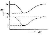
이 워드선의 절환시에 더미셀에 흐르는 전류를 제8도에 도시해 놓았다. 즉, 도면중 전류(x)의 값은 전원(Vcc)이 제어게이트에 공급된 때에 선택된 더미셀(DC)에 흐르는 전류와 동일하다. 본 실시예에서는 더미셀(DC)은 메모리 매트릭스내의 메모리셀과 동일한 구조와 동일한 챈널폭, 동일 챈널길이를 갖는 부유게이트구조의 MOS트랜지스터를 사용하게 되므로, 전원(Vcc)이 제어게이트에 공급될 때 메모리셀에 흐르는 전류는 x와 동일하게 된다. 이 때문에 더미셀(DCm+1)에 흐르는 전류도 x와 동일하게 되고, 워드선이 전환되기 전에 모든 더미셀에 흐르는 전류는 2x로 된다.The current flowing in the dummy cell at the time of switching of the word lines is shown in FIG. That is, the value of the current x in the figure is equal to the current flowing through the selected dummy cell DC when the power supply Vcc is supplied to the control gate. In the present embodiment, since the dummy cell DC uses a MOS transistor having a floating gate structure having the same structure, the same channel width, and the same channel length as that of the memory cells in the memory matrix, the power supply Vcc is supplied to the control gate. At this time, the current flowing in the memory cell becomes equal to x. For this reason, the current flowing in the dummy cell DCm + 1 is also equal to x, and the current flowing in all dummy cells before the word line is switched is 2x.
더미셀(DC)에 흐르는 전류의 최소값을 y로 표시하면, 본 실시예에서는 워드선의 전환시에 모든 더미셀에 흐르는 전류의 최소값은 x+y로 된다.If the minimum value of the current flowing in the dummy cell DC is denoted by y, in this embodiment, the minimum value of the current flowing in all the dummy cells at the time of word line switching becomes x + y.
또, 제8b도중의 일점쇄선은 상기한 제8a도에서 설명한 워드선의 전환시에 상기 제1도에 도시된 종래 장치의 더미셀에 흐르는 전류의 변화를 나타낸 것이다.In addition, the dashed-dotted line in FIG. 8B shows the change in the current flowing through the dummy cell of the conventional apparatus shown in FIG. 1 at the time of switching the word line described in FIG. 8A.
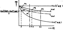
제9도는 돔셀에 흐르는 전류에 대한 기준전위(Vref)의 레벨(실선)을 도시해 놓은 도면이다. 또, 제9도에는 기준 전위(Vref)와 더불어 "1"기억메모리셀의 데이터를 독출할 때에 얻어지는 노드A의 전위[Vin("1" 레벨)] 및 "0"기억메모리셀의 데이터를 독출할 때는 얻어지는 노드A의 전위[Vin("0"레벨)]인 메모리셀에 흐르는 전류에 대한 레벨(실선)과, 제1도에 도시된 종래 반도체 기억장치의 더미셀에 흐르는 전류에 대한 기준전압(Vrdf)의 레벨(일점쇄선)도 병행해서 도시되어 있다.9 is a diagram showing the level (solid line) of the reference potential Vref with respect to the current flowing through the dome cell. 9 also reads the data of the node A obtained at the time of reading the data of the "1" memory memory cell (Vin ("1" level)) and the data of the "0" memory memory cell together with the reference potential Vref. At the time of shipment, the level (solid line) for the current flowing through the memory cell which is the potential [Vin ("0" level)) of the node A obtained, and the reference voltage for the current flowing through the dummy cell of the conventional semiconductor memory device shown in FIG. The level (dotted and dashed line) of (Vrdf) is also shown in parallel.
본 실시예에서는 어느 하나의 워드선이 선택될 경우, 그 선택된 워드선에 더미셀 외에 항상 구동되고 있는 더미셀(DCm+1)이 더미비트선(DBL)에 접속되어 있기 때문에, 2배의 셀전류가 흐른 때에 종래와 동일한 값의 기준전위가 얻어지도록 제2부하회로(14B)내의 MOSFET(QD7)의 전류 공급능력을 설정하게 된다. 즉 제1도에 도시된 종래 장치에서의 기준전위(Vref)는 더미셀에 흐르는 전류값이 2x인 점(P2)에서 [Vin("0"레벨)-Vin("1"레벨)]/2로 되도록 MOSFET(QD7)의 도통저항이 설정된다.In this embodiment, when any word line is selected, since the dummy
이와 같은 전위(Vref)의 변화 특성을 가짐으로서 인해 워드선의 절환시에 더미셀로 흐르는 전류의 값이 가장 작아져서 (전류값 y의 점) 전위[Vin("1"레벨)]가 도면중의 P3점까지 상승될 때, 제1도에 도시된 종래의 반도체 기억장치에서의 기준전위(Vref)는 P4점의 전위까지 상승하게 된다. 이에 대해 본 실시예에 따른 반도체 기억장치의 경우에 기준전위(Vref)는 더미셀로 흐르는 전류가 x+y로 되기 때문에 P5점의 전위까지밖에 상승하지 않게 된다.By having such a change characteristic of the potential Vref, the value of the current flowing to the dummy cell at the time of switching the word line is the smallest (point of current value y) and the potential [Vin ("1" level)) is shown in the figure. When raised to the point P3, the reference potential Vref in the conventional semiconductor memory device shown in FIG. 1 rises to the potential of the point P4. On the other hand, in the case of the semiconductor memory device according to the present embodiment, the reference potential Vref only rises to the potential at P5 because the current flowing through the dummy cell becomes x + y.
제10도는 상기 실시예에 있어서, 워드선을 절환해서 "1"기억, 즉 임계전이 낮은 메모리셀의 다음에 다른 워드선 "1"기억메모리셀의 데이터를 연속해서 독출하는 경우의 기준전위(Vref)와 전위[Vin("1"레벨)]의 변화를 도시한 파형도로서, 상기한 바와 같이 워드선의 절환시 더미셀로 흐르는 전류가 가장 작아진 때에는 기준전위(Vref)가 상승하는 레벨은 상기 제4도에 도시된 바와 같이, 제3도에 도시된 종래 반도체 기억장치의 기준전위(Vref)의 상승 정도에 비해 대폭 억제된다.FIG. 10 shows the reference potential in the case of reading the data of another word line " 1 " memory cell consecutively after the " 1 " Vref) and the potential [Vin ("1" level)] is a waveform diagram showing the change. As described above, the level at which the reference potential Vref rises when the current flowing to the dummy cell becomes the smallest when the word line is switched. As shown in FIG. 4, the degree of increase of the reference potential Vref of the conventional semiconductor memory device shown in FIG. 3 is significantly suppressed.
더욱이, 제1도에 도시된 종래 반도체 기억장치에서 알 수 있는 바와 같이 기준전위(Vref)가 전위(Vin)와 비교되지 않기 때문에 출력버퍼동작에 의한 전원노이즈의 발생이 억제되게 된다.Further, as can be seen in the conventional semiconductor memory device shown in FIG. 1, since the reference potential Vref is not compared with the potential Vin, generation of power supply noise due to the output buffer operation is suppressed.
또한, 제11도에 파형도로서 나타낸 바와 같이 워드선을 절환해서 "1"기억메모리셀로 "1"기억메모리셀의 데이터를 독출하는 경우에는 제11도에 점선으로 도시되어 있는 종래의 기준전위 상승에 비해 일점쇄선으로 도시되어 있는 본 실시예에 다른 따른 반도체 기억장치에서의 기준 전위 상승이 작아진 만큼 독출속도가 빨라지기 때문에, T2 만큼 데이터 독출속도의 고속화를 도모할 수 있게 된다.As shown by the waveform diagram in FIG. 11, when the word lines are switched to read data of the "1" memory memory cell into the "1" memory memory cell, the conventional reference shown by the dotted line in FIG. As the reference potential rise in the semiconductor memory device according to the present embodiment shown by the dashed-dotted line is smaller than the potential rise, the read speed is increased, so that the data read rate can be increased by T2.
또, 제7도에 도시된 실시예에서는 더미셀(DCm+1)의 게이트에 전원전압(Vcc)을 공급하는 경우에 대해서 설명했지만, 이는 일정전압이면 전원전압(Vcc)에 한정되지 않고, 그 일정전압의 레벨을 기초로 기준전위를 조정하는 것도 가능하게 된다.In addition, in the embodiment shown in FIG. 7, the case where the power supply voltage Vcc is supplied to the gate of the dummy cell DCm + 1 has been described. However, this is not limited to the power supply voltage Vcc. It is also possible to adjust the reference potential based on the level of the constant voltage.
또한, 본 실시예에서는 워드선에 의해 제어되는 m개의 더미셀(DC1∼DCm)과 더미셀(DCm+1)을 동일한 더미비트선(DBL)으로 접속하는 경우에 대해 설명했지만, 더미셀(DCm+1)에 대해 독립적으로 더미비트선과 열게이트 MOSFET와 등가인 MOSFET 및 부회회로를 각각 설치하고, 양 부하회로의 출력을 센스증폭기(15)의 입력에 접속하여도 동일한 효과를 얻을수 있게 된다.In this embodiment, the case where m dummy cells DC1 to DCm and dummy cells DCm + 1 controlled by a word line are connected to the same dummy bit line DBL has been described. The same effect can be obtained even when the MOSFET and the auxiliary circuit equivalent to the dummy bit line and the column gate MOSFET are independently provided for +1), and the outputs of both load circuits are connected to the inputs of the
제12도는 본 발명의 제2실시예에 따른 반도체 기억장치를 도시해 놓은 회로도로서, 본 실시예에 따른 반도체 기억장치도 제7도에 도시된 반도체 기억장치와 마찬가지로 부유게이트형 MOSFET를 메모리셀로서 이용한 EPROM에 본 발명을 실시한 것이다.FIG. 12 is a circuit diagram showing a semiconductor memory device according to a second embodiment of the present invention. Similarly to the semiconductor memory device shown in FIG. 7, the semiconductor memory device according to the present embodiment uses a floating gate MOSFET as a memory cell. This invention is implemented to the used EPROM.
본 실시예에 따른 반도체 기억장치가 제7도에 도시된 제1실시예에 따른 반도체 기억장치와 다른 점은 상기 더미셀(DCm+1)의 게이트에 항상 공급해던 전원전압(Vcc)을 공급하는 대신에 행어드레스가 공급되는 행어드레스버퍼(17)의 출력을 인가받아, 행어드레스가 변화된 후 워드선이 절환될 때에 소정의 펄스폭을 갖춘 펄스신호를 발생시키는 어드레스천이 검출기(18; 펄스신호 발생회로; 이하, ATD라 칭함)를 설치하고, 이 ATD(18)로부터의 출력펄스신호를 상기 더미셀(DCm+1)의 게이트에 공급하도록되어 있는 점이다.The semiconductor memory device according to the present embodiment differs from the semiconductor memory device according to the first embodiment shown in FIG. 7 in that the power supply voltage Vcc is always supplied to the gate of the dummy
또한, 제12도에 있어서 참조부호 19는 열어드레스가 공급되는 열어드레스버퍼이고, 17은 행어드레스가 공급되는 행어드레스버퍼로, 상기 행디코더(11) 및 열디코더(12)에는 이 행어드레스버퍼(17)와 열어드레스 버퍼(19)의 출력이 공급되도록 되어 있다. 또 도시되지 않았지만 제7도에서 설명한 실시예에 대해서도 행어드레스버퍼와 열어드레스버퍼는 본 실시예와 동일하게 설치되어 있다.In Fig. 12, reference numeral 19 denotes an open address buffer to which an open dress is supplied, and 17 denotes a row address buffer to which a row address is supplied, and the
본 실시예에서는 행어드레스가 변화하여 워드선이 절환되는 과도기간에 ATD(18)로부터 펄스신호가 발생 되므로, 워드선이 절환될 때에만 더미셀(DCm+1)이 온상태로 된다. 이에 따라 워드선의 절환시에 더미비트선(DBL)에 흐르는 전류량이 증가되게 됨으로써 기준전위(Vref)의 상승이 억제되게 된다.In this embodiment, since the pulse signal is generated from the ATD 18 in the transient period in which the row address is changed and the word line is switched, the dummy cell DCm + 1 is turned on only when the word line is switched. As a result, the amount of current flowing through the dummy bit line DBL is increased when the word line is switched, thereby suppressing the increase in the reference potential Vref.
또, 본 실시예에 따른 반도체 기억장치의 경우, 더미셀(DCm+1)은 워드선이 절환되는 과도기산간 이외에는 오프상태로 되므로, 제2도에 도시된 부하회로(14B)내의 부하용 MOSFET(QD7)의 전류구동능력은 상기 제3도에 도시된 종래 반도체 기억장치에서의 MOSFET(QD7)와 동등하게 설정된다.In addition, in the case of the semiconductor memory device according to the present embodiment, the dummy cell DCm + 1 is turned off except for the transient periods in which the word lines are switched, so that the load MOSFETs in the load circuit 14B shown in FIG. The current drive capability of QD7) is set equal to that of MOSFET QD7 in the conventional semiconductor memory device shown in FIG.
상기 각 실시예에 따른 반도체 기억장치에서는 워드선의 절환시에 더미비트선(DBL)의 방전전류를 증가시켜, 제2바이어스전위 설정회로(13B) 및 제2부하회로(14B)의 전류공급능력을 실질적으로 감소시킴으로써 워드선 선절환시의 기준전위(Vref) 상승을 억제할 수 있게 된다. 또, 상기와 같은 더미셀(DCm+1)을 설치하지 않고 제2부하로회로(14B)의 전류공급능력을 제어하도록 해도 동일한 효과를 얻을 수 있게 된다.In the semiconductor memory device according to each of the above embodiments, the discharge current of the dummy bit line DBL is increased when the word lines are switched to thereby increase the current supply capability of the second bias
제13도는 이와 같이 제2부하회로(14B)의 전류공급능력을 제어하도록 된 본 발명의 제3실시예에 따른 반도체 기억장치의 회로구성을 도시해 놓은 회로도로서, 본 실시예에 따른 반도체 기억장치는 제2부하회로(14B)가 2개의 부하용 P챈널 MOSFET(QD7A, QD7B)를 전원전압(Vcc)과 노드B의 사이에 병렬로 설치하고, 한쪽의 MOSFET(QD7A)의 게이트는 그 드레인에 접속하며, 다른 쪽의 MOSFET(QD7B)의 게이트에는 상기 ATD(18)로부터의 출력펄스가 공급되도록 구성되어 있다.FIG. 13 is a circuit diagram showing the circuit configuration of the semiconductor memory device according to the third embodiment of the present invention to control the current supply capability of the second load circuit 14B as described above. FIG. The second load circuit 14B installs two load P channel MOSFETs QD7A and QD7B in parallel between the power supply voltage Vcc and the node B, and the gate of one MOSFET QD7A is connected to its drain. The output pulse from the ATD 18 is supplied to the gate of the other MOSFET QD7B.
상기한 구성으로 되어 있는 본 실시예에 따른 반도체 기억장치는 워드선의 절환시에 ATD(18)로부터 출력되는 펄스신호에 의해 MOSFET(QD7B)가 오프상태로 되어 노드B에 공급되는 기준전위(Vref)의 전류량이 감소하게 되는 바, 이에 따라 기준전위(Vref)의 상승이 억제되게 된다. 또, 본 실시예에서는 워드선이 완전하게 전환된 후, 제 2부하회로(14B)내의 2개의 부하용 MOSFET(QD7A, QD7B)가 모두 온상태로 되기 때문에 양 MOSFET(QD7A, AD7B)의 각 전류구동능력의 합이 상기 제3도에 도시되어 있는 종래의 반도체 기억장치에서의 MOSFET(QD7)와 동등하게 설정된다. 또, 제13도에 도시된 본 실시예에 따른 반도체 기억장치의 경우에는 2개의 부하용 MOSFET(QD7A, QD7B) 각각에 대해 독립적으로 바이어스전위 설정회로를 구성하도록 해도 좋다.In the semiconductor memory device according to the present embodiment having the above-described structure, the MOSFET QD7B is turned off by the pulse signal output from the ATD 18 when the word line is switched, and the reference potential Vref supplied to the node B is supplied. Since the amount of currents is reduced, the increase in the reference potential Vref is suppressed. In this embodiment, since the two load MOSFETs QD7A and QD7B in the second load circuit 14B are both turned on after the word lines are completely switched, the respective currents of both MOSFETs QD7A and AD7B are turned on. The sum of the driving capacities is set equal to that of the MOSFET QD7 in the conventional semiconductor memory device shown in FIG. In the semiconductor memory device according to the present embodiment shown in FIG. 13, a bias potential setting circuit may be configured independently for each of the two load MOSFETs QD7A and QD7B.
제14도는 상기 제12도 및 제13도에 도시된 반도체 기억장치에 사용되는 ATD(18)의 동작을 설명하기 위한 타이밍챠트이다. 즉 이 ATD(18)는 이부로부터의 행어드레스가 변화되고, 이 어드레스변화에 수반하여 워드선이 절환되면, 이 워드선의 절환기간에 "1"레벨로 되는 소정 펄스폭의 펄스신호를 발생하게 되는데, 이와 같은 회로는 신호지연과 논리회로를 조합함으로써 용이하게 구성할 수 있다.FIG. 14 is a timing chart for explaining the operation of the ATD 18 used in the semiconductor memory devices shown in FIG. 12 and FIG. That is, the ATD 18 generates a pulse signal having a predetermined pulse width of "1" level in the switching period of the word line when the row address from this part is changed and the word line is switched with this address change. Such a circuit can be easily configured by combining a signal delay and a logic circuit.
또 상기 실시예에서는 본 발명의 EPROM에 실시한 경우에 대해서 설명했지만 1층 게이트구조를 갖는 MOSFET를 메모리셀로서 사용하고, 제조공정의 도중에서 챈널영역에 선택적으로 이온주입을 행해서 임계 전압이 높은 것과 낮은 것을 형성하도록 한 통상의 마스크 ROM에도 본 발명을 실시할 수 있다.Although the above embodiment has been described in the case of the EPROM of the present invention, a MOSFET having a one-layer gate structure is used as a memory cell, and ion implantation is selectively performed in the channel region during the manufacturing process to achieve high and low threshold voltages. The present invention can also be applied to a normal mask ROM in which a mold is formed.
또한, 상기 각 실시예에서는 부하용 MOSFET로서 P챈널의 것을 사용하는 경우에 대해 설명했지만, 이것은 동등한 전류공급능력을 갖는다면 N챈널 MOSFET를 사용할 수도 있다. 단 제13도에 도시된 반도체 기억장치의 부하용 MOSFET로서 N챈널 MOSFET를 사용하는 경우에는 ATD(18)로 상기 실시예의 경우와는 역상인 펄스신호를 발생시킬 필요가 있다.In the above embodiments, the case in which the P channel is used as the load MOSFET has been described. However, this may use the N channel MOSFET if it has an equivalent current supply capability. However, in the case where the N-channel MOSFET is used as the load MOSFET of the semiconductor memory device shown in FIG. 13, it is necessary to generate a pulse signal that is reverse in phase to that of the above embodiment by the ATD 18.
또, 상기 각 실시예에 있어서 더미셀은 반드시 메모리셀과 동일한 것을 사용할 필요는 없다.Incidentally, in each of the above embodiments, it is not necessary to use the same dummy cell as the memory cell.
상기한 각 실시예에 의하면, 워드선의 선택이 절환되는 과도기간에도 기준전위(Vref)의 상승이 억제되어 전위에 노이즈가 발생하지 않게되고, 또 데이터의 독출속도를 향상시킬 수 있도록 된 반도체 기억장치가 제공되게 된다.According to each of the above embodiments, the semiconductor memory device is designed so that the rise of the reference potential Vref is suppressed even in the transient period during which the word line selection is switched so that no noise occurs at the potential and the data reading speed can be improved. Will be provided.
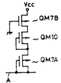
제15도는 제4실시예로서 본 발명을 EPROM에 적용시킨 경우의 반도체 기억장치를 도시해 놓은 회로도인 바, 제15도에서는 도면을 간략화하기 위해 행디코더 및 열디코더를 생략하였다. 더욱이, 간단화를 위해 메모리셀을 대표적으로 MC로서 1개만 도시하고, 열게이트 MOSFET도 BT로서 대표적으로 1개만을 도시하였다. 한편 센스증폭기(15)는 그 회로구성을 상세히 도시해 놓았는 바, 상기 실시예에서의 센스증폭기(15)는 본 회로도에 도시된 구성의 것을 사용한 것이다.FIG. 15 is a circuit diagram showing a semiconductor memory device in the case where the present invention is applied to an EPROM as a fourth embodiment. In FIG. 15, a row decoder and a column decoder are omitted in order to simplify the drawing. Furthermore, for simplicity, only one memory cell is typically represented as MC and only one column gate MOSFET is also represented as BT. On the other hand, the
본 실시예 장치가 상기 각 실시예와 실질적으로 다른 점은 제1부하회로(14A)가 전원전압(Vcc)과 노드A의 사이에 직렬접속된 2개의 P챈널 MOS트랜지스터(QM7A, QM7B)로 구성되고, 마찬가지로 제2부하회로(14B)가 전원전압(VCC)과 노드 B의 사이에 직렬접속된 2개의 P챈널 MOS트랜지스터(QD7A, QD7B)로 구성되어 있다는 것이다. 그리고, 상기 양 부하회로(14A, 14B)내의 MOS트랜지스터(QM7A, QD7A)의 게이트는 노드(A 또는 B)에 접속되고, MOS트랜지스터(QM7B, QD7B)의 게이트는 접지되어 있다.The present embodiment is substantially different from the above embodiments in that the
상기 양 부하회로(14A, 14B)에 있어서, MOS트랜지스터(QM7A, QD7A)의 각각의 크기는 동일하고, 또 MOS트랜지스터(QM7B, QD7B)의 각각의 크기도 충분히 크게 설정되어 있다. 즉, MOS트랜지스터(QM7A, QD7A)의 전류구동능력은 MOS트랜지스터(QM7B, QD7B)의 전류구동능력 보다도 크게 되어 있다.In both of the
특히, 제1부하회로(14A)내의 MOS트랜지스터(QM7B)의 크기는 메모리 셀에 소정의 전류가 흐를때에 노드A의 전위가 소저의 "0"레벨전위, 예컨대 1V정도로 되도록 설정되어 있고 또, 제2부하회로(14B)내의 MOS트랜지스터(QD7B)의 크기는 노드B의 전위가 메모리셀에 소정의 전류가 흐를때에 노드A에 얻어지는 "0"레벨의 전위와, 메모리셀에 전류가 흐르지 않을 때에 얻어지는 "1"레벨의 전위와의 정확히 중간전위로 되도록 설정된다. 또 여기서 MOS트랜지스터의 크기의 대소는 각 MOS트랜지스터의 챈널길이(L)가 모두 동등하게 설계되면 그 챈널폭(W)의 대소에 대응하게 된다.In particular, the size of the MOS transistor QM7B in the
이와 같은 구성에 있어서, 임계전압이 낮은 메모리셀이 선택되어 그 메모리셀이 도통되게 됨으로써 소정의 전류가 흐를 때에는 부하회로(14A)의 MOS트랜지스터(QM7B)의 크기가 MOS트랜지스터(QM7A)보다도 작게 설정되어 있기 때문에 부하회로(14A)의 도통 저항은 MOS트랜지스터(QM7B)에 의해 실질적으로 결정된다.In such a configuration, when a memory cell having a low threshold voltage is selected and the memory cell is turned on so that a predetermined current flows, the size of the MOS transistor QM7B of the
임계전압이 낮은 메모리셀의 다음에 임계전압이 높은 메모리셀이 선택되게 되면, 그 임계전압이 높은 메모리셀은 비도통상태로 되기 때문에 노드A의 전위는 "0"레벨로부터 상승하기 시작한다. 그리고 노드A의 전위가 "1"레벨(Vcc-P챈널 트랜지스터의 임계전압)근방으로 되면, 부하회로(14A)내의 MOS트랜지스터(QM7A)의 도통저항이 커지게 된다.When a memory cell with a high threshold voltage is selected next to a memory cell with a low threshold voltage, the potential of the node A starts to rise from the "0" level because the memory cell with the high threshold voltage is turned off. When the potential of the node A is near the " 1 " level (threshold voltage of the Vcc-P channel transistor), the conduction resistance of the MOS transistor QM7A in the
이와같이, 본 실시예에서는 노드A의 전위가 낮게 될때는 부하회로(14A)에서의 도통저항의 값은 MOS트랜지스터(QM7B)에 의해 실질적으로 결정되고, 노드A의 전위가 상승하게 되면 부하회로(14A)의 도통저항은 값은 MOS트랜지스터(QM7A)에 의해 실질적으로 결정된다.As described above, in this embodiment, when the potential of the node A becomes low, the value of the conduction resistance in the
또, 센스증폭기(15)는 P챈널 MOS트랜지스터(Q21, Q22) 및 N챈널 MOS트랜지스터(Q23∼Q27)로 이루어져 있는데, 여기서 트랜지스터(Q21, Q22)는 전류미러회로를 구성하고 있고, 트랜지스터(Q23, Q24)는 차동증폭기를 구성하고 있다. 이 차동증폭기는 트랜지스터(Q26, Q27)에 의해 생성되는 바이어스전압이 게이트에 공급되는 트랜지스터(Q25)를 통해서 접지되어 있다.The
제16도는 제15도에 도시된 반도체 기억장치에서의 부하회로(14A)의 전압-전류특성을 도시해 놓은 도면으로, 제16도에 있어서, 횡축은 노드A의 전위(Vin)를 나타내고 종축은 부하회로로 흐르는 전류를 나타낸다.FIG. 16 is a diagram showing the voltage-current characteristics of the
또, "1"레벨데이터의 기억셀이 선택되어 메모리셀에 Icell인 셀전류가 흐르는 때의 노드A의 전위가 Vin ("1"레벨), "0"레벨데이터의 기억셀이 선택된 때의 노드A의 전위가 Vin("0"레벨), 노드 B의 전위가 Vref로 도시되어 있다.The node when the potential of the node A is selected when the memory cell of "1" level data is selected and the cell current of Icell flows through the memory cell is Vin ("1" level), and the memory cell of "0" level data is selected. The potential of A is shown as Vin ("0" level) and the potential of node B is shown as Vref.
또한, 도면중의 실선이 제15도에 도시된 반도체 기억장치에서의 부하회로의 전압전류특성을 나타낸 것이고, 점선은 제1도에 도시된 종래 반도체 기억장치에서의 부하회로의 전압-전류특성을 나타낸 것이다.The solid line in the figure shows the voltage and current characteristics of the load circuit in the semiconductor memory device shown in FIG. 15, and the dotted line shows the voltage-current characteristics of the load circuit in the conventional semiconductor memory device shown in FIG. It is shown.
제16도에 도시된 바와 같이 "1"레벨데이터의 기억셀이 선택되어 소정의 메모리셀전류(Icell)가 흐를 때의 노드A의 전위[Vin("1"레벨)]는 종래 반도체 기억장치에서의 노드A의 전위와 일치한다. 그러나, 노드A의 전위(Vin)가 상승하게 되면 부하회로(14A)는 종래 반도체 기장치의 경우보다도 많은 부하전류를 흘릴 수 있게 된다.As shown in FIG. 16, the potential Vin ("1" level) of the node A when a memory cell of "1" level data is selected and a predetermined memory cell current Icell flows is determined in a conventional semiconductor memory device. Matches the potential of node A. However, when the potential Vin of the node A rises, the
이 때문에 비트선(BL)이 충전되어 노드A의 전위(in)가 ViN("1"레벨)로부터 상승할 때에는 종래의 회로 보다도 빠르게 Vin의 레벨이 상승하기 때문에 고속으로 데이터를 독출할 수 있게 된다. 그리고 노드A의 전위(Vin)가 노드B의 전위(Vref) 이상으로 되면 종래 회로의 경우와 거의 마찬가지로 부하회로(14A)에서의 MOS트랜지스터(QM7A)의 도통저항이 증가하여 부하전류는 급격히 감소하는 특성을 나타낸다.For this reason, when the bit line BL is charged and the potential A of the node A rises from ViN ("1" level), the level of Vin rises faster than that of the conventional circuit, and thus data can be read at high speed. . When the potential Vin of the node A becomes equal to or higher than the potential Vref of the node B, the conduction resistance of the MOS transistor QM7A in the
제17도는 상기 제15도에 도시된 회로에 있어서, 비트선을 절환해서 임계전압이 낮은 메모리셀의 다음에 임계전압이 높은 메모리셀을 선택한 경우의 노드A의 전류변화를 도시해 놓은 특성도이다. 또한, 제1도에 도시된 회로와 비교하기 위해 제1도의 회로에 대한 특성을 점선으로 도시해 놓았다.FIG. 17 is a characteristic diagram showing a change in current of the node A when the bit line is switched and a memory cell having a high threshold voltage is selected next to the memory cell having a low threshold voltage in the circuit shown in FIG. . In addition, the characteristics of the circuit of FIG. 1 are shown in dotted lines for comparison with the circuit shown in FIG.
우선, 시각 t0에서 입력어드레스가 절환되고, 그 후 시각 t1에서 새로운 비트선(BL)이 선택된다. 이 시각 t1까지는 임계전압이 낮은 메모리셀이 선택되기 때문에 노드A의 전위는 Vin("1"레벨)으로 된다.First, the input address is switched at time t0, and then a new bit line BL is selected at time t1. Until this time t1, the memory cell having a low threshold voltage is selected, so that the potential of the node A becomes Vin ("1" level).
그리고, 시각 t1에서 임계전압이 높은 메모리셀이 접속된 새로운 비트선으로 절환되면, 비트선(BL)은 바이어스전위 설정회로(13A)내의 MOS트랜지스터(QM4)를 통해서 급속히 충전되고, 그 사이 노드A의 전위(Vin)는 일단 Vin("1"레벨)보다 낮아지게 된다.When the memory cell with a high threshold voltage is switched to a new bit line connected at time t1, the bit line BL is rapidly charged through the MOS transistor QM4 in the bias
이어, 시각 t2에서 노드A의 전위(Vin)가 노드 B의 전위(Vref)이상으로 되면, 센스증폭기(15)의 출력레벨이 반전하여 독출되는 메모리셀의 논리"0"데이터가 출력된다.Then, when the potential Vin of the node A becomes equal to or higher than the potential Vref of the node B at time t2, the logic " 0 " data of the memory cell read out by inverting the output level of the
제1도에 도시된 종래 회로의 경우에는 도면에 점선으로 도시된 바와 같이 시각 t2보다도 지연된 시각 t3에서 노드A의 전위(Vin)가 노드B의 전위(Vref)이상으로 되고, 이 시점에서 센스증폭기(15)의 출력레벨이 반전하여 데이터가 출력된다.In the conventional circuit shown in FIG. 1, the potential Vin of the node A becomes equal to or greater than the potential Vref of the node B at a time t3 delayed from the time t2 as shown by the dotted line in the figure. The output level of (15) is inverted to output data.
이와 같이 제15도에 도시된 회로에서는 도통상태의 메모리셀이 선택된때의 노드A의 전위(Vin)와 노드 B의 전위(Vref)를 종래 회로와 동일한 값으로 설정한 경우에, 제3도에 도시된 종래 회로의 경우보다도 (t3-t2)의 시간만큼 데이터 독출동작을 고속화할 수 있게 된다.Thus, in the circuit shown in FIG. 15, in the case where the potential Vin of the node A and the potential Vref of the node B when the memory cell in the conductive state is selected are set to the same values as in the conventional circuit, FIG. The data read operation can be made faster by the time (t3-t2) than in the conventional circuit shown in the figure.
더욱이 제15도에 도시된 본 실시예에 따른 회로에 의하면 "0"데이터 출력시에 전원전압이 변동해도 오동작을 발생을 방지할 수 있게 되고, 전원노이즈 마진을 확장 할 수 있게 된다.Furthermore, according to the circuit according to the present embodiment shown in FIG. 15, malfunction can be prevented even if the power supply voltage fluctuates at the time of " 0 " data output, and the power supply noise margin can be extended.
일반적으로, 출력버퍼회로의 출력에 접속되는 외부출력 용량을 충·방전할때에 전원전압의 변동이 발생되는 데이터 독출속도가 빠른 기억 장치에서는 센스증폭기의 출력이 절환된 후부터 출력버퍼회로의 출력이 절환될때까지의 시간이 짧기 때문에 노드A와 노드B의 전위차가 충분하지 않을 때에 전원전압이 변동하게 됨으로써 오동작하기 쉽게 된다.In general, in the case of a memory device having a high data reading speed in which a change in power supply voltage occurs when charging and discharging an external output capacity connected to the output of the output buffer circuit, the output of the output buffer circuit is switched after the output of the sense amplifier is switched. Since the time until it becomes short, the power supply voltage fluctuates when the potential difference between node A and node B is not enough, and it becomes easy to malfunction.
제17도에 도시된 바와 같이 노드A의 전위(Vin)가 노드B의 전위(Vref)와 동일하게 되고 나서 △T의 시간 후에 출력버퍼회로의 출력이 절환되게 되고, 노드A의 전위 (Vin)가 노드B의 전위(Vref)와 동일하게되고 나서 △T시간후의 노드A의 전위(Vin)는 제1도에 도시된 종래 회로의 경우보다도 △V만큼 높은 것으로 된다.As shown in FIG. 17, the potential Vin of node A becomes equal to the potential Vref of node B, and after the time of ΔT, the output of the output buffer circuit is switched and the potential Vin of node A is switched. Is equal to the potential Vref of the node B, the potential Vin of the node A after ΔT time becomes higher by ΔV than in the case of the conventional circuit shown in FIG.
이 때문에 시각 t2로부터 △T시간후에 출력버퍼회로의 출력이 절환되어도 본 실시예에 다른 회로에서는 노드A의 전위(Vin)가 충분히 높게 되므로, 출력버퍼회로의 출력이 절환되어 전원전압이 변동하더라도 오동작발생을 방지할 수 있게 되고, 그 결과 반도체 기억장치의 전원 노이즈마진을 크게 할 수 있게 된다.Therefore, even if the output of the output buffer circuit is switched after the time T2 from time t2, the potential Vin of the node A is sufficiently high in the other circuits according to the present embodiment. Thus, even if the output of the output buffer circuit is switched and the power supply voltage changes, malfunction It is possible to prevent the occurrence, and as a result, it is possible to increase the power supply noise margin of the semiconductor memory device.
즉, 제15도에 도시된 상기 실시예에 의하면, 고속으로 데이터를 독출할 수 있게 되고, 또 높은 전원 노이즈마진을 갖는 반도체 기억장치를 실현할 수 있게 된다.That is, according to the embodiment shown in FIG. 15, data can be read at high speed and a semiconductor memory device having a high power supply noise margin can be realized.
제18도는 본 발명의 제5실시예에 따른 반도체 기억장치를 도시해 놓은 회로도로서, 상기 제15도에 도시된 회로와 마찬가지로 메모리셀로서 부유게이트와 제어게이트의 2층 게이트구조를 갖는 MOS트랜지스터를 사용한 EPROM에 본 발명을 실시한 것이다. 단 본 실시예에서는 제15도에 도시된 회로와 동일한 부분에는 동일 참조부호를 붙이고, 그에 대한 상세한 설명은 생략한다.FIG. 18 is a circuit diagram showing a semiconductor memory device according to a fifth embodiment of the present invention. Similar to the circuit shown in FIG. 15, a MOS transistor having a double-layer gate structure of floating gate and control gate is used as a memory cell. This invention is implemented to the used EPROM. However, in the present embodiment, the same reference numerals are given to the same parts as the circuit shown in FIG. 15, and detailed description thereof will be omitted.
본 실시예에서는 제1 및 제2부하회로(14A, 14B)내의 MOS트랜지스터(QM7B, QD7B)의 게이트를 접지시키는 대신에 양 게이트에 제어신호![]()
![]()
이 제어신호![]()
![]()
![]()
![]()
![]()
![]()
본 실시예에 따른 반도체 기억장치가 활성상태인 때에는 제어신호![]()
![]()
![]()
![]()
제19a도 내지 제19c도는 각각 제15도 및 제18도에 도시된 회로에서 사용되는 제1부하회로(14A)의 다른 구성예를 도시해 놓은 회로도이다.19A to 19C are circuit diagrams showing another example of the configuration of the
제19a도에 도시된 부하회로는 제15도에 도시된 회로에서의 P챈널 MOS트랜지스터(QM7B) 대신에 임계전압이 부(-)의 값을 갖는 디플리이션형 N챈널 MOS트랜지스터(QM8)를 이용하도록 된 것이다. 그리고, 이 MOS트랜지스터(QM8)의 게이트는 그 소오스에 접속되어 있다.The load circuit shown in FIG. 19A replaces the P-channel MOS transistor QM7B in the circuit shown in FIG. 15 with a deflection type N-channel MOS transistor QM8 having a negative threshold voltage. It is to be used. The gate of this MOS transistor QM8 is connected to the source thereof.
이 MOS트랜지스터(QM8)는 게이트가 소오스에 접속되어 있기 때문에 상기 P챈널 MOS트랜지스터(QM7B)와 마찬가지로 노드A의 전위가 낮아지게 되면 정전류부하특성을 나타내므로 동일한 효과를 얻을 수 있게 된다.Since the gate of the MOS transistor QM8 is connected to the source, similar to the P-channel MOS transistor QM7B, when the potential of the node A is lowered, the MOS transistor QM8 exhibits a constant current load characteristic, thereby achieving the same effect.
또, MOS트랜지스터(QM8)의 도통저항은 상기 메모리셀에 소정의 전류가 흐를 때에 노드A의 전위(Vin)가 소정의 값, 예컨대 1V로 되도록 설정된다.The conduction resistance of the MOS transistor QM8 is set so that the potential Vin of the node A becomes a predetermined value, for example, 1V when a predetermined current flows in the memory cell.
제19b도에 도시된 부하회로는 제15도에 도시된 회로에서의 P챈널 MOS트랜지스터(QM7A) 대신에 게이트가 전원전압(Vcc)에 접속된 인핸스먼트형 N챈널 MOS트랜지스터(QM9)를 이용하고, 제15도에 도시된 회로에서의 P챈널 MOS트랜지스터(QM7B) 대신에 임계전압이 부(-)의 값을 갖는 디플리션형 N챈널 MOS트랜지스터(QM8)를 이용하도록 된 것으로, 여기서 MOS트랜지스터(QM9)의 도통저항은 MOS트랜지스터(QM8)의 도통저항보다 크게 설정되어 있기 때문에 제16도에 도시된 바와 같은 전압-전류특성을 얻을 수 있게 된다.The load circuit shown in FIG. 19B uses an enhancement N-channel MOS transistor QM9 whose gate is connected to the power supply voltage Vcc instead of the P-channel MOS transistor QM7A in the circuit shown in FIG. Instead of the P-channel MOS transistor QM7B in the circuit shown in FIG. 15, a depletion-type N-channel MOS transistor QM8 whose threshold voltage has a negative value is used, where the MOS transistor ( Since the conduction resistance of QM9) is set larger than the conduction resistance of MOS transistor QM8, voltage-current characteristics as shown in FIG. 16 can be obtained.
그리고, 상기 MOS트랜지스터(QM8)의 도통저항의 값은 상기 메모리셀에 소정 전류가 흐를 때에 노드A가 소정의 전위로 되도록 설정되어 있다.The value of the conduction resistance of the MOS transistor QM8 is set so that the node A becomes a predetermined potential when a predetermined current flows through the memory cell.
이 제19b도에 도시된 부하회로를 사용함으로써, 임계전압이 높은 메모리셀이 선택된 때의 노드A의 전위는 전원전압(Vcc)보다 N챈널 MOS트랜지스터(QM8)의 임계전압 만큼 낮은 값으로 설정되고, 또 MOS 트랜지스터를 N챈널 MOS트랜지스터로 구성할 수 있게 됨으로써 본 발명의 반도체 기억장치를 저가의 N챈널 MOS형 집적회로로 실현할 수 있게 된다.By using the load circuit shown in FIG. 19B, the potential of the node A when the memory cell having a high threshold voltage is selected is set to a value lower than the power supply voltage Vcc by the threshold voltage of the N-channel MOS transistor QM8. In addition, since the MOS transistor can be configured by an N-channel MOS transistor, the semiconductor memory device of the present invention can be realized as an inexpensive N-channel MOS integrated circuit.
제19c도에 도시된 부하회로는 제15도에 도시된 회로에서의 P챈널 MOS트랜지스터(QM7A, QM7B)사이에 P챈널 MOS트랜지스터(QM10)를 접속해서 구성한 것으로, 이 MOS트랜지스터(QM10)의 도통저항도 MOS트랜지스터(QM7A)와 마찬가지로 MOS트랜지스터(QM7B)에 비해 크게 설정되고, 또 이 MOS트랜지스터(QM10)의 게이트는 드레인에 접속되어 있다.The load circuit shown in FIG. 19C is formed by connecting P channel MOS transistors QM10 between the P channel MOS transistors QM7A and QM7B in the circuit shown in FIG. 15, and the conduction of the MOS transistor QM10 is performed. Similarly to the MOS transistor QM7A, the resistance is set larger than that of the MOS transistor QM7B, and the gate of the MOS transistor QM10 is connected to the drain.
그리고, 이 MOS트랜지스터(QM10)를 직렬로 삽입함으로써 임계전압이 높은 메모리셀이 선택된 때의 노드A의 전위는 전원전압(Vcc)보다 P챈널 MOS트랜지스터 2개분의 임계전압 만큼 낮아지도록 제어된다.By inserting the MOS transistors QM10 in series, the potential of the node A when the memory cell having a high threshold voltage is selected is controlled to be lower by the threshold voltage of two P-channel MOS transistors than the power supply voltage Vcc.
또, 이 부하회로를 사용함으로써 노드A의 진폭레벨을 낮추는 것이 가능해지게 되고, 회로임계전압이 낮은 센스증폭기를 이용한 경우에도 고속동작을 실현할 수 있게 된다.By using this load circuit, the amplitude level of the node A can be reduced, and high-speed operation can be realized even when a sense amplifier having a low circuit threshold voltage is used.
또한, 상기 제19a도 내지 제19c도에 도시된 바와 같은 구성의 제1부하회로(14A)를 사용하는 경우에는 디바이스의 특성을 고려해서 제2부하회로(14B)도 이것과 동일한 구성의 것을 사용해도 된다.In addition, when using the
또한, 이때 트랜지스터(QM8)의 크기를 상기와 같은 조건, 즉 노드B의 전위(Vref)가 메모리셀에 소정의 전류가 흐를때에 노드A에서 얻어지는 "0"레벨의 전위와, 메모리셀에 전류가 흐르지 않을 때에 노드A에 얻어지는 "1"레벨의 전위의 정확히 중간전위로 되도록 관계를 만족시켜 설정하는 것이 필요하다.In this case, the size of the transistor QM8 is set to the same condition as that described above, that is, the potential Vref of the node B is obtained at the node A when a predetermined current flows in the memory cell, and the current in the memory cell. When is not flowing, it is necessary to satisfy and set the relationship so that the potential of the " 1 " level obtained at the node A becomes exactly an intermediate potential.
또, 본 발명은 상기 실시예에 한정되지 않고, 여러가지로 변형시켜 실시할 수 있다. 예를들어, 상기 각 실시예에서는 센스증폭기로서 전류미러형 센스증폭기를 이용하는 경우에 대해 설명했지만, 이것은 예컨대 인버터형 센스증폭기를 사용해도 상기와 같이 고속으로 전원노이즈에 강한 반도체 기억장치를 실현할 수 있다. 또, 상기 실시예에서는 메모리셀에 소정의 전류가 흐를 때, 노드A의 전위가 소정값이 되도록 설정하게 되는 MOS트랜지스터, 예컨대 제15도에 도시된 MOS트랜지스터(QM7)등의 도통저항을 챈널폭(W)으로 조정하는 경우에 대해서 설명했지만, 이것은 접지전위를 게이트에 공급하거나, 게이트에 소정 바이어스전압을 공급함으로써 도통저항의 값을 설정해도 된다.In addition, this invention is not limited to the said Example, It can variously deform and implement. For example, in each of the above embodiments, the case where the current mirror type sense amplifier is used as the sense amplifier has been described. However, even when the inverter type sense amplifier is used, the semiconductor memory device resistant to power supply noise at high speed can be realized as described above. . In the above embodiment, when a predetermined current flows through the memory cell, the channel width of the conductive resistance of the MOS transistor, for example, the MOS transistor QM7 shown in FIG. 15, is set so that the potential of the node A becomes a predetermined value. Although the case of adjusting to (W) has been described, this may be set by supplying a ground potential to the gate or by supplying a predetermined bias voltage to the gate.
또, 상기 각 실시예에서는 메모리셀로서 2층게이트구조를 갖는 불휘발성 트랜지스터를 사용하는 불휘발성 반도체 기억장치에 본 발명을 적용시킨 경우에 대해서 설명했지만, 본 발명은 1층게이트구조의 MOS트랜지스터를 메모리셀로서 사용하고, 제조공정중에 챈널영역에 선택적으로 이온주입을 행함으로써 임계전압을 높이거나 낮추게 되는 마스크 ROM에도 실시할 수 있다.Incidentally, in the above embodiments, the case where the present invention is applied to a nonvolatile semiconductor memory device using a nonvolatile transistor having a two-layer gate structure as a memory cell has been described. However, the present invention provides a MOS transistor having a one-layer gate structure. It can also be used as a mask cell, which is used as a memory cell and selectively or ionically implanted into the channel region during the manufacturing process to raise or lower the threshold voltage.
제15도 내지 제19도에 도시된 각 실시예에 의하면, 부하회로를 메모리셀이 도통되어 데이터 검출노드전위가 낮을 때에는 거의 정전류특성을 나타내는 제1부하수단과, 메모리셀이 비도통상태로 될 때에는 데이터검출노드의 전위를 전원전압보다도 소정 값만큼 낮은 값으로 설정하는 제2부하수단이 직렬접속된 구성으로 하게 되므로, 노이즈에 대한 전원전압의 변동에 대해서 높은 동작마진을 갖는 한편, 동작속도의 고속화를 용이하게 도모할 수 있도록 된 반도체 기억장치를 제공할 수 있게 된다.According to each of the embodiments shown in Figs. 15 to 19, the load circuit has a first load means exhibiting almost constant current characteristics when the memory cell is turned on and the data detection node potential is low, and the memory cell is brought into a non-conductive state. In this case, since the second load means for setting the potential of the data detection node to a value lower than the power supply voltage by a predetermined value is configured in series, it has a high operating margin against fluctuations in the power supply voltage to noise and It is possible to provide a semiconductor memory device capable of easily speeding up.
제20도 및 제21도는 본 발명의 제6 및 제7실시예에 따른 반도체 기억장치를 도시한 것인 바, 제20도에 도시된 실시예는 제7도에 도시된 실시예와 제15도에 도시된 실시예를 조합시킨 것으로, 즉 더미비트선(DBL)에 그 게이트가 Vcc에 접속된 더미셀(DCm+1)을 설치함과 더불어, 부하회로(14A, 14B)를 각각 직렬접속된 MOSFET(QM7A, QM7B), (QD7A, QD7B)로 구성한 것이다.20 and 21 show a semiconductor memory device according to the sixth and seventh embodiments of the present invention. The embodiment shown in FIG. 20 is the embodiment shown in FIG. In the embodiment shown in Fig. 1, that is, the dummy cell DCm + 1 having its gate connected to Vcc is provided on the dummy bit line DBL, and the
또한, 제21도에 도시된 실시예는 제12도에 도시된 실시예와 제18도에 도시된 실시예를 조합시킨 것으로, 즉 ATD(18)로부터의 펄스출력이 그 게이트에 인가되는 더미셀(DCm+1)을 더미비트선(DBC)에 설치함과 더불어, 제1 및 제2부하회로(14A, 14B)를 각각 직렬접속된 MOSFET(QM7A, QM7B), (QD7A, QD7B)로 구성시킨 것이다.Further, the embodiment shown in FIG. 21 combines the embodiment shown in FIG. 12 with the embodiment shown in FIG. 18, that is, a dummy cell to which a pulse output from the ATD 18 is applied to its gate. In addition to providing (DCm + 1) to the dummy bit line DBC, the first and
제20도 및 제21도에 도시된 실시예에서 부하회로(14A, 14B)는 제19a도 내지 제19c도에 도시된 구성으로 해도 된다.In the embodiment shown in Figs. 20 and 21, the
제20도 및 제21도에 도시된 실시예의 동작은 각각 제7도에 도시된 실시예의 동작과 제15도에 도시된 실시예의 동작을 조합시키거나, 제12도에 도시된 실시예의 동작과 제18도에 도시된 실시예의 동작을 조합시키면 되므로 그 동작설명은 생략한다.The operation of the embodiment shown in FIGS. 20 and 21 combines the operation of the embodiment shown in FIG. 7 with the operation of the embodiment shown in FIG. 15, respectively, or the operation of the embodiment shown in FIG. Since operation of the embodiment shown in FIG. 18 is combined, the operation description thereof will be omitted.
그리고, 본 실시예에 의해서 워드선의 선택이 절환되는 과도기간에도 기준전위(Vref)의 상승이 억제되고, 전원에 노이즈가 발생되지 않게될 뿐 아니라 전원전압의 변동에 대해 높은 마진을 갖게 됨으로써 동작 속도의 향상을 도모할 수 있게 된다.In this embodiment, the increase of the reference potential Vref is suppressed even in the transient period in which the selection of the word line is switched, not only the noise is generated in the power supply, but also a high margin for the fluctuation of the power supply voltage. It can be improved.
제22도는 본 발명의 제8실시예에 따른 반도체 기억장치를 도시해 놓은 회로도로서, 제18도에 도시된 회로에서의 바이어스전위 설정회로(13A, 13B)의 정전위발생회로 대신에 비트선전위에 따라 출력전위가 변화되는 피드백형 바이어스발생회로를 사용한 것이다.FIG. 22 is a circuit diagram showing a semiconductor memory device according to an eighth embodiment of the present invention, in which a bit line potential is used instead of the electrostatic potential generating circuits of the bias
제22도에 도시된 바와 같이 바이어스전위 설정회로(13A)의 N챈널 MOS트랜지스터(QM5, QM6)로 구성되는 정전위발생회로는 각각 게이트가 열게이트 트랜지스터(BT)의 드레인에 접속된 P챈널 MOS트랜지스터(QM5)와 N챈널 MOS트랜지스터(QM6)로 치환되어 있고, 또 N챈널 MOS트랜지스터(QM2), (QM3)로 구성되는 정전위발생회로도 각각 그 게이트가 상기 열게이트 트랜지스터(BT)의 드레인에 접속되는 P챈널 MOS트랜지스터(QM2)와 N챈널 MOS트랜지스터(QM3)로 치환되어 있다. 또, 바이어스전위 설정회로(13B)도 상기 바이어스전위 설정회로(13A)와 동일하게 변경되어 P챈널 MOS트랜지스터(QD2, QD5) 및 N챈널 트랜지스터(QD3, QD6)의 게이트는 N챈널 MOS트랜지스터(DBT)의 드레인에 접속되어 있다.As shown in FIG. 22, in the electrostatic potential generating circuit composed of the N-channel MOS transistors QM5 and QM6 of the bias
이와 같이 구성된 바이어스전위 설정회로를 사용하게 되면, 비트선 전위의 미소한 진폭에 대해서 노드A의 전위(Vin)가 크게 변화되기 때문에 데이터 독출속도가 고속화된다. 제22도에 도시된 바와 같이, 본 발명에 따른 부하회로(14A)를 이와 같은 피드백형 바이어스회로가 사용된 불휘발성 반도체 기억장치에 응용함으로써 보다 고속으로 동작되는 불휘발성 반도체 기억장치를 실현할 수 있게 된다.By using the bias potential setting circuit configured in this way, the potential Vin of the node A is greatly changed with respect to the minute amplitude of the bit line potential, thereby speeding up the data reading speed. As shown in Fig. 22, by applying the
또한, 이와 마찬가지로 제7도에 도시된 회로에서의 바이어스전위 설정회로(13A, 13B)를 제22도에 도시된 피드백형 바이어스회로로 치환함으로써 전원노이즈로 인한 오동작이 발생되지 않는 불휘발성 반도체 기억장치를 실현할 수 있게 된다.Similarly, by replacing the bias
한편, 본원 청구범위의 각 구성요소에 병기된 도면참조부호는 본원 발명의 이해를 용이하게 하기 위한 것으로, 본원 발명의 기술적 범위를 도면에 도시한 실시예로 한정할 의도에서 병기한 것은 아니다.On the other hand, reference numerals denoted in the components of the claims of the present application to facilitate the understanding of the present invention, not intended to limit the technical scope of the present invention to the embodiments shown in the drawings.
Claims (27)
Applications Claiming Priority (6)
| Application Number | Priority Date | Filing Date | Title |
|---|---|---|---|
| JP15653988A JPH07109719B2 (en) | 1988-06-24 | 1988-06-24 | Semiconductor memory device |
| JP63-156539 | 1988-06-24 | ||
| JP88-156539 | 1988-06-24 | ||
| JP88-161344 | 1988-06-29 | ||
| JP16134488A JPH0642320B2 (en) | 1988-06-29 | 1988-06-29 | Semiconductor memory device |
| JP63-161344 | 1988-06-29 |
Publications (2)
| Publication Number | Publication Date |
|---|---|
| KR910001750A KR910001750A (en) | 1991-01-31 |
| KR930001735B1 true KR930001735B1 (en) | 1993-03-12 |
Family
ID=26484252
Family Applications (1)
| Application Number | Title | Priority Date | Filing Date |
|---|---|---|---|
| KR1019890008749A KR930001735B1 (en) | 1988-06-24 | 1989-06-24 | Semiconductor memory device |
Country Status (4)
| Country | Link |
|---|---|
| US (1) | US5040148A (en) |
| EP (3) | EP0576046B1 (en) |
| KR (1) | KR930001735B1 (en) |
| DE (3) | DE68923588T2 (en) |
Families Citing this family (21)
| Publication number | Priority date | Publication date | Assignee | Title |
|---|---|---|---|---|
| US5191552A (en) * | 1988-06-24 | 1993-03-02 | Kabushiki Kaisha Toshiba | Semiconductor memory device with address transition actuated dummy cell |
| US5276643A (en) * | 1988-08-11 | 1994-01-04 | Siemens Aktiengesellschaft | Integrated semiconductor circuit |
| JPH03156795A (en) * | 1989-11-15 | 1991-07-04 | Toshiba Micro Electron Kk | Semiconductor memory circuit device |
| IT1246241B (en) * | 1990-02-23 | 1994-11-17 | Sgs Thomson Microelectronics | CIRCUIT FOR READING THE INFORMATION CONTAINED IN NON-VOLATILE MEMORY CELLS |
| EP0487808B1 (en) * | 1990-11-19 | 1997-02-19 | STMicroelectronics S.r.l. | Memories with unbalanced loads and with compensation |
| KR940005688B1 (en) * | 1991-09-05 | 1994-06-22 | 삼성전자 주식회사 | Automatic precharge detecting device of the data line in memory element |
| JPH0574181A (en) * | 1991-09-10 | 1993-03-26 | Nec Corp | Data readout circuit of semiconductor memory device |
| JP3397427B2 (en) * | 1994-02-02 | 2003-04-14 | 株式会社東芝 | Semiconductor storage device |
| US5390147A (en) * | 1994-03-02 | 1995-02-14 | Atmel Corporation | Core organization and sense amplifier having lubricating current, active clamping and buffered sense node for speed enhancement for non-volatile memory |
| DE69424771T2 (en) * | 1994-03-22 | 2000-10-26 | St Microelectronics Srl | Arrangement for reading a memory cell matrix |
| DE69427461T2 (en) * | 1994-03-31 | 2002-04-11 | St Microelectronics Srl | Non-volatile memory element with double programmable cell and corresponding read circuit for redundancy circuit |
| GB9423034D0 (en) * | 1994-11-15 | 1995-01-04 | Sgs Thomson Microelectronics | A reference circuit |
| JPH08221996A (en) * | 1995-02-17 | 1996-08-30 | Nec Corp | Semiconductor storage |
| JP3734550B2 (en) * | 1996-01-30 | 2006-01-11 | 株式会社ルネサステクノロジ | Semiconductor memory device |
| DE69630672D1 (en) * | 1996-03-29 | 2003-12-18 | St Microelectronics Srl | Reference system for determining the programming / non-programming state of a memory cell, in particular for non-volatile memories |
| US5602788A (en) * | 1996-06-07 | 1997-02-11 | International Business Machines Corporation | Read only memory having localized reference bit lines |
| US5729493A (en) * | 1996-08-23 | 1998-03-17 | Motorola Inc. | Memory suitable for operation at low power supply voltages and sense amplifier therefor |
| DE69905699T2 (en) * | 1999-06-21 | 2003-10-16 | St Microelectronics Srl | Read process for non-volatile memories with a sampling current variable with the read voltage, and arrangement for realizing this process |
| TW559814B (en) * | 2001-05-31 | 2003-11-01 | Semiconductor Energy Lab | Nonvolatile memory and method of driving the same |
| JP2003077282A (en) * | 2001-08-31 | 2003-03-14 | Fujitsu Ltd | Nonvolatile semiconductor memory |
| KR100454145B1 (en) * | 2001-11-23 | 2004-10-26 | 주식회사 하이닉스반도체 | Flash memory device |
Family Cites Families (10)
| Publication number | Priority date | Publication date | Assignee | Title |
|---|---|---|---|---|
| JPS53117341A (en) * | 1977-03-24 | 1978-10-13 | Toshiba Corp | Semiconductor memory |
| EP0122564B1 (en) * | 1983-04-07 | 1990-07-18 | Kabushiki Kaisha Toshiba | Read only memory |
| JPH0666115B2 (en) * | 1983-09-26 | 1994-08-24 | 株式会社東芝 | Semiconductor memory device |
| JPS60150297A (en) * | 1984-01-13 | 1985-08-07 | Nec Corp | Memory |
| US4805143A (en) * | 1986-01-16 | 1989-02-14 | Hitachi Ltd. | Read-only memory |
| JPS62197996A (en) * | 1986-02-24 | 1987-09-01 | Toshiba Corp | Sense amplifier for semiconductor memory |
| JPS62231500A (en) * | 1986-03-31 | 1987-10-12 | Toshiba Corp | Semiconductor storage device |
| US4819212A (en) * | 1986-05-31 | 1989-04-04 | Kabushiki Kaisha Toshiba | Nonvolatile semiconductor memory device with readout test circuitry |
| IT1213343B (en) * | 1986-09-12 | 1989-12-20 | Sgs Microelettronica Spa | DETECTION CIRCUIT OF THE STATE OF MATRIX CELLS IN EPROM MEMORIES IN MOS TECHNOLOGY. |
| JP2507529B2 (en) * | 1988-03-31 | 1996-06-12 | 株式会社東芝 | Nonvolatile semiconductor memory device |
-
1989
- 1989-06-23 DE DE68923588T patent/DE68923588T2/en not_active Expired - Fee Related
- 1989-06-23 EP EP93114324A patent/EP0576046B1/en not_active Expired - Lifetime
- 1989-06-23 EP EP89111475A patent/EP0347935B1/en not_active Expired - Lifetime
- 1989-06-23 DE DE68926124T patent/DE68926124T2/en not_active Expired - Fee Related
- 1989-06-23 DE DE68923624T patent/DE68923624T2/en not_active Expired - Fee Related
- 1989-06-23 EP EP93114322A patent/EP0576045B1/en not_active Expired - Lifetime
- 1989-06-23 US US07/370,869 patent/US5040148A/en not_active Expired - Lifetime
- 1989-06-24 KR KR1019890008749A patent/KR930001735B1/en not_active IP Right Cessation
Also Published As
| Publication number | Publication date |
|---|---|
| EP0576045A3 (en) | 1994-02-16 |
| EP0347935A3 (en) | 1991-05-29 |
| EP0576045A2 (en) | 1993-12-29 |
| DE68926124D1 (en) | 1996-05-02 |
| EP0347935A2 (en) | 1989-12-27 |
| DE68923588D1 (en) | 1995-08-31 |
| DE68923624T2 (en) | 1996-02-01 |
| EP0576046B1 (en) | 1996-03-27 |
| US5040148A (en) | 1991-08-13 |
| EP0576045B1 (en) | 1995-07-26 |
| DE68923624D1 (en) | 1995-08-31 |
| KR910001750A (en) | 1991-01-31 |
| EP0576046A3 (en) | 1994-02-09 |
| EP0347935B1 (en) | 1995-07-26 |
| EP0576046A2 (en) | 1993-12-29 |
| DE68926124T2 (en) | 1996-09-19 |
| DE68923588T2 (en) | 1996-07-04 |
Similar Documents
| Publication | Publication Date | Title |
|---|---|---|
| KR930001735B1 (en) | Semiconductor memory device | |
| US6842377B2 (en) | Nonvolatile semiconductor memory device with first and second read modes | |
| US5258958A (en) | Semiconductor memory device | |
| US5197028A (en) | Semiconductor memory device with dual reference elements | |
| US7082061B2 (en) | Memory array with low power bit line precharge | |
| JPS62164300A (en) | Electrically erasable/programmable semiconductor memory cell | |
| EP0791936B1 (en) | Semiconductor memory device | |
| US5396467A (en) | Sense amplifier | |
| US5191552A (en) | Semiconductor memory device with address transition actuated dummy cell | |
| JP3532721B2 (en) | Constant voltage generator | |
| JP3615009B2 (en) | Semiconductor memory device | |
| US6163481A (en) | Flash memory wordline tracking across whole chip | |
| US20050111277A1 (en) | Non-volatile memory control techniques | |
| US20020054531A1 (en) | Non-volatile semiconductor memory device | |
| US6292406B1 (en) | Method and low-power circuits used to generate accurate boosted wordline voltage for flash memory core cells in read mode | |
| US6292399B1 (en) | Method and low-power circuits used to generate accurate drain voltage for flash memory core cells in read mode | |
| JPH10326495A (en) | Nonvolatile semiconductor memory | |
| US6704225B2 (en) | Sensing circuit for nonvolatile memory device | |
| JP3828694B2 (en) | Sensing circuit for semiconductor memory device and sensing method using the same | |
| JP2865388B2 (en) | Semiconductor storage device | |
| KR0179658B1 (en) | Semiconductor memory device | |
| KR20230056198A (en) | Circuit for Reading Data of a Memory Cell | |
| JP2595084B2 (en) | Semiconductor storage device | |
| US20020041530A1 (en) | Semiconductor memory device having driver circuit which supplies temporary accelerated charge | |
| KR930000817B1 (en) | Nonvolatile semiconductor memory device |
Legal Events
| Date | Code | Title | Description |
|---|---|---|---|
| A201 | Request for examination | ||
| G160 | Decision to publish patent application | ||
| E701 | Decision to grant or registration of patent right | ||
| GRNT | Written decision to grant | ||
| FPAY | Annual fee payment |
Payment date: 20030228 Year of fee payment: 11 |
|
| LAPS | Lapse due to unpaid annual fee |