EP0346856B1 - Verfahren und Schaltung zur Verarbeitung und Übertragung eines Taktsignals, speziell der Videosynchronisationsfrequenz - Google Patents
Verfahren und Schaltung zur Verarbeitung und Übertragung eines Taktsignals, speziell der Videosynchronisationsfrequenz Download PDFInfo
- Publication number
- EP0346856B1 EP0346856B1 EP89110730A EP89110730A EP0346856B1 EP 0346856 B1 EP0346856 B1 EP 0346856B1 EP 89110730 A EP89110730 A EP 89110730A EP 89110730 A EP89110730 A EP 89110730A EP 0346856 B1 EP0346856 B1 EP 0346856B1
- Authority
- EP
- European Patent Office
- Prior art keywords
- fsr
- clock signal
- error
- jitter
- circuit
- Prior art date
- Legal status (The legal status is an assumption and is not a legal conclusion. Google has not performed a legal analysis and makes no representation as to the accuracy of the status listed.)
- Expired - Lifetime
Links
- 238000000034 method Methods 0.000 title claims description 11
- 230000005540 biological transmission Effects 0.000 title description 4
- 230000007704 transition Effects 0.000 claims description 8
- 238000005259 measurement Methods 0.000 claims description 3
- 238000005070 sampling Methods 0.000 description 3
- 230000000295 complement effect Effects 0.000 description 1
- 230000006835 compression Effects 0.000 description 1
- 238000007906 compression Methods 0.000 description 1
- 238000010586 diagram Methods 0.000 description 1
- 230000010354 integration Effects 0.000 description 1
- 230000000630 rising effect Effects 0.000 description 1
- 229920006395 saturated elastomer Polymers 0.000 description 1
- 230000001629 suppression Effects 0.000 description 1
Images

Classifications
-
- H—ELECTRICITY
- H04—ELECTRIC COMMUNICATION TECHNIQUE
- H04N—PICTORIAL COMMUNICATION, e.g. TELEVISION
- H04N5/00—Details of television systems
- H04N5/04—Synchronising
- H04N5/06—Generation of synchronising signals
- H04N5/067—Arrangements or circuits at the transmitter end
Definitions
- the invention refers to a method and circuit for processing and transmitting a clock signal having a period 1/Fsr and being affected by jitter, wherein the period of the clock signal is measured by means of a sample signal having a frequency Fc.
- the invention is particularly applicable to the video synchronisation signal.
- a comparison is performed between such frequency value and a sample frequency that is known also at the receiver.
- the sample frequency is related to the frequency at which the data are transmitted.
- EP-A-0,126,586 discloses a circuit for synchronizing a television input frame pulse with a reference frame pulse by generating a reverse frame pulse, which is applied to a television signal processor for adjusting the phase of the television signal passed therethrough.
- the operation of this known circuit is thus similar to method (2) above.
- the present invention is based on method (3) above, but requires the transmission of minimum information only, i.e. just one single bit for each individual period, while taking account of the jitter in the frequency of the clock signal (which may be a video signal).
- the ratio Fc/Fsr between the frequency of the sample signal and that of the clock signal is a decimal number of the form n.m, i.e. a number between n and n+1. It is therefore possible to convert the single measured value to an integer equal to n or n+1. This can be done for instance by means of a circuit that detects the rising (or falling) slopes of the clock signal having the frequency Fsr, and initializes a counter at the value 0. This counter, which operates at the frequency Fc of the sample signal, thus provides a measured value, i.e. the final count, which is either n or n+1.
- the transmission is done by, e.g., transmitting a "0" in case the final count is n, and a "1" in case the final count is n+1.
- the measured value or count can have values other than n and n+1.
- the invention instead of transmitting the actual measured value of the counter when it terminates counting, which would certainly require more than one bit, the invention still transmits either n or n+1, depending on whether the final count is ⁇ n or ⁇ n+1, and calculates a definite error as the actual count -n or n+1 on the basis of what is transmitted.
- the error which is a positive or negative quantity, is added to the final count of the subsequent cycle. On the thus obtained magnitude, a decision is made as to whether n or n+1 is transmitted.
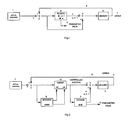
- the block scheme illustrated in Figure 1 refers to a circuit including an actual counting stage 1, an adder 2 in which the sum is formed between the output count from the counting stage 1 and an error 7, a decision stage 3, an adder 4, in which the difference is formed between the sum produced by the adder 2 and the transmitted value 6, and a memory 5 for storing the error 7, which is fed back to the adder 2 by means of a loop 8.
- the remote terminal can reconstruct, on the average, the video synchronisation frequency (clock signal). This is possible due to the integration of the error caused by the jitter and due to the suppression of the latter.
- the counter measuring the video synchronisation frequency does not perform a counting from 0 up to n or n+1; instead, it is preferred for simplifying the circuitry, to use a 5-bit counter that is saturated many times in one period of Fsr.
- a counter that counts the number of transitions of the video synchronisation frequency (clock signal) within a predetermined interval, which may be specifically the frame period of the multiplexer.
- the number of transitions may be 7, 8 or 9; in any other case, an alarm will be caused.
- the latter information that requires 2 bits for being transmitted, is protected by transmitting a suitable 6-bit code (e.g. 13 in Figure 3d); in receiving this code, the information is recovered by a 2/3 majority decision.
- a suitable 6-bit code e.g. 13 in Figure 3d
- FIGS. 3a to 3e together show a detailed circuit structure of this particular embodiment.
- This circuit includes a measuring counter 1 with 5 bits C0, C1, C2, C3 and C4, a counter 11 with 4 bits CF0, CF1, CF2 and CF3 for counting the transitions of the video synchronisation frequency FSINC within the frame period, and a circuit 12 which detects the transitions (leading slopes) of FSINC.
- Figure 3b specifically shows the circuit that carries out the real algorithm and which includes the adder 2 for forming an algebraic sum (using a representation of negative numbers in two's complement) of the count from the counter 1 and the error 7 - ES, ER(4), ER(3), ER(2), ER(1) and ER(0) -, followed by the limiter 10 which is controlled by the underflow and overflow signals UD and OV.
- the limiter 10 Connected to the limiter 10 is an adder 4 for adding the controlled sum and the transmitted data D (0), the output of the adder 4 forming the future error.
- a logic circuit 16 necessary for encoding the number of transitions of FSINC within the frame period and for preparing the 16 bits SYPA (15 : 0) to be sent within the frame, completes this embodiment.
Landscapes
- Engineering & Computer Science (AREA)
- Multimedia (AREA)
- Signal Processing (AREA)
- Compression Or Coding Systems Of Tv Signals (AREA)
- Synchronisation In Digital Transmission Systems (AREA)
Claims (7)
- Verfahren zum Verarbeiten und Übertragen eines durch Synchronisationsstörung beeinträchtigten Taktsignals, wobei die Periode 1/Fsr des Taktsignals mit einem Probensignal der Frequenz Fc gemessen wird, umfassend die folgenden Schritte:
es wird eine diskrete binäre Messung (1) des Verhältnisses Fc/Fsr vorgenommen;
das gemessene Verhältnis Fc/Fsr wird verarbeitet, um die Synchronisationsstörung mittels einer Schaltung (2, 4, 5, 8) zu komprimieren und entfernen, wobei die Schaltung eine Rückkopplungsschleife (8) aufweist, die einen durch die Synchronisationsstörung eingeleiteten Fehler (7) rückkoppelt und dadurch den Fehler akkumuliert und integriert; und
aufgrund der Summe aus dem gemessenen Verhältnis Fc/Fsr und dem Fehler wird eine jeweils die Periode des Taktsignals angebende einzelne Binärziffer ("0" oder "1") erzeugt. - Verfahren nach Anspruch 1, wobei eine binäre "0" erzeugt wird, wenn die Summe aus dem gemessenen Verhältnis Fc/Fsr und dem Fehler ≦ n (n: ganze Zahl) ist, und eine binäre "1" erzeugt wird, wenn die besagte Summe ≧ n + 1 ist, oder umgekehrt.
- Schaltung zur Verarbeitung und Übertragung eines durch Synchronisationsstörung beeinträchtigten Taktsignals, wobei die Periode 1/Fsr des Taktsignals mit einem Probensignal der Frequenz Fc gemessen wird, umfassend
eine Einrichtung (1) zur Durchführung einer diskreten binären Messung des Verhältnisses Fc/Fsr,
eine Einrichtung (2, 4, 5, 8) zur Anwendung eines Algorithmus auf das Verhältnis Fc/Fsr zur Unterdrückung und Entfernung der Synchronisationsstörung, wobei die Einrichtung eine Rückkopplungsschleife (8) aufweist, um einen durch die Synchronisationsstörung eingeleiteten Fehler (7) rückzukoppeln und dadurch den Fehler zu akkumulieren und integrieren, und
eine Einrichtung (3) zur Erzeugung einer jeweils die Periode des Taktsignals angebenden einzelnen Binärziffer ("0" oder "1") aufgrund der Summe aus dem gemessenen Verhältnis Fc/Fsr und dem Fehler (7). - Schaltung nach Anspruch 3 mit einem Sättigungszähler zur Messung der Periode 1/Fsr des Taktsignals.
- Schaltung nach Anspruch 4 mit einem Zähler, der die Anzahl von Durchgängen des Sättigungszählers zählt und somit das Verhältnis Fc/Fsr entsprechend der Anzahl der Durchgänge des Taktsignals innerhalb eines vorgegebenen Zeitintervals bestimmt.
- Schaltung nach Anspruch 4 oder 5, wobei die Einrichtung zur Anwendung des Algorithmus einen Addierer (2) umfaßt, der eine algebraische Summe aus dem der Periode 1/Fsr des Taktsignals entsprechenden Ausgang des Sättigungszählers und dem akkumulierten und integrierten Synchronisationsstörungs-Fehler bildet.
- Schaltung nach Anspruch 6, ferner umfassend eine Alarmeinrichtung zur Anzeige einer Unterschreitung oder eines Überlaufs des Zählers (2).
Applications Claiming Priority (2)
| Application Number | Priority Date | Filing Date | Title |
|---|---|---|---|
| IT2095288 | 1988-06-14 | ||
| IT20952/88A IT1219709B (it) | 1988-06-14 | 1988-06-14 | Sistema e circuiti per l'elaborazione e la trasmissione di un segnale di orologio,in particolare della frequenza di sincronismo video |
Publications (2)
| Publication Number | Publication Date |
|---|---|
| EP0346856A1 EP0346856A1 (de) | 1989-12-20 |
| EP0346856B1 true EP0346856B1 (de) | 1993-02-24 |
Family
ID=11174543
Family Applications (1)
| Application Number | Title | Priority Date | Filing Date |
|---|---|---|---|
| EP89110730A Expired - Lifetime EP0346856B1 (de) | 1988-06-14 | 1989-06-13 | Verfahren und Schaltung zur Verarbeitung und Übertragung eines Taktsignals, speziell der Videosynchronisationsfrequenz |
Country Status (4)
| Country | Link |
|---|---|
| US (1) | US5025460A (de) |
| EP (1) | EP0346856B1 (de) |
| DE (1) | DE68904990T2 (de) |
| IT (1) | IT1219709B (de) |
Families Citing this family (2)
| Publication number | Priority date | Publication date | Assignee | Title |
|---|---|---|---|---|
| BE1003827A4 (fr) * | 1990-02-26 | 1992-06-23 | Alcatel Bell Sdt Sa | Procede universel de codage de signaux d'image. |
| JP3327397B2 (ja) * | 1991-03-12 | 2002-09-24 | ソニー株式会社 | 偏向補正波形発生回路 |
Family Cites Families (11)
| Publication number | Priority date | Publication date | Assignee | Title |
|---|---|---|---|---|
| US3530238A (en) * | 1967-12-04 | 1970-09-22 | Gen Telephone & Elect | Digital synchronizing system for television receivers |
| GB1580060A (en) * | 1976-09-01 | 1980-11-26 | Racal Res Ltd | Electrical circuit arrangements |
| US4740998A (en) * | 1981-03-30 | 1988-04-26 | Data General Corporation | Clock recovery circuit and method |
| US4466111A (en) * | 1981-11-27 | 1984-08-14 | Gte Products Corporation | Synchronization apparatus and method |
| IT1155558B (it) * | 1982-07-19 | 1987-01-28 | Cselt Centro Studi Lab Telecom | Procedimento e strumento per la misura dell ampiezza di un segnale periodico fortemente affetto da rumore e senza riferimento di fase |
| GB2140239B (en) * | 1983-05-18 | 1986-10-08 | Sony Corp | Television frame signal synchronizing circuits |
| JPS6098770A (ja) * | 1983-11-04 | 1985-06-01 | Funai Denki Kk | 同期回路 |
| EP0271218B1 (de) * | 1986-11-11 | 1994-06-29 | Matsushita Electric Industrial Co., Ltd. | Bitsynchronisierungseinstellung in einer Daten-Sende/Empfangsanlage |
| US4769760A (en) * | 1987-03-13 | 1988-09-06 | Cherne Medical, Inc. | Terrain biased dynamic multiple threshold synchronization method and apparatus |
| US4815109A (en) * | 1987-06-25 | 1989-03-21 | Racal Data Communications Inc. | Sampling clock synchronization |
| US4796280A (en) * | 1987-11-06 | 1989-01-03 | Standard Microsystems Corporation | Digital data separator |
-
1988
- 1988-06-14 IT IT20952/88A patent/IT1219709B/it active
-
1989
- 1989-06-13 EP EP89110730A patent/EP0346856B1/de not_active Expired - Lifetime
- 1989-06-13 DE DE8989110730T patent/DE68904990T2/de not_active Expired - Lifetime
- 1989-06-14 US US07/365,846 patent/US5025460A/en not_active Expired - Lifetime
Also Published As
| Publication number | Publication date |
|---|---|
| EP0346856A1 (de) | 1989-12-20 |
| IT1219709B (it) | 1990-05-24 |
| DE68904990T2 (de) | 1993-09-02 |
| DE68904990D1 (de) | 1993-04-01 |
| US5025460A (en) | 1991-06-18 |
| IT8820952A0 (it) | 1988-06-14 |
Similar Documents
| Publication | Publication Date | Title |
|---|---|---|
| EP0540177B1 (de) | Nachrichtenübertragungsverfahren und -vorrichtung | |
| JP2670259B2 (ja) | 高能率符号化装置 | |
| US4387460A (en) | Supplementary information transmitting arrangement for a digital data transmission system | |
| DE69128057T2 (de) | Erkennungsgerät für Bitfehlerrate | |
| EP0627859A2 (de) | Hierarchische Kodierung und/oder Dekodierung von digitalen Bildsignalen | |
| EP1513306A3 (de) | Schnittstellenschaltung zur Ersetzung von Nullwörtern für Telekommunikationsgeräte | |
| US4411001A (en) | Differential pulse code modulation transmission system | |
| US5574752A (en) | Moving image data transmitter and receiver frame synchronization | |
| US4622579A (en) | Method and apparatus for transmitting digital luminance and chrominance television signals | |
| EP0555215B1 (de) | Mehrkanaliger datenkompressor | |
| US5418573A (en) | Apparatus and method for producing periodic synchronization references forming a synchronization signal | |
| EP0498081B1 (de) | Videokodierer und -dekodierer mit Verschiebungsverhinderung für korrekt dekodierte Signalblöcke | |
| US4791485A (en) | System for detecting a transmission error | |
| HK1040336A1 (en) | Audio coder utilising repeated transmission of packet portion | |
| EP0346856A1 (de) | Verfahren und Schaltung zur Verarbeitung und Übertragung eines Taktsignals, speziell der Videosynchronisationsfrequenz | |
| US3568063A (en) | Sliding scale predictive coding system | |
| CA2005194C (en) | Synchronizing circuit for reducing waiting-time jitter in a demultiplexer | |
| JPS62272632A (ja) | テレビ信号の分割伝送装置 | |
| US4477915A (en) | Differential pulse code modulation transmission system | |
| US4297744A (en) | Process and device for multiplying a stochastic value by a coefficient greater than the unit | |
| US6023294A (en) | Bit budget estimation method and device for variable word length encoders | |
| JP2868646B2 (ja) | 画像信号符号化装置 | |
| Thompson | A 36-Mbit/s television codec employing pseudorandom quantization | |
| Ibrahim et al. | Six-bit DPCM video signal processing and implementation using systolic arrays | |
| KR0169396B1 (ko) | 갈로아 필드 곱셈기를 이용한 리드-솔로몬 디코더 |
Legal Events
| Date | Code | Title | Description |
|---|---|---|---|
| PUAI | Public reference made under article 153(3) epc to a published international application that has entered the european phase |
Free format text: ORIGINAL CODE: 0009012 |
|
| AK | Designated contracting states |
Kind code of ref document: A1 Designated state(s): BE CH DE ES FR GB GR LI NL SE |
|
| 17P | Request for examination filed |
Effective date: 19900615 |
|
| 17Q | First examination report despatched |
Effective date: 19901218 |
|
| RTI1 | Title (correction) | ||
| GRAA | (expected) grant |
Free format text: ORIGINAL CODE: 0009210 |
|
| RAP1 | Party data changed (applicant data changed or rights of an application transferred) |
Owner name: ALCATEL ITALIA SOCIETA PER AZIONI |
|
| AK | Designated contracting states |
Kind code of ref document: B1 Designated state(s): BE CH DE ES FR GB GR LI NL SE |
|
| PG25 | Lapsed in a contracting state [announced via postgrant information from national office to epo] |
Ref country code: LI Effective date: 19930224 Ref country code: NL Effective date: 19930224 Ref country code: CH Effective date: 19930224 Ref country code: SE Effective date: 19930224 Ref country code: ES Free format text: THE PATENT HAS BEEN ANNULLED BY A DECISION OF A NATIONAL AUTHORITY Effective date: 19930224 Ref country code: GR Free format text: LAPSE BECAUSE OF FAILURE TO SUBMIT A TRANSLATION OF THE DESCRIPTION OR TO PAY THE FEE WITHIN THE PRESCRIBED TIME-LIMIT Effective date: 19930224 Ref country code: BE Effective date: 19930224 |
|
| REF | Corresponds to: |
Ref document number: 68904990 Country of ref document: DE Date of ref document: 19930401 |
|
| ET | Fr: translation filed | ||
| REG | Reference to a national code |
Ref country code: CH Ref legal event code: PL |
|
| NLV1 | Nl: lapsed or annulled due to failure to fulfill the requirements of art. 29p and 29m of the patents act | ||
| PLBE | No opposition filed within time limit |
Free format text: ORIGINAL CODE: 0009261 |
|
| STAA | Information on the status of an ep patent application or granted ep patent |
Free format text: STATUS: NO OPPOSITION FILED WITHIN TIME LIMIT |
|
| 26N | No opposition filed | ||
| REG | Reference to a national code |
Ref country code: GB Ref legal event code: IF02 |
|
| PGFP | Annual fee paid to national office [announced via postgrant information from national office to epo] |
Ref country code: DE Payment date: 20080620 Year of fee payment: 20 |
|
| PGFP | Annual fee paid to national office [announced via postgrant information from national office to epo] |
Ref country code: FR Payment date: 20080613 Year of fee payment: 20 |
|
| PGFP | Annual fee paid to national office [announced via postgrant information from national office to epo] |
Ref country code: GB Payment date: 20080620 Year of fee payment: 20 |
|
| REG | Reference to a national code |
Ref country code: GB Ref legal event code: PE20 Expiry date: 20090612 |
|
| PG25 | Lapsed in a contracting state [announced via postgrant information from national office to epo] |
Ref country code: GB Free format text: LAPSE BECAUSE OF EXPIRATION OF PROTECTION Effective date: 20090612 |