EP0343345A1 - Filter in Streifenleiter-Technik - Google Patents
Filter in Streifenleiter-Technik Download PDFInfo
- Publication number
- EP0343345A1 EP0343345A1 EP89105491A EP89105491A EP0343345A1 EP 0343345 A1 EP0343345 A1 EP 0343345A1 EP 89105491 A EP89105491 A EP 89105491A EP 89105491 A EP89105491 A EP 89105491A EP 0343345 A1 EP0343345 A1 EP 0343345A1
- Authority
- EP
- European Patent Office
- Prior art keywords
- filter
- resonator
- conductor
- frequency
- filter device
- Prior art date
- Legal status (The legal status is an assumption and is not a legal conclusion. Google has not performed a legal analysis and makes no representation as to the accuracy of the status listed.)
- Granted
Links
- 239000004020 conductor Substances 0.000 claims abstract description 85
- 239000000758 substrate Substances 0.000 claims abstract description 43
- 230000004044 response Effects 0.000 claims abstract description 16
- 230000000875 corresponding effect Effects 0.000 abstract 1
- 230000005540 biological transmission Effects 0.000 description 3
- 230000002093 peripheral effect Effects 0.000 description 3
- 230000004075 alteration Effects 0.000 description 2
- 230000008901 benefit Effects 0.000 description 2
- 230000004048 modification Effects 0.000 description 2
- 238000012986 modification Methods 0.000 description 2
- 239000003990 capacitor Substances 0.000 description 1
- 230000008859 change Effects 0.000 description 1
- 238000005520 cutting process Methods 0.000 description 1
- 239000003989 dielectric material Substances 0.000 description 1
- 239000006185 dispersion Substances 0.000 description 1
- 238000003754 machining Methods 0.000 description 1
- 238000004519 manufacturing process Methods 0.000 description 1
- 239000002184 metal Substances 0.000 description 1
- 238000005488 sandblasting Methods 0.000 description 1
Images


Classifications
-
- H—ELECTRICITY
- H01—ELECTRIC ELEMENTS
- H01P—WAVEGUIDES; RESONATORS, LINES, OR OTHER DEVICES OF THE WAVEGUIDE TYPE
- H01P1/00—Auxiliary devices
- H01P1/20—Frequency-selective devices, e.g. filters
- H01P1/201—Filters for transverse electromagnetic waves
- H01P1/203—Strip line filters
- H01P1/20327—Electromagnetic interstage coupling
- H01P1/20336—Comb or interdigital filters
Definitions
- the present invention relates to a filter device of a three-conductor structure type adapted for use miniature electronic circuits.
- a filter device of a three-conductor structure type in which a stripline pattern is disposed between contact surfaces of two dielectric substrates stacked and comprises a plurality of juxtaposed resonator conductors.
- Such a filter device is of small size and simple, and thus is preferably used in the miniature electronic circuits.
- the conventional filter device of a three-conductor structure type has a frequency response which depends on the size of the resonator conductors, the structure of an external conductor to which the resonator conductors are connected, the configuration and dielectric constant of the substrates or other factors. Therefore, if there are any dispersions in the configuration and dielectric constant of the substrates or the like, the frequency response of the filter may substantially be varied so that it may be deviated from a predetermined frequency range.
- the dielectric substrate comes into direct contact with the casing via the removed portion of the external conductor or an opening.
- the distributed capacity may be varied so that the frequency may be deviated.
- Another object of the present invention is to provide a filter device which fully meets with the requirement for smaller and thinner dimensions of the miniature electronic circuits.
- a three-conductor type filter comprising two dielectric substrates which are stacked to each other, a stripline pattern resonator including a plurality of juxtaposed resonator conductors and disposed on the surface of one of said dielectric substrates which is brought into contact with the other dielectric substrate, outer conductor layers each formed on each of said dielectric substrates so that it surrounds the outer surface and side portion of said each dielectric substrate, said outer conductor layer formed on said one dielectric substrate being connected to one ends of said juxtaposed resonator conductors, and openings each provided on the lateral portions of said outer conductor layers corresponding to said one end of the each resonator conductor for lowering the frequency of response of the filter.
- Each opening may be provided with a removable conductor strip for increasing the frequency of response of the filter.
- the center frequency of the filter is shifted toward the higher frequency side, said opening(s) is formed to reduce the frequency.
- a conductor stripe is applied to the formed opening(s) to shift the center frequency toward the higher frequency side.
- the frequency adjusting openings are provided on the side portions of the filter body, so that the outer surfaces of the filter body can be brought into contact with the inner surfaces of a casing without making any trouble.
- a suitable space may be maintained between the each opening and the opposite lateral wall of the casing without causing the total thickness or height of the filter to increase.
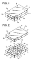
- Figs. 1 and 2 illustrate a filter of a three-conductor structure type according to an embodiment of the present invention.
- the illustrated filter comprises a lower and upper dielectric substrates 1 and 2 which are to be stacked to each other upon the assembling of the filter.
- the lower dielectric substrate 1 has one surface provided with a stripline pattern resonator 3 which includes three resonator conductors 4, 5 and 6 juxtapositionally interdigitated.
- Each of the resonator conductors 4, 5 and 6 has a length set to substantially one quarter of the wavelength of an intended resonance frequency of the resonator 3.
- An outer conductor layer 7 is provided on the other surface and peripheral portion of the lower dielectric substrate 1, and is extended about the edge portion of the one surface thereof so as to substantially surround the juxtapositionally interdigitated resonator conductors 4, 5 and 6. As shown in Fig.
- the outer conductor layer 7 is integrally connected to the one end of each of the resonator conductors 4, 5 and 6.
- the other end or open circuit end of each resonator conductor is spaced from the associated edge portion 7a or 7b of the outer conductor layer 7.
- the outer conductor layer 7 has notches 7c and 7d for forming clearances for lateral extensions 4a and 5a of the outer conductor layer 4 and 5, respectively,
- One of the extensions 4a and 5a is formed as a signal input electrode and the other extension is formed as a signal output electrode.
- the upper dielectric substrate 2 to be stacked onto the lower dielectric substrate 1 is provided with an outer conductor layer 8 on the upper surface and peripheral portion thereof.
- the outer conductor layer 8 is electrically connected to the outer conductor layer 7 of the lower dielectric substrate 1 when being assembled.
- the upper dielectric substrate 2 has grooves 2a and 2b which are positioned corresponding to the lateral extensions 4a and 5a on the lower dielectric substrate 1. These grooves 2a and 2b may be provided to be accessible when the signal input and output electrodes 4a and 5a or 5a and 4a are connected to an input and output conductors connected with a circuit board, not shown.
- the outer conductor layers 7 and 8 on the lower and upper dielectric substrates 1 and 2 are provided with notches 10 and 11 at regions corresponding to the one ends of the respective resonator conductors 4, 5 and 6, respectively. These notches 10 and 11 form rectangular openings 12 for adjusting the frequency response of the filter when the lower and upper dielectric substrates 1 and 2 are assembled.
- the notches 10 and 11 may be formed by printing the outer conductor layers 7 and 8 on the lower and upper dielectric substrates 1 and 2, respectively, excepting said regions, or removing the outer conductor layers 7 and 8 at said regions by means of a cutting tool, a laser beam machining, a sand blasting or the like.
- the casing 13 may be formed of metal, and has an inner height equal to the height of the filter and a width larger than that of the filter.
- the center of the response frequency thereof is adjusted toward a lower direction. Therefore, if the center frequency of the filter is higher than an intended reference level, the correction can be performed by providing the openings 12. On the other hand, if the center frequency is lower that the intended reference level, the correction can be performed by applying a conductor strip to each opening 12.
- the conductor strip may previously be applied to each opening 12 upon the manufacturing of the filter. In this case, the response frequency of the filter is corrected by peeling off the conductor strip applied to the each opening 12.
- the resonator conductors 4, 5 and 6 may be arranged in a comb shape to be extended from the same edge portion 7a or 7b of the outer conductor layer 7.
- the upper dielectric substrate 2 may be provided with a transmission line pattern on the lower surface, which is disposed to have a reflected image relation with respect to the stripline pattern 3 on the lower dielectric substrate 1.
- the inner side walls may be brought into contact with the lateral surfaces of the filter including the adjusting openings.
- the inner length of the casing 13 is determined to be equal to the length of the filter so that both inner end walls (only one of which is represented by 13a in Fig. 5) of the casing 13 come into contact with the end surfaces (only one of which is represented by 14 in Fig. 5) of the filter.
- Each of the inner end walls is outwards protruded at region(s) opposite to the opening(s) 12 so as to form inner recess(es) 15, thereby preventing the portions of the dielectric substrates 1 and 2 exposed through each opening 12 from bring into contact with the associated inner end surface of the casing 13.
- Fig. 6 shows a further embodiment in which rectangular recesses 16 are provided on the portions of the dielectric substrates 1 and 2 which are opposite to the respective openings 12.
- the portions of the dielectric substrates 1 and 2 exposed through each opening 12 can be prevented from bring into contact with the associated inner end surface of the casing 13 when the filter is inserted into the casing 13 so that the inner end surfaces 13a abut the outer conductor layers 7 and 8.
- Figs. 7, 8 and 9 show respectively the transmission and reflection characteristics (a) and (b) of the filter.
- Fig. 7 shows the case that the center frequency f1 of the filter is shifted to the low frequency side of a desired center frequency f0.
- the deviation of the center frequency f1 of the filter can be corrected so that the center frequency f1 corresponds to the desired center frequency f0 as shown in Fig. 9.
- the filter device of the present invention has an advantage that there is no variation or deviation in the set frequency characteristic of the filter when the filter device is completed by inserting the filter into the casing. Further the present invention has also an advantage that a frequency adjustment can be easily and correctly made without substantially increasing the thickness or height of the casing, thus contributing to miniaturization of a filter circuit apparatus.
Landscapes
- Physics & Mathematics (AREA)
- Electromagnetism (AREA)
- Control Of Motors That Do Not Use Commutators (AREA)
Applications Claiming Priority (2)
| Application Number | Priority Date | Filing Date | Title |
|---|---|---|---|
| JP79981/88 | 1988-03-30 | ||
| JP63079981A JPH01251801A (ja) | 1988-03-30 | 1988-03-30 | 三導体構造フィルタ |
Publications (2)
| Publication Number | Publication Date |
|---|---|
| EP0343345A1 true EP0343345A1 (de) | 1989-11-29 |
| EP0343345B1 EP0343345B1 (de) | 1993-06-02 |
Family
ID=13705500
Family Applications (1)
| Application Number | Title | Priority Date | Filing Date |
|---|---|---|---|
| EP89105491A Expired - Lifetime EP0343345B1 (de) | 1988-03-30 | 1989-03-28 | Filter in Streifenleiter-Technik |
Country Status (4)
| Country | Link |
|---|---|
| US (1) | US4975664A (de) |
| EP (1) | EP0343345B1 (de) |
| JP (1) | JPH01251801A (de) |
| DE (1) | DE68906823T2 (de) |
Cited By (5)
| Publication number | Priority date | Publication date | Assignee | Title |
|---|---|---|---|---|
| EP0396480A1 (de) * | 1989-05-03 | 1990-11-07 | NGK Spark Plug Co. Ltd. | Verfahren zum Einstellen des Frequenzganges einer Filtereinrichtung vom Dreileiter-Typ |
| GB2240432A (en) * | 1990-01-08 | 1991-07-31 | Ngk Spark Plug Co | Stripline filter |
| DE4024146A1 (de) * | 1990-07-30 | 1992-02-13 | Telefunken Electronic Gmbh | Hf-filter |
| EP0437304A3 (en) * | 1990-01-12 | 1992-05-06 | Ngk Spark Plug Co. Ltd. | Method of adjusting a frequency response in a stripline filter device |
| EP3093916A1 (de) * | 2015-05-15 | 2016-11-16 | Innertron, Inc. | Resonanzvorrichtung und filter damit |
Families Citing this family (12)
| Publication number | Priority date | Publication date | Assignee | Title |
|---|---|---|---|---|
| JPH0334305U (de) * | 1989-08-14 | 1991-04-04 | ||
| KR0174531B1 (ko) * | 1989-11-20 | 1999-04-01 | 이우에 사또시 | 마이크로 스트립 라인을 이용한 대역 필터 및 필터 특성 조정 방법 |
| US5293140A (en) * | 1991-01-02 | 1994-03-08 | Motorola, Inc. | Transmission line structure |
| EP0506476B1 (de) * | 1991-03-29 | 1996-06-05 | Ngk Insulators, Ltd. | Dielektrische Filter mit Koppelelektroden um Resonatoren oder Elektroden zu Verbinden, und Verfahren zur Einstellung der Frequenzcharakteristik des Filters |
| US5412358A (en) * | 1992-02-28 | 1995-05-02 | Ngk Insulators, Ltd. | Layered stripline filter |
| US5379012A (en) * | 1992-04-30 | 1995-01-03 | Ngk Spark Plug Co., Ltd. | Dielectric filter device |
| KR0148749B1 (ko) * | 1992-10-14 | 1998-08-17 | 모리시다 요오이찌 | 필터 및 그 제조방법 |
| JPH06314915A (ja) * | 1993-04-30 | 1994-11-08 | Tokin Corp | 誘電体共振器及びその共振周波数調整方法 |
| US5416454A (en) * | 1994-03-31 | 1995-05-16 | Motorola, Inc. | Stripline filter with a high side transmission zero |
| US5770987A (en) * | 1996-09-06 | 1998-06-23 | Henderson; Bert C. | Coplanar waVeguide strip band pass filter |
| JP2002043881A (ja) * | 2000-07-31 | 2002-02-08 | Murata Mfg Co Ltd | 積層型lcフィルタおよびその周波数調整方法 |
| JP4046564B2 (ja) * | 2002-07-12 | 2008-02-13 | 三菱電機株式会社 | 光半導体装置 |
Citations (4)
| Publication number | Priority date | Publication date | Assignee | Title |
|---|---|---|---|---|
| US4157517A (en) * | 1977-12-19 | 1979-06-05 | Motorola, Inc. | Adjustable transmission line filter and method of constructing same |
| WO1981001079A1 (en) * | 1979-10-15 | 1981-04-16 | Motorola Inc | Thin film structure for ceramic substrates |
| EP0093956A2 (de) * | 1982-05-10 | 1983-11-16 | Oki Electric Industry Company, Limited | Dielektrisches Filter |
| WO1985000929A1 (en) * | 1983-08-15 | 1985-02-28 | American Telephone & Telegraph Company | Microwave circuit device and its fabrication |
Family Cites Families (7)
| Publication number | Priority date | Publication date | Assignee | Title |
|---|---|---|---|---|
| JPS5362904A (en) * | 1976-11-17 | 1978-06-05 | Fujitsu Ltd | Bothway collision control system for bothway circuit |
| US4266206A (en) * | 1978-08-31 | 1981-05-05 | Motorola, Inc. | Stripline filter device |
| JPS58204602A (ja) * | 1982-05-24 | 1983-11-29 | Murata Mfg Co Ltd | 誘電体同軸共振器の共振周波数調整方法 |
| JPS62263702A (ja) * | 1986-05-09 | 1987-11-16 | Murata Mfg Co Ltd | ストリツプラインフイルタ |
| JPS62104201A (ja) * | 1985-10-30 | 1987-05-14 | Fujitsu Ltd | 誘電体フイルタ |
| US4785271A (en) * | 1987-11-24 | 1988-11-15 | Motorola, Inc. | Stripline filter with improved resonator structure |
| US4837534A (en) * | 1988-01-29 | 1989-06-06 | Motorola, Inc. | Ceramic block filter with bidirectional tuning |
-
1988
- 1988-03-30 JP JP63079981A patent/JPH01251801A/ja active Pending
-
1989
- 1989-03-27 US US07/329,312 patent/US4975664A/en not_active Expired - Lifetime
- 1989-03-28 DE DE8989105491T patent/DE68906823T2/de not_active Expired - Fee Related
- 1989-03-28 EP EP89105491A patent/EP0343345B1/de not_active Expired - Lifetime
Patent Citations (4)
| Publication number | Priority date | Publication date | Assignee | Title |
|---|---|---|---|---|
| US4157517A (en) * | 1977-12-19 | 1979-06-05 | Motorola, Inc. | Adjustable transmission line filter and method of constructing same |
| WO1981001079A1 (en) * | 1979-10-15 | 1981-04-16 | Motorola Inc | Thin film structure for ceramic substrates |
| EP0093956A2 (de) * | 1982-05-10 | 1983-11-16 | Oki Electric Industry Company, Limited | Dielektrisches Filter |
| WO1985000929A1 (en) * | 1983-08-15 | 1985-02-28 | American Telephone & Telegraph Company | Microwave circuit device and its fabrication |
Non-Patent Citations (2)
| Title |
|---|
| PATENT ABSTRACTS OF JAPAN, vol. 6, no. 182 (E-131)[1060], 18th September 1982; & JP-A-57 97 203 (TOKYO SHIBAURA DENKI K.K.) 16-06-1982 * |
| TOUTE L'ELECTRONIQUE, no. 452, March 1980, pages 39-43; J. GOUREVITCH: "Filtres passe-bande extra-plats THF" * |
Cited By (7)
| Publication number | Priority date | Publication date | Assignee | Title |
|---|---|---|---|---|
| EP0396480A1 (de) * | 1989-05-03 | 1990-11-07 | NGK Spark Plug Co. Ltd. | Verfahren zum Einstellen des Frequenzganges einer Filtereinrichtung vom Dreileiter-Typ |
| GB2240432A (en) * | 1990-01-08 | 1991-07-31 | Ngk Spark Plug Co | Stripline filter |
| GB2240432B (en) * | 1990-01-08 | 1994-07-27 | Ngk Spark Plug Co | Stripline filter |
| EP0437304A3 (en) * | 1990-01-12 | 1992-05-06 | Ngk Spark Plug Co. Ltd. | Method of adjusting a frequency response in a stripline filter device |
| DE4024146A1 (de) * | 1990-07-30 | 1992-02-13 | Telefunken Electronic Gmbh | Hf-filter |
| EP3093916A1 (de) * | 2015-05-15 | 2016-11-16 | Innertron, Inc. | Resonanzvorrichtung und filter damit |
| US9627731B2 (en) | 2015-05-15 | 2017-04-18 | Innertron, Inc. | Resonance device and filter including the same |
Also Published As
| Publication number | Publication date |
|---|---|
| JPH01251801A (ja) | 1989-10-06 |
| DE68906823D1 (de) | 1993-07-08 |
| DE68906823T2 (de) | 1993-09-09 |
| EP0343345B1 (de) | 1993-06-02 |
| US4975664A (en) | 1990-12-04 |
Similar Documents
| Publication | Publication Date | Title |
|---|---|---|
| EP0343345B1 (de) | Filter in Streifenleiter-Technik | |
| EP0396480B1 (de) | Verfahren zum Einstellen des Frequenzganges einer Filtereinrichtung vom Dreileiter-Typ | |
| US6014067A (en) | Dielectric resonator filter having a portion of the outer surface closer to the resonators | |
| EP1439599B1 (de) | Dielektrisches Filter vom Hohlleitertyp | |
| EP0499643B1 (de) | Bandpassfilter | |
| EP0069785B1 (de) | Filter mit halben koaxialen hohlraumresonatoren | |
| EP0414619B1 (de) | Verfahren zum Einstellen eines Frequenzganges einer Dreileiter-Filteranordnung | |
| EP0617476A1 (de) | Filter und verfahren zu seiner herstellung | |
| EP0590612B1 (de) | Frequenzabstimmbarer Resonator mit einem Varaktor | |
| EP0635897B1 (de) | Dielektrisches Filter | |
| US5291162A (en) | Method of adjusting frequency response in a microwave strip-line filter device | |
| EP0837519A1 (de) | Dielektrisches Filter | |
| US5304966A (en) | Method of adjusting a frequency response in a three-conductor type filter device | |
| EP0532770B1 (de) | Streifenleitungsfilter für mikrowellen | |
| US5859575A (en) | Dielectric filter | |
| JPH06216605A (ja) | ストリップラインフィルタ | |
| EP0838875B1 (de) | Dielektrisches Filter | |
| JPH0633683Y2 (ja) | 三導体構造フィルタパッケージ | |
| JP2762331B2 (ja) | 誘電体フィルタ | |
| JP2666102B2 (ja) | 積層型誘電体フィルタ | |
| JP2661004B2 (ja) | 誘電体フィルタ | |
| JP2732150B2 (ja) | 誘電体帯域阻止フィルタ | |
| EP0837518B1 (de) | Dielektrisches Filter | |
| JPH06112703A (ja) | 誘電体フィルタ | |
| JP2666101B2 (ja) | 積層型誘電体フィルタ |
Legal Events
| Date | Code | Title | Description |
|---|---|---|---|
| PUAI | Public reference made under article 153(3) epc to a published international application that has entered the european phase |
Free format text: ORIGINAL CODE: 0009012 |
|
| AK | Designated contracting states |
Kind code of ref document: A1 Designated state(s): DE FR GB NL |
|
| 17P | Request for examination filed |
Effective date: 19900321 |
|
| 17Q | First examination report despatched |
Effective date: 19920619 |
|
| GRAA | (expected) grant |
Free format text: ORIGINAL CODE: 0009210 |
|
| AK | Designated contracting states |
Kind code of ref document: B1 Designated state(s): DE FR GB NL |
|
| REF | Corresponds to: |
Ref document number: 68906823 Country of ref document: DE Date of ref document: 19930708 |
|
| ET | Fr: translation filed | ||
| PLBE | No opposition filed within time limit |
Free format text: ORIGINAL CODE: 0009261 |
|
| STAA | Information on the status of an ep patent application or granted ep patent |
Free format text: STATUS: NO OPPOSITION FILED WITHIN TIME LIMIT |
|
| 26N | No opposition filed | ||
| REG | Reference to a national code |
Ref country code: GB Ref legal event code: IF02 |
|
| PGFP | Annual fee paid to national office [announced via postgrant information from national office to epo] |
Ref country code: NL Payment date: 20050303 Year of fee payment: 17 |
|
| PGFP | Annual fee paid to national office [announced via postgrant information from national office to epo] |
Ref country code: FR Payment date: 20050308 Year of fee payment: 17 |
|
| PGFP | Annual fee paid to national office [announced via postgrant information from national office to epo] |
Ref country code: GB Payment date: 20050323 Year of fee payment: 17 |
|
| PGFP | Annual fee paid to national office [announced via postgrant information from national office to epo] |
Ref country code: DE Payment date: 20050324 Year of fee payment: 17 |
|
| PG25 | Lapsed in a contracting state [announced via postgrant information from national office to epo] |
Ref country code: GB Free format text: LAPSE BECAUSE OF NON-PAYMENT OF DUE FEES Effective date: 20060328 |
|
| PG25 | Lapsed in a contracting state [announced via postgrant information from national office to epo] |
Ref country code: NL Free format text: LAPSE BECAUSE OF NON-PAYMENT OF DUE FEES Effective date: 20061001 |
|
| PG25 | Lapsed in a contracting state [announced via postgrant information from national office to epo] |
Ref country code: DE Free format text: LAPSE BECAUSE OF NON-PAYMENT OF DUE FEES Effective date: 20061003 |
|
| GBPC | Gb: european patent ceased through non-payment of renewal fee |
Effective date: 20060328 |
|
| NLV4 | Nl: lapsed or anulled due to non-payment of the annual fee |
Effective date: 20061001 |
|
| REG | Reference to a national code |
Ref country code: FR Ref legal event code: ST Effective date: 20061130 |
|
| PG25 | Lapsed in a contracting state [announced via postgrant information from national office to epo] |
Ref country code: FR Free format text: LAPSE BECAUSE OF NON-PAYMENT OF DUE FEES Effective date: 20060331 |