EP0342631B1 - Pufferspeicher, der zur Speicherung von Befehls- und Datenblöcken auf verschiedene Blockgrössen geeignet ist - Google Patents
Pufferspeicher, der zur Speicherung von Befehls- und Datenblöcken auf verschiedene Blockgrössen geeignet ist Download PDFInfo
- Publication number
- EP0342631B1 EP0342631B1 EP89108845A EP89108845A EP0342631B1 EP 0342631 B1 EP0342631 B1 EP 0342631B1 EP 89108845 A EP89108845 A EP 89108845A EP 89108845 A EP89108845 A EP 89108845A EP 0342631 B1 EP0342631 B1 EP 0342631B1
- Authority
- EP
- European Patent Office
- Prior art keywords
- operand
- cache
- instruction
- block
- buffer
- Prior art date
- Legal status (The legal status is an assumption and is not a legal conclusion. Google has not performed a legal analysis and makes no representation as to the accuracy of the status listed.)
- Expired - Lifetime
Links
Images

Classifications
-
- G—PHYSICS
- G06—COMPUTING OR CALCULATING; COUNTING
- G06F—ELECTRIC DIGITAL DATA PROCESSING
- G06F9/00—Arrangements for program control, e.g. control units
- G06F9/06—Arrangements for program control, e.g. control units using stored programs, i.e. using an internal store of processing equipment to receive or retain programs
- G06F9/30—Arrangements for executing machine instructions, e.g. instruction decode
- G06F9/38—Concurrent instruction execution, e.g. pipeline or look ahead
- G06F9/3802—Instruction prefetching
- G06F9/3814—Implementation provisions of instruction buffers, e.g. prefetch buffer; banks
-
- G—PHYSICS
- G06—COMPUTING OR CALCULATING; COUNTING
- G06F—ELECTRIC DIGITAL DATA PROCESSING
- G06F12/00—Accessing, addressing or allocating within memory systems or architectures
- G06F12/02—Addressing or allocation; Relocation
- G06F12/08—Addressing or allocation; Relocation in hierarchically structured memory systems, e.g. virtual memory systems
- G06F12/0802—Addressing of a memory level in which the access to the desired data or data block requires associative addressing means, e.g. caches
- G06F12/0877—Cache access modes
- G06F12/0886—Variable-length word access
-
- G—PHYSICS
- G06—COMPUTING OR CALCULATING; COUNTING
- G06F—ELECTRIC DIGITAL DATA PROCESSING
- G06F9/00—Arrangements for program control, e.g. control units
- G06F9/06—Arrangements for program control, e.g. control units using stored programs, i.e. using an internal store of processing equipment to receive or retain programs
- G06F9/30—Arrangements for executing machine instructions, e.g. instruction decode
- G06F9/38—Concurrent instruction execution, e.g. pipeline or look ahead
- G06F9/3802—Instruction prefetching
Definitions
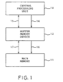
- the write-in request be issued as either the operand fetch request or the instruction fetch request through the request line 14 from the central processing unit 10 to the buffer memory device 12.
- the write-in request is specified by the request signal indicative of either the instruction or the operand fetch request, the flag signal representative of the write-in request, and the memory address signal together with a write-in data signal.
- the memory address is indicative of a write-in address. If the write-in data signal can be memorized in the buffer memory device 12, the write-in data signal is memorized in the buffer memory device 12. Otherwise, data transfer is carried out from the main memory 11 to the buffer memory device 12 through the block data line 17 to memorize a data block corresponding to the write-in address signal. In this event, the write-in data signal is also memorized in the main memory 11.
- the request line 14 is used in common to both the operand and the instruction fetch requests, different lines may be individually used for the operand and the instruction fetch requests.
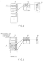
- the AND gate circuit 55 supplies the central processing unit 10 (Fig. 1) as the reply signal with a logic "1" level signal indicative of presence of a required operand data block in the cache memory 22.
- the required operand data block is read out of the first cache address of the data buffer 41 and is transferred through the reply line 15 to the central processing unit 10.
- block data transfer of the instruction data block in question is carried out between the main memory 11 and the buffer memory device 12 through the block data line 17 (Figs. 1 and 2) in the manner mentioned before.
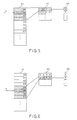
- a leading one of the cache areas for the required instruction data block is kept in the second register 27 of the data processor 21 (Fig. 2).
- the required instruction data block is written into the leading cache area and is thereafter continuously written into three consecutive cache areas following the leading cache area.
- two least significant bits of the address signal kept in the second register 27 may be neglected during such a write-in operation.
- the zeroth cache area is indicated as the leading cache area.
Landscapes
- Engineering & Computer Science (AREA)
- Theoretical Computer Science (AREA)
- Software Systems (AREA)
- Physics & Mathematics (AREA)
- General Engineering & Computer Science (AREA)
- General Physics & Mathematics (AREA)
- Memory System Of A Hierarchy Structure (AREA)
- Advance Control (AREA)
Claims (5)
- Pufferspeicher (12), der zwischen einer Zentraleinheit (10) und einem Hauptspeicher (11) liegt und betriebsbereit ist, um als Antwort auf eine Operandenanforderung und eine Befehlsanforderung, die jeweils von der Zentraleinheit (10) ausgegeben werden, wahlweise einen Operandendatenblock und einen Befehlsdatenblock zu speichern und auszulesen, wobei der Pufferspeicher (12) einen Cachespeicher (22) mit mehreren Cachespeicherbereichen (D0 bis D3) aufweist, von denen jeder eine bestimmte Bereichsgröße besitzt,
dadurch gekennzeichnet,daß der Operandendatenblock eine Operandenblockgröße der bestimmten Bereichsgröße besitzt, während der Befehlsdatenblock eine Befehlsblockgröße besitzt, die gleich N mal der Operandenblockgröße ist, wobei N eine ganze Zahl größer als Eins ist;daß der Pufferspeicher (12) aufweist:eine sowohl auf die Operanden- als auch die Befehlsanforderung ansprechende Erzeugungseinrichtung (21) zum Erzeugen eines Cachespeicherbereichsadressensignals, um als Antwort auf die Operanden- bzw. Befehlsanforderungen auf den Cachespeicher (22) auf der Operandenblockgröße und auf der Befehlsblockgröße zuzugreifen, wobei das Cachespeicherbereichsadressensignal an den Cachespeicher übergeben wird; undeine mit der Erzeugungseinrichtung (21) und dem Cachespeicher (22) verbundene Cachespeicherüberwachungseinrichtung (23) zum Überwachen des Cachespeichers (22) mit Bezug auf das Cachespeicherbereichsadressensignal. - Puffereinrichtung nach Anspruch 1, wobei die Cachespeicherbereiche des Cachespeichers (22) mit den Operanden- und den Befehlsdatenblöcken aufgefüllt werden, wobei die Cachespeicherüberwachungseinrichtung (23) aufweist:eine mit der Erzeugungseinrichtung (21) verbundene Blockinformationsspeichereinrichtung (51) zum Speichern eines Blockinformationssignals, das kennzeichnet, welcher der Operandenund der Befehlsdatenblöcke in jedem der Cachespeicherbereiche gespeichert wird, um als Antwort auf das Cachespeicherbereichsadressensignal ein gespeichertes Blockinformationssignal zu erzeugen; undeine auf das Cachespeicherbereichsadressensignal ansprechende Nachweiseinrichtung zum Nachweisen, ob das gespeicherte Blockinformationssignal den Operanden- oder den Befehlsdatenblock kennzeichnet, um den Cachespeicher (22) zu überwachen.
- Pufferspeicher nach Anspruch 1 oder 2, wobei sowohl die Operanden- als auch die Befehlsanforderung ein Speicheradressensignal aufweist, das aus einem ersten signifikanten Teil und einem, zweiten signifikanten Teil besteht, der als Bereichsadressensignal zum Bestimmen der Cachespeicherbereiche betreibbar ist, wobei der Cachespeicher (22) aufweist:einen Datenpuffer (41), der mehrere Cachespeicherbereiche (D0 bis D3) besitzt und auf die durch das Cachespeicherbereichsadressensignal von der Erzeugungseinrichtung (21) zugegriffen werden kann, wobei der Datenpuffer (41) zum Speichern der Operanden- und der Befehlsdatenblöcke in den Cachespeicherbereichen als gespeicherte Blöcke dient, wobei der Operandendatenblock den einzigen der Cachespeicherbereiche (D0 bis D3) belegt und jeder der Befehlsdatenblöcke mehrere Cachespeicherbereiche belegt;einen Adressenpuffer (42), der mehrere Adressenpufferbereiche (A0 bis A3) besitzt, deren Anzahl gleich derjenigen der Cachespeicherbereiche (D0 bis D3) ist und auf den durch das Cachespeicherbereichsadressensignal zugegriffen werden kann, um den ersten signifikanten Teil jedes der gespeicherten Blöcke zu speichern; undeine Gültigkeitsinformationssignalspeichereinrichtung (43) zum Speichern von Gültigkeitssignalen, die in Eineindeutigkeit zu den Cachespeicherbereichen stehen und die anzeigen, ob die Cachespeicherbereiche mit gültigen der gespeicherten Blöcke in den Cachespeicherbereichen aufgefüllt sind oder nicht.
- Pufferspeicher nach Anspruch 3, wobei die Überwachungseinrichtung (23) ferner aufweist:
eine mit der Blockinformationsspeichereinrichtung (51), der Gültigkeitsinformationssignalspeichereinrichtung (43) und der Erzeugungseinrichtung (21) verbundene Einrichtung zum Ungültigmachen (53), um als Antwort auf die Operandenanforderung mindestens eines der Gültigkeitssignale ungültig zu machen, wenn der durch das Bereichsadressensignal festgelegte Befehlsdatenblock in einen zusätzlichen der Operandendatenblöcke wieder eingetragen wird. - Pufferspeicher nach einem der vorstehenden Ansprüche 1 bis 4, wobei mehrere Cachespeicher auf verschiedenen Ebenen angeordnet sind.
Applications Claiming Priority (2)
| Application Number | Priority Date | Filing Date | Title |
|---|---|---|---|
| JP119352/88 | 1988-05-18 | ||
| JP63119352A JP2818415B2 (ja) | 1988-05-18 | 1988-05-18 | バッファ記憶装置 |
Publications (3)
| Publication Number | Publication Date |
|---|---|
| EP0342631A2 EP0342631A2 (de) | 1989-11-23 |
| EP0342631A3 EP0342631A3 (de) | 1991-09-18 |
| EP0342631B1 true EP0342631B1 (de) | 1997-09-24 |
Family
ID=14759366
Family Applications (1)
| Application Number | Title | Priority Date | Filing Date |
|---|---|---|---|
| EP89108845A Expired - Lifetime EP0342631B1 (de) | 1988-05-18 | 1989-05-17 | Pufferspeicher, der zur Speicherung von Befehls- und Datenblöcken auf verschiedene Blockgrössen geeignet ist |
Country Status (5)
| Country | Link |
|---|---|
| US (1) | US5109498A (de) |
| EP (1) | EP0342631B1 (de) |
| JP (1) | JP2818415B2 (de) |
| AU (1) | AU617474B2 (de) |
| DE (1) | DE68928333T2 (de) |
Families Citing this family (18)
| Publication number | Priority date | Publication date | Assignee | Title |
|---|---|---|---|---|
| US6112287A (en) | 1993-03-01 | 2000-08-29 | Busless Computers Sarl | Shared memory multiprocessor system using a set of serial links as processors-memory switch |
| JPH0740247B2 (ja) * | 1989-06-20 | 1995-05-01 | 松下電器産業株式会社 | キャッシュメモリ装置 |
| US5442769A (en) * | 1990-03-13 | 1995-08-15 | At&T Corp. | Processor having general registers with subdivisions addressable in instructions by register number and subdivision type |
| US6324120B2 (en) | 1990-04-18 | 2001-11-27 | Rambus Inc. | Memory device having a variable data output length |
| IL96808A (en) | 1990-04-18 | 1996-03-31 | Rambus Inc | Introductory / Origin Circuit Agreed Using High-Performance Brokerage |
| US6751696B2 (en) * | 1990-04-18 | 2004-06-15 | Rambus Inc. | Memory device having a programmable register |
| US5390304A (en) * | 1990-09-28 | 1995-02-14 | Texas Instruments, Incorporated | Method and apparatus for processing block instructions in a data processor |
| US5822781A (en) * | 1992-10-30 | 1998-10-13 | Intel Corporation | Sector-based storage device emulator having variable-sized sector |
| FR2732134B1 (fr) * | 1995-03-23 | 1997-06-06 | Suisse Electronique Microtech | Systeme informatique avec memoires hierarchisees |
| US5737550A (en) * | 1995-03-28 | 1998-04-07 | Advanced Micro Devices, Inc. | Cache memory to processor bus interface and method thereof |
| GB2317788B (en) * | 1996-09-26 | 2001-08-01 | Nokia Mobile Phones Ltd | Communication device |
| US6782469B1 (en) | 2000-09-29 | 2004-08-24 | Intel Corporation | Runtime critical load/data ordering |
| US6662273B1 (en) | 2000-09-29 | 2003-12-09 | Intel Corporation | Least critical used replacement with critical cache |
| US6760816B1 (en) * | 2000-09-29 | 2004-07-06 | Intel Corporation | Critical loads guided data prefetching |
| EP1573553B1 (de) * | 2002-12-17 | 2016-04-27 | International Business Machines Corporation | Selektiv austauschbarer linienbreitenspeicher |
| JP2005166155A (ja) * | 2003-12-02 | 2005-06-23 | Hitachi-Lg Data Storage Inc | 光ディスクドライブ装置 |
| US7958436B2 (en) | 2005-12-23 | 2011-06-07 | Intel Corporation | Performing a cyclic redundancy checksum operation responsive to a user-level instruction |
| US7925957B2 (en) * | 2006-03-20 | 2011-04-12 | Intel Corporation | Validating data using processor instructions |
Family Cites Families (7)
| Publication number | Priority date | Publication date | Assignee | Title |
|---|---|---|---|---|
| US4312036A (en) * | 1978-12-11 | 1982-01-19 | Honeywell Information Systems Inc. | Instruction buffer apparatus of a cache unit |
| US4315312A (en) * | 1979-12-19 | 1982-02-09 | Ncr Corporation | Cache memory having a variable data block size |
| US4575814A (en) * | 1982-05-26 | 1986-03-11 | Westinghouse Electric Corp. | Programmable interface memory |
| JPH0673114B2 (ja) * | 1987-03-31 | 1994-09-14 | 日本電気株式会社 | キヤツシユ制御装置 |
| US4908748A (en) * | 1987-07-28 | 1990-03-13 | Texas Instruments Incorporated | Data processing device with parallel circular addressing hardware |
| JPH01173241A (ja) * | 1987-12-28 | 1989-07-07 | Toshiba Corp | キャッシュメモリ装置 |
| US5025366A (en) * | 1988-01-20 | 1991-06-18 | Advanced Micro Devices, Inc. | Organization of an integrated cache unit for flexible usage in cache system design |
-
1988
- 1988-05-18 JP JP63119352A patent/JP2818415B2/ja not_active Expired - Lifetime
-
1989
- 1989-05-17 EP EP89108845A patent/EP0342631B1/de not_active Expired - Lifetime
- 1989-05-17 DE DE68928333T patent/DE68928333T2/de not_active Expired - Fee Related
- 1989-05-17 US US07/353,361 patent/US5109498A/en not_active Expired - Fee Related
- 1989-05-18 AU AU34912/89A patent/AU617474B2/en not_active Ceased
Also Published As
| Publication number | Publication date |
|---|---|
| DE68928333D1 (de) | 1997-10-30 |
| JPH01290050A (ja) | 1989-11-21 |
| US5109498A (en) | 1992-04-28 |
| AU617474B2 (en) | 1991-11-28 |
| EP0342631A2 (de) | 1989-11-23 |
| JP2818415B2 (ja) | 1998-10-30 |
| DE68928333T2 (de) | 1998-01-29 |
| EP0342631A3 (de) | 1991-09-18 |
| AU3491289A (en) | 1989-11-23 |
Similar Documents
| Publication | Publication Date | Title |
|---|---|---|
| EP0342631B1 (de) | Pufferspeicher, der zur Speicherung von Befehls- und Datenblöcken auf verschiedene Blockgrössen geeignet ist | |
| US5091851A (en) | Fast multiple-word accesses from a multi-way set-associative cache memory | |
| US5450564A (en) | Method and apparatus for cache memory access with separate fetch and store queues | |
| US4991081A (en) | Cache memory addressable by both physical and virtual addresses | |
| US4471429A (en) | Apparatus for cache clearing | |
| US6629208B2 (en) | Cache system for concurrent processes | |
| US5410669A (en) | Data processor having a cache memory capable of being used as a linear ram bank | |
| US5257361A (en) | Method and apparatus for controlling one or more hierarchical memories using a virtual storage scheme and physical to virtual address translation | |
| JP3718302B2 (ja) | 命令取り出し方法および装置 | |
| US6349364B1 (en) | Cache memory system with variable block-size mechanism | |
| JPS624745B2 (de) | ||
| US6571316B1 (en) | Cache memory array for multiple address spaces | |
| EP0167089B1 (de) | Speicherzugriffs-Steuerungssystem und -Verfahren für ein Informationsverarbeitungsgerät | |
| EP0279189B1 (de) | Speicheranordnung | |
| EP0180369B1 (de) | Durch beide, physikalische und virtuelle Addressen, addressierbarer Cache-Speicher | |
| CA1202426A (en) | Buffer storage including a swapping circuit | |
| US6412059B1 (en) | Method and device for controlling cache memory | |
| US6901450B1 (en) | Multiprocessor machine and cache control method for providing higher priority to shared cache that is accessed by multiprocessors | |
| EP0375864A2 (de) | Cache-Speicherumgehung | |
| EP0173909A2 (de) | LRU-Markiersteuerungsschaltung für look-aside Puffer | |
| US4644539A (en) | Circuit arrangement capable of prohibiting an access to a part of a control memory on occurrence of an error in the part | |
| EP0055579B1 (de) | Cache-Speicher mit Doppelwort-Zugriff | |
| JPH06348593A (ja) | データ転送制御装置 | |
| US5544293A (en) | Buffer storage system and method using page designating address and intra-page address and detecting valid data | |
| US5535358A (en) | Cache memory control circuit and method for controlling reading and writing requests |
Legal Events
| Date | Code | Title | Description |
|---|---|---|---|
| PUAI | Public reference made under article 153(3) epc to a published international application that has entered the european phase |
Free format text: ORIGINAL CODE: 0009012 |
|
| 17P | Request for examination filed |
Effective date: 19890614 |
|
| AK | Designated contracting states |
Kind code of ref document: A2 Designated state(s): DE FR GB IT NL SE |
|
| PUAL | Search report despatched |
Free format text: ORIGINAL CODE: 0009013 |
|
| AK | Designated contracting states |
Kind code of ref document: A3 Designated state(s): DE FR GB IT NL SE |
|
| 17Q | First examination report despatched |
Effective date: 19941122 |
|
| GRAG | Despatch of communication of intention to grant |
Free format text: ORIGINAL CODE: EPIDOS AGRA |
|
| GRAH | Despatch of communication of intention to grant a patent |
Free format text: ORIGINAL CODE: EPIDOS IGRA |
|
| GRAH | Despatch of communication of intention to grant a patent |
Free format text: ORIGINAL CODE: EPIDOS IGRA |
|
| GRAA | (expected) grant |
Free format text: ORIGINAL CODE: 0009210 |
|
| AK | Designated contracting states |
Kind code of ref document: B1 Designated state(s): DE FR GB IT NL SE |
|
| REF | Corresponds to: |
Ref document number: 68928333 Country of ref document: DE Date of ref document: 19971030 |
|
| ITF | It: translation for a ep patent filed | ||
| ET | Fr: translation filed | ||
| PLBE | No opposition filed within time limit |
Free format text: ORIGINAL CODE: 0009261 |
|
| STAA | Information on the status of an ep patent application or granted ep patent |
Free format text: STATUS: NO OPPOSITION FILED WITHIN TIME LIMIT |
|
| 26N | No opposition filed | ||
| PGFP | Annual fee paid to national office [announced via postgrant information from national office to epo] |
Ref country code: SE Payment date: 19990510 Year of fee payment: 11 |
|
| PGFP | Annual fee paid to national office [announced via postgrant information from national office to epo] |
Ref country code: FR Payment date: 19990511 Year of fee payment: 11 |
|
| PGFP | Annual fee paid to national office [announced via postgrant information from national office to epo] |
Ref country code: GB Payment date: 19990512 Year of fee payment: 11 |
|
| PGFP | Annual fee paid to national office [announced via postgrant information from national office to epo] |
Ref country code: DE Payment date: 19990514 Year of fee payment: 11 |
|
| PGFP | Annual fee paid to national office [announced via postgrant information from national office to epo] |
Ref country code: NL Payment date: 19990531 Year of fee payment: 11 |
|
| PG25 | Lapsed in a contracting state [announced via postgrant information from national office to epo] |
Ref country code: GB Free format text: LAPSE BECAUSE OF NON-PAYMENT OF DUE FEES Effective date: 20000517 |
|
| PG25 | Lapsed in a contracting state [announced via postgrant information from national office to epo] |
Ref country code: SE Free format text: LAPSE BECAUSE OF NON-PAYMENT OF DUE FEES Effective date: 20000518 |
|
| PG25 | Lapsed in a contracting state [announced via postgrant information from national office to epo] |
Ref country code: NL Free format text: LAPSE BECAUSE OF NON-PAYMENT OF DUE FEES Effective date: 20001201 |
|
| GBPC | Gb: european patent ceased through non-payment of renewal fee |
Effective date: 20000517 |
|
| EUG | Se: european patent has lapsed |
Ref document number: 89108845.2 |
|
| PG25 | Lapsed in a contracting state [announced via postgrant information from national office to epo] |
Ref country code: FR Free format text: LAPSE BECAUSE OF NON-PAYMENT OF DUE FEES Effective date: 20010131 |
|
| NLV4 | Nl: lapsed or anulled due to non-payment of the annual fee |
Effective date: 20001201 |
|
| PG25 | Lapsed in a contracting state [announced via postgrant information from national office to epo] |
Ref country code: DE Free format text: LAPSE BECAUSE OF NON-PAYMENT OF DUE FEES Effective date: 20010301 |
|
| REG | Reference to a national code |
Ref country code: FR Ref legal event code: ST |
|
| PG25 | Lapsed in a contracting state [announced via postgrant information from national office to epo] |
Ref country code: IT Free format text: LAPSE BECAUSE OF NON-PAYMENT OF DUE FEES;WARNING: LAPSES OF ITALIAN PATENTS WITH EFFECTIVE DATE BEFORE 2007 MAY HAVE OCCURRED AT ANY TIME BEFORE 2007. THE CORRECT EFFECTIVE DATE MAY BE DIFFERENT FROM THE ONE RECORDED. Effective date: 20050517 |