EP0342631A2 - Pufferspeicher, der zur Speicherung von Befehls- und Datenblöcken auf verschiedene Blockgrössen geeignet ist - Google Patents
Pufferspeicher, der zur Speicherung von Befehls- und Datenblöcken auf verschiedene Blockgrössen geeignet ist Download PDFInfo
- Publication number
- EP0342631A2 EP0342631A2 EP89108845A EP89108845A EP0342631A2 EP 0342631 A2 EP0342631 A2 EP 0342631A2 EP 89108845 A EP89108845 A EP 89108845A EP 89108845 A EP89108845 A EP 89108845A EP 0342631 A2 EP0342631 A2 EP 0342631A2
- Authority
- EP
- European Patent Office
- Prior art keywords
- operand
- instruction
- block
- data
- cache
- Prior art date
- Legal status (The legal status is an assumption and is not a legal conclusion. Google has not performed a legal analysis and makes no representation as to the accuracy of the status listed.)
- Granted
Links
Images

Classifications
-
- G—PHYSICS
- G06—COMPUTING OR CALCULATING; COUNTING
- G06F—ELECTRIC DIGITAL DATA PROCESSING
- G06F9/00—Arrangements for program control, e.g. control units
- G06F9/06—Arrangements for program control, e.g. control units using stored programs, i.e. using an internal store of processing equipment to receive or retain programs
- G06F9/30—Arrangements for executing machine instructions, e.g. instruction decode
- G06F9/38—Concurrent instruction execution, e.g. pipeline or look ahead
- G06F9/3802—Instruction prefetching
- G06F9/3814—Implementation provisions of instruction buffers, e.g. prefetch buffer; banks
-
- G—PHYSICS
- G06—COMPUTING OR CALCULATING; COUNTING
- G06F—ELECTRIC DIGITAL DATA PROCESSING
- G06F12/00—Accessing, addressing or allocating within memory systems or architectures
- G06F12/02—Addressing or allocation; Relocation
- G06F12/08—Addressing or allocation; Relocation in hierarchically structured memory systems, e.g. virtual memory systems
- G06F12/0802—Addressing of a memory level in which the access to the desired data or data block requires associative addressing means, e.g. caches
- G06F12/0877—Cache access modes
- G06F12/0886—Variable-length word access
-
- G—PHYSICS
- G06—COMPUTING OR CALCULATING; COUNTING
- G06F—ELECTRIC DIGITAL DATA PROCESSING
- G06F9/00—Arrangements for program control, e.g. control units
- G06F9/06—Arrangements for program control, e.g. control units using stored programs, i.e. using an internal store of processing equipment to receive or retain programs
- G06F9/30—Arrangements for executing machine instructions, e.g. instruction decode
- G06F9/38—Concurrent instruction execution, e.g. pipeline or look ahead
- G06F9/3802—Instruction prefetching
Definitions
- This invention relates to a buffer memory device for use in an information processing system comprising a cache memory between a data processing unit and a main memory.
- a sequence of instruction data signals in a program tends to be continuously stored in consecutively numbered addresses of a main memory, which will be called a continuity of addresses for the instruction data signals while a sequence of operand data signals tends to be discontinuously dispersed or scattered in the main memory, which may be called a discontinuity of addresses for the operand data signals.
- Such instruction data signals and operand data signals are transferred from the main memory to a buffer memory device and stored in the cache memory at instruction data blocks and at operand data blocks.
- a conventional buffer memory device of the type described comprises an instruction cache memory for memorizing the instruction data signals and an operand cache memory which is separated from the instruction cache memory and which memorizes the operand data signals.
- this buffer memory device is disadvantageous in that an amount of hardware essentially increases due to preparation of two cache memories.
- a proposal has been offered about a buffer memory device comprising a common cache memory which memorizes both instruction data signals and operand data signals.
- the common cache memory is loaded with both the instruction and the operand data signals at a common block size. In other words, no consideration is made about the continuity and the discontinuity of the addresses for the instruction and the operand data signals, respectively. Therefore, when the instruction and the operand data signals are memorized in the common cache memory at the common block size by neglecting the difference between the instruction and the operand block sizes, the common cache memory is not always effectively used for memorizing the instruction and the operand data signals.
- a buffer memory device to which this invention is applicable is intermediate between a data processing unit and a main memory and is operable to selectively memorize and read out an operand data block and an instruction data block in response to an operand request and an instruction request issued from the data processing unit, respectively.
- the buffer memory device comprises a cache memory having a plurality of cache areas each of which has a predetermined area size.
- the operand data block has an operand block size of the predetermined area size while the instruction data block has an instruction block size equal to N times the operand block size where N is an integer greater than unity.
- the buffer memory device comprises producing means responsive to each of the operand and the instruction requests for producing an area address signal to access a single one and a plurality of the cache areas at the operand block size and at the instruction block size in response to the operand and the instruction requests, respectively.
- the area address signal is delivered to the cache memory.
- the buffer memory further comprises cache memory monitoring means coupled to the producing means and the cache memory for monitoring the cache memory with reference to the area address signal.
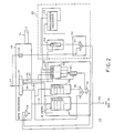
- a data processing system comprising a central processing unit (CPU) 10, a main memory 11, and a buffer memory device 12 to which this invention is applicable and which is intermediate between the central processing unit 10 and the main memory 11.
- the buffer memory device 12 is connected to the central processing unit 10 through a request line 14 and a reply line 15 on one hand and is connected to the main memory 11 through a main memory access line 16 and a block data line 17 on the other hand.
- Each line 14, 15, 16, and 17 is composed of a plurality of electrical conductors, although it is depicted at a single line in Fig. 1.
- the central processing unit 10 supplies either an operand request or an instruction request to the cache memory 12 through the request line 14.
- the operand request is produced either as an operand readout request or as an operand write-in request and is given to the buffer memory device 12 as an operand fetch request.
- the instruction request may be produced either as an instruction readout request or an instruction write-in request is given to the buffer memory device 12 as an instruction fetch request.
- Each of the operand fetch request and the instruction fetch request comprises a request signal representative of whether a request in question is the operand fetch request or the instruction request and a memory address signal specifying a memory address of the main memory 11.
- each request also comprises a flag signal representative of either the readout request or the write-in request.
- the buffer memory device 12 supplies the central processing unit 10 with a reply which includes a reply signal indicative of presence or absence of a data signal required by each fetch request, if the required data signal is memorized in the buffer memory device 12. In this event, the required data signal is sent together with the reply signal through the reply line 15 to the central processing unit 10.
- the main memory 11 is accessed through the buffer memory device 12 and the main memory access line 16. Thereafter, data transfer is carried out from the main memory 11 to the buffer memory device 12 through the block data line 17 to transfer the required data signal through the block data line 17. The required data signal is thus held in the buffer memory device 12 on one hand and is transferred to the central processing unit 10 on the other hand.
- the write-in request be issued as either the operand fetch request or the instruction fetch request through the request line 14 from the central processing unit 10 to the buffer memory device 12.
- the write-in request is specified by the request signal indicative of either the instruction or the operand fetch request, the flag signal representative of the write-in request, and the memory address signal together with a write-in data signal.
- the memory address is indicative of a write-in address. If the write-in data signal can be memorized in the buffer memory device 12, the write-in data signal is memorized in the buffer memory device 12. Otherwise, data transfer is carried out from the main memory 11 to the buffer memory device 12 through the block data line 17 to memorize a data block corresponding to the write-in address signal. In this event, the write-in data signal is also memorized in the main memory 11.
- the request line 14 is used in common to both the operand and the instruction fetch requests, different lines may be individually used for the operand and the instruction fetch requests.
- the readout request be issued from the central processing unit 10 through the request line 14 to the buffer memory device 12.
- the readout request is specified by the request signal, the flag signal representative of the readout request, and the memory address signal representative of a readout memory address.
- the buffer memory device 12 reads a readout data signal out of the readout memory address, if the readout memory address is present in the buffer memory device 12. Otherwise, the readout data signal is read out of the main memory 11 to be sent through the buffer memory device 12 to the central processing unit 10. In this case, a data block which includes the readout data signal is transferred from the main memory 11 to the buffer memory device 12.
- the data transfer is carried out at every one of data blocks between the buffer memory device 12 and the main memory 11.
- the data blocks are individually determined for the operand data signal and the instruction data signal which have different block sizes, respectively.
- the block size for the instruction data signal will be called an instruction block size while the block size for the operand data signal will be called an operand block size.
- the instruction block size is equal to N times the operand block size where N is an integer greater than unity. Specifically, let N be equal to 2 n where n is a natural number. Usually, n may be, for example, two and the instruction block size is therefore equal to four times the operand block size.
- a buffer memory device 12 comprises a data processor 21, a cache memory 22, and a monitoring circuit 23. More particularly, the data processor 21 is connected to the central processing unit 10 through the request line 14 and to the main memory 11 through the main memory address line 16 and the block data line 17. In this connection, the illustrated data processor 21 is supplied with either the operand fetch request or the instruction fetch request from the central processing unit 10 through the request line 14. Each of the operand and the instruction fetch requests includes the request signal, the address signal, and the flag signal, as mentioned before.
- the address signal specifies a required address of the main memory 11.
- the request signal is representative of either the operand fetch request or the instruction fetch request and is held in a first register 26.
- the request signal serves to practically indicate either the operand block size or the instruction block size and may be therefore recognized in the buffer memory device 12 as a block information signal which is indicative of each block size of the operand and the instruction data signals.
- the request signal or block information signal takes a logic "0" level and a logic "1" level in the operand and the instruction fetch requests, respectively.
- the flag signal is not directly concerned with this invention and will not be described any longer.
- either the operand or the instruction data signals is included in the operand or the instruction fetch request when each fetch request is the write-in request, although the following description will mainly be restricted to the readout request.
- the operand and the instruction data signals are delivered from the central processing unit 10 (Fig. 1) to the cache memory 22 through the data processor 21 and a data registration line 31 when the write-in request is given to the data processor 21.
- the address signal is held in a second or address register 27 of the data processor 21 and is divisible into a first significant part of higher significant bits, a second significant part of significant bits lower than those of the first significant part, and a remaining part.
- the illustrated second significant part is subdivided into higher and lower local significant parts.
- the lower local significant part is composed of two bits in the illustrated example.
- the first and the second significant parts are delivered to the cache memory 22 through first and second internal address lines 33 and 34, respectively.
- the higher and the lower local significant parts are sent to the cache memory 22 through third and fourth internal address lines 36 and 37, respectively.
- the higher local significant part may be called an instruction set address for each instruction data block, as will become clear as the description proceeds.
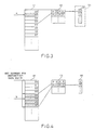
- the cache memory 22 comprises a data buffer 41 having an address space specifiable by the second significant part of the address signal kept in the second register 27.
- the data buffer 41 has a plurality of cache areas the number of which may be determined by a bit number of the second significant part of the address signal, namely, the address space and each of which has a memory capacity M of, for example, 128 bytes.
- the cache areas are consecutively numbered from a zeroth cache area D0 to a last cache area.
- the data buffer 41 is supplied with either the operand or the instruction data signal through the data registration line 31 and is also supplied from the second register 27 with the second significant part through the first internal address line 33. As a result, either the operand data signal or the instruction data signal is memorized in the buffer memory 41 in response to the readout request in a manner to be described later.
- An address buffer 42 is included in the cache memory 22 and is connected to the second register 27 through the first and the second internal address lines 33 and 34.
- the illustrated address buffer 27 has a plurality of address buffer areas which are equal in number to the cache areas and which are accessible by the second significant part of the address signal.
- the address buffer areas are consecutively numbered from a zeroth address buffer area A0 to a last address buffer area in one-to-one correspondence to the cache areas.
- the address buffer areas are loaded with first significant parts in the respective address buffer areas indicated by second significant parts of address signals previously given through the second register 27, in response to previous requests, issued from the central processing unit 10.
- the cache memory 22 further comprises a validity information signal buffer 43 for memorizing a validity information signal V in every one of validity buffer addresses in a manner to be mentioned later.
- the validity information signal buffer 43 is connected to the second register 27 through the third and the fourth internal address lines 36 and 37 to be accessed by the higher and the lower local significant parts of the address signal and to produce four bits of the validity information signals in parallel.
- the four bits of the validity information signals are sent to a selector 44 supplied with the lower local significant part of the address signal from the second register 27.
- the cache memory 22 comprises a comparator 45 connected to the second register 27 through the first internal address line 33 and to the address buffer 42 and an AND gate 46 connected to the comparator 45 and the selector 44.
- the monitoring circuit 23 is operable in cooperation with the data processor 21 to monitor the cache memory 22.
- the illustrated monitoring circuit 23 comprises a block information circuit 51 connected to the data processor 21 through the third internal address line 36 and the data registration line 31, a comparator circuit 52 connected to the block information circuit 51 and the first register 26, and an invalidation processor 53 connected to the data processor 21, the block information circuit 51, and the validity information signal buffer 43. All of the block information circuit 51, the comparator circuit 52, and the invalidation processor 53 will be described more in detail.
- the comparator circuit 52 is connected together with the AND gate 46 to an AND gate circuit 55 included in the data processor 21.
- the instruction block size of the instruction data block is equal to N times, for example, four times the operand block size, as mentioned in conjunction with Fig. 1.
- each of the cache areas of the data buffer 41 can be loaded with a single one of the operand data blocks.
- each of the instruction data blocks is memorized in a plurality of the cache areas of the data buffer 41, for example, four of the cache areas.
- the illustrated buffer memory device 12 selectively carries out an operation in response to the operand fetch request and the instruction fetch request. In this event, it is to be noted that the operand and the instruction fetch requests are dealt with in the buffer memory device 12 in different manners to be presently described.
- a required operand data block is assumed to be transferred from the main memory 11 to the buffer memory device 12 in response to a required one of the operand fetch requests. Such data transfer is carried out as a result of absence of the required operand data block in the cache memory 22.
- the first register 26 is loaded with the block information signal of the logic "0" level representative of the operand fetch request while the second register 27 is loaded with a required operand address which is divisible into the first significant part, the second significant part, and the remaining part, as mentioned above, and in which a required operand data signal is memorized.
- the first and the second significant parts of the required operand address are delivered to the main memory 11 through the main memory access line 16 to read the required operand data block out of the main memory 11.
- the required operand data block which includes the required operand data signal is sent to the data buffer 41 through the block data line 17, the data processor 21, and the data registration line 31.
- the required operand data block is memorized in one of the cache areas that is specified by the second significant part of the required operand address.
- the address buffer 42 is loaded with the first significant part of the required operand address in response to the second significant part thereof.
- a validity information signal is accompanied by the required operand data block and is stored in the validity information signal buffer 43 in accordance with the second significant part of the required operand address while a block information signal of the logic "0" level is also accompanied by the required operand data block and is stored in the block information storage 60 in accordance with the higher local significant part.
- the first register 26 is loaded with the logic "1" level while the second register 27 is loaded with a required instruction address which is also divisible into the first and the second significant parts and the remaining part.
- a required instruction data signal is assumed to be stored in the required instruction address.
- the data processor 21 On transfer of the required instruction data block, the data processor 21 is supplied with the required instruction data block from the main memory 11. To this end, the main memory 11 is accessed to read the required instruction data block out of four main memory areas corresponding to the cache areas. Such a readout operation can be carried out by the use of a known technique. At any rate, the required instruction data block is successively written into four consecutive cache areas in accordance with that second significant part of the required instruction address which indicates a leading one of the cache areas for memorizing the required instruction data block. Concurrently, the address buffer 42 is loaded with the first significant part of the required instruction address in four consecutive address areas which are in one-to-one correspondence to the four consecutive cache areas.
- the validity information signals of the logic "1" levels are accompanied by the required data block and are memorized in four columns of a row of the validity information signal buffer 43 with reference to the higher and the lower significant parts of the required instruction address.
- the block information signal of the logic "1" level is stored in the block information storage 60.
- the first cache area D1 of the data buffer 41 is loaded with one of the operand data blocks as a memorized operand data block of the M bytes, as depicted at a hatched portion in the data buffer 41 of Fig. 3.
- the validity information signal buffer 43 has the validity buffer addresses which are in one-to-one correspondence to the respective cache areas to memorize the validity information signals of single bits.
- four bits of the validity information signals are arranged in each row. Four bits of an uppermost or zeroth one of the rows are made to correspond to the zeroth through the third cache areas D0 to D3, respectively.
- a second column of the zeroth row in the validity buffer addresses of the validity information signal buffer 43 is loaded with the validity information signal of the logic "1" level representative of validity of the one of the operand data blocks memorized in the first cache area D1, as shown by a hatched portion in the validity information signal buffer 43.
- the logic "0" levels are memorized to indicate absence of valid data blocks in the corresponding cache areas.
- Such a validity information signal is sent from the data processor 21 through the data registration line 31 (Fig. 1) to the validity information signal buffer 43 accessed by the higher local significant part through the third internal address line 36.
- a single row of the validity information signal buffer 43 is simultaneously accessed by the higher local significant part. This shows that a single one of the validity buffer addresses in each row is not specified by the higher local significant part of the address signal.
- an enable signal (not shown) is also given from the data processor 21 or the lower significant part may be given to the validity information signal buffer 43.
- the block information circuit 51 is specified by a block information storage 60 having a plurality of storage addresses which may be equal in number to the rows of the validity information signal buffer 43.
- a block information signal is stored so as to specify whether each row of the validity information signal buffer 43 is loaded with the operand data block or the instruction data block.
- the logic "0" level is stored in an uppermost or zeroth one of the storage addresses when at least one of the operand data blocks is memorized in the row of the validity information signal buffer 43.
- the logic "1" level is stored in each storage address when the instruction data block is memorized in each row of the validity information signal buffer 43.
- the logic "0" level is stored in each storage address of the block information storage 60 even when one of the operand data blocks is memorized in the row. This means that the logic "0" level of each storage address is kept unchanged when four operand data blocks are memorized in the cache areas corresponding to each row of the validity information signal buffer 43.
- Such a block information signal can be stored in each storage address of the block information storage 60 by supplying the block information storage 60 with the higher local significant part and the block information signal which is included in each of the operand and the instruction fetch requests and which is sent from the data processor 21 through the data registration line 31.
- the block information signal may be delivered from the first register 26 to the block information storage 60.
- an uppermost or zeroth one of the storage addresses in the block information storage 60 is loaded with the logic "0" level to indicate storage of the operand data block, as illustrated in Fig. 3.
- the data buffer 41, the validity information signal buffer 43, and the block information storage 60 are put into the illustrated states.
- the operand fetch request is assumed to be the readout request and to be issued as a required operand request from the central processing unit 10 (Fig. 1) to the data processor 21 (Fig. 2).
- the first significant part of a required address signal is sent as an operand access signal (depicted at a in Fig. 3) from the second register 27 to the data buffer 41 to access the first cache area D1 of the data buffer 41.
- the higher local significant part of the address signal is delivered from the second register 27 to the validity information signal buffer 43 through the third internal address line 36 to specify the uppermost or zeroth row of the validity information signal buffer 43.
- the validity information signals are concurrently read out of the zeroth row of the validity information signal buffer 43 to be sent to the selector 44 which is supplied with the lower local significant part of two bits.
- the selector 44 (Fig. 1) selects the validity information signal of the logic "1" level as a selected validity information signal in response to the lower local significant part in the example being illustrated.
- the selected validity information signal of the logic "1" level is sent to the AND gate 46.
- the address buffer areas of the address buffer 42 are loaded with those first significant parts of the address signals which correspond to the operand and the instruction data blocks memorized in the data buffer 41 and which may be referred to as first memorized parts. Responsive to the second significant part which specifies the first address buffer area and which is sent from the second register 27, the address buffer 42 produces the first memorized part memorized in the first address buffer area. The first memorized part is delivered from the address buffer 42 to the comparator 45 supplied with the first significant part sent from the second register 27. The comparator 45 compares the first memorized part with the first significant part held in the second register 27 to produce an address coincidence signal of the logic "1" level when the first memorized part is coincident with the first significant part.
- the AND gate 46 delivers a gate output signal of the logic "1" level to the AND gate circuit 55 of the data processor 21 (Fig. 1).
- the gate output signal of the logic "1" level is indicative of presence of a requested data block in the cache memory 22 and may be called a bit signal.
- the gate output signal of the logic "0" level is indicative of absence of a requested data block and may be called a mishit signal.
- the block information storage 60 is accessed by the higher local significant part of the address signal held in the second register 27.
- the block information signal of the logic "0" level is read out of the zeroth one of the storage areas of the block information storage 60 as a specific block information signal to indicate storage of the operand data block, as shown in Fig. 3.
- the specific block information signal is delivered from the block information storage 60 to the invalidation processor 53 on one hand and to the comparator circuit 52 on the other hand.
- the comparator circuit 52 comprises a comparator unit 63 connected to the block information storage 60 and the first register 26 of the data processor 21, as shown in Fig. 1.
- the comparator unit 63 is therefore supplied with the block information signal and the specific block information signal from the first register 26 and the block information storage 60, respectively.
- the comparator unit 63 supplies the AND gate circuit 55 with a block coincident signal of the logic "1" level indicative of coincidence between the requested block information signal and the specific block information signal. Otherwise, an incoincident signal of the logic "0" level is sent from the comparator unit 63 to the AND gate circuit 55.
- the AND gate circuit 55 supplies the central processing unit 10 (Fig. 1) as the reply signal with a logic "1" level signal indicative of presence of a required operand data block in the cache memory 22.
- the required operand data block is read out of the first cache address of the data buffer 41 and is transferred through the reply line 15 to the central processing unit 10.
- Fig. 4 together with Fig. 1, it is assumed that the fourth through seventh cache areas D4 to D7 of the data buffer 41 are loaded with an instruction data block, as indicated by a hatched portion, and that four columns of the first row in the validity information buffer 43 are loaded with the validity information signals of the logic "1" levels, respectively.
- the instruction block size occupies four cache areas of the data buffer 41, as mentioned before.
- the first one of the storage addresses in the block information storage 60 is loaded as the block information signal with the logic "1" level so as to specify storage of the instruction data block in the fourth through the seventh cache areas of the data buffer 41.
- the instruction fetch request be the readout request and issued as a required instruction request from the central processing unit 10 to the buffer memory device 12 (Fig. 2).
- the second significant part of a required address signal included in the required instruction request is sent from the second register 27 to the data buffer 41 and the address buffer 42.
- the first significant part is delivered from the address register 27 to the comparator circuit 45.
- the higher and the lower local significant parts of the required address signal are sent from the address register 27 to the validity information signal buffer 43 and the selector 44, as mentioned in conjunction with Fig. 3.
- a first significant part is read as a first memorized part out of the first address area A1 of the address buffer 42 to be sent to the comparator circuit 45 and is compared with the first significant part of the required address signal.
- the validity information signals of the logic "1" levels are read out of the first row of the validity information signal buffer 43 to be sent to the selector 44.
- the selector 44 selects one of the validity information signals that is delivered to the AND gate 46.
- the first one of the storage addresses in the block information storage 60 is loaded with the block information signal of the logic "1" level to specify storage of the instruction data block, as shown in Fig. 4.
- the comparator circuit 63 supplies the AND gate circuit 55 with the logic "1" level. Therefore, the data processor 21 gives the central processing unit 10 the reply signal of the logic "1" level representative of presence of the instruction data block in question.
- the data buffer 41 is given the second significant part of the address signal as an instruction access signal (depicted at b in Fig. 4). Accordingly, the instruction data signal in question is read out of the first cache area A1 of the data buffer 41 to be sent to the central processing unit 10. Alternatively, the instruction data block may be transferred from the data buffer 41 to the central processing unit 10.
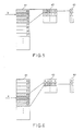
- an operand data block be previously memorized in the first cache area of the data buffer 41, like in Fig. 3.
- a required instruction fetch request is issued from the central processing unit 10 (Fig. 10) in the form of an instruction access signal (depicted at b like in Fig. 4) which indicates the first cache area of the data buffer 41.
- the comparator unit 63 detects incoincidence between the block information signals sent from the first register 26 and the block information storage 60 to supply the AND gate circuit 55 with the incoincidence signal of the logic "0" level. This shows that a required instruction data block is not present in the data buffer 41. Therefore, the required instruction data block should be read out of the main memory 11 (Fig. 1).
- block data transfer of the instruction data block in question is carried out between the main memory 11 and the buffer memory device 12 through the block data line 17 (Figs. 1 and 2) in the manner mentioned before.
- a leading one of the cache areas for the required instruction data block is kept in the second register 27 of the data processor 21 (Fig. 2).
- the required instruction data block is written into the leading cache area and is thereafter continuously written into three consecutive cache areas following the leading cache area.
- two least significant bits of the address signal kept in the second register 27 may be neglected during such a write-in operation.
- the zeroth cache area is indicated as the leading cache area.
- the required instruction data block is loaded with the zeroth through third cache areas D1 to D3, as shown in Fig. 5.
- the four columns of the zeroth row in the validity information signal buffer 43 are concurrently loaded with the validity information signals of the logic "1" levels, as illustrated in Fig. 5, while the zeroth storage address of the block information storage 60 is loaded with the block information signal of the logic "1" level to indicate storage of the instruction data block.
- the first significant part kept in the address register 27 is simultaneously written into the zeroth through third address buffer areas A0 to A3 through the first internal address line 33.
- Such a simultaneous write-in operation can be carried out in a known manner and will not be described any longer.
- Fig. 6 in addition to Fig. 2, it is assumed that the fourth through seventh cache areas of the data buffer 41 are loaded with a previous instruction data block and that the four columns of the first row of the validity information signal buffer 43 are loaded with the validity information signals of the logic "1" levels, respectively.
- the first storage address of the block information storage 60 is previously loaded with the logic "1" level so as to indicate storage of the previous instruction data block in the fourth through seventh cache areas D4 to D7 of the data buffer 41.
- an operand fetch request be issued from the central processing unit 10 to the buffer memory device 12 to access the fifth cache area D5 in the form of an operand access signal (depicted at a in Fig. 6) by indicating an operand data block which may be called a required operand data block.
- an incoincidence signal is sent from the comparator unit 63 to the AND gate circuit 55 to indicate absence of the required operand data block.
- the required operand data block is transferred from the main memory 11 to the fifth cache area D5 of the data buffer 41, as shown by a cross-hatched portion in Fig. 6.
- the validity information signals of the logic "1" levels in the first row of the validity information signal buffer 43 should be rewritten, as illustrated in a cross-hatched portion of the validity information signal buffer 43, together with the first storage address of the block information storage 60.
- the invalidation processor 53 is used to rewrite validity information signals memorized in the validity information signal buffer 43. More specifically, the invalidation processor 53 is supplied with the block information signal and the first significant part of the operand fetch request from the block information storage 60 and the data processor 21, respectively. The invalidation processor 53 delivers an invalidation signal to the validity information signal buffer 43. The invalidation signal is stored in three columns of the first row in the validity information signal buffer 43 under control of the data processor, as shown in Fig. 6. Thus, the validity information signals of the first row are rewritten into (0100). The first storage address of the block information storage is loaded with the logic "0" level to indicate storage of an operand data block in response to the operand fetch request.
- the data buffer 41 can be loaded with both the operand and the instruction data blocks having different data block sizes in common.
- both the operand and the instruction data blocks can be independently processed in such a common data buffer 41.
- a plurality of cache memories similar in structure and operation to that illustrated in Fig. 2 may be arranged in different levels.
- the instruction data block size may not always be equal to 2 n times the operand data block size.
Landscapes
- Engineering & Computer Science (AREA)
- Theoretical Computer Science (AREA)
- Software Systems (AREA)
- Physics & Mathematics (AREA)
- General Engineering & Computer Science (AREA)
- General Physics & Mathematics (AREA)
- Memory System Of A Hierarchy Structure (AREA)
- Advance Control (AREA)
Applications Claiming Priority (2)
| Application Number | Priority Date | Filing Date | Title |
|---|---|---|---|
| JP63119352A JP2818415B2 (ja) | 1988-05-18 | 1988-05-18 | バッファ記憶装置 |
| JP119352/88 | 1988-05-18 |
Publications (3)
| Publication Number | Publication Date |
|---|---|
| EP0342631A2 true EP0342631A2 (de) | 1989-11-23 |
| EP0342631A3 EP0342631A3 (de) | 1991-09-18 |
| EP0342631B1 EP0342631B1 (de) | 1997-09-24 |
Family
ID=14759366
Family Applications (1)
| Application Number | Title | Priority Date | Filing Date |
|---|---|---|---|
| EP89108845A Expired - Lifetime EP0342631B1 (de) | 1988-05-18 | 1989-05-17 | Pufferspeicher, der zur Speicherung von Befehls- und Datenblöcken auf verschiedene Blockgrössen geeignet ist |
Country Status (5)
| Country | Link |
|---|---|
| US (1) | US5109498A (de) |
| EP (1) | EP0342631B1 (de) |
| JP (1) | JP2818415B2 (de) |
| AU (1) | AU617474B2 (de) |
| DE (1) | DE68928333T2 (de) |
Cited By (1)
| Publication number | Priority date | Publication date | Assignee | Title |
|---|---|---|---|---|
| EP0838752A3 (de) * | 1996-09-26 | 1999-05-26 | Nokia Mobile Phones Ltd. | Kommunikationsgerät |
Families Citing this family (17)
| Publication number | Priority date | Publication date | Assignee | Title |
|---|---|---|---|---|
| US6112287A (en) * | 1993-03-01 | 2000-08-29 | Busless Computers Sarl | Shared memory multiprocessor system using a set of serial links as processors-memory switch |
| JPH0740247B2 (ja) * | 1989-06-20 | 1995-05-01 | 松下電器産業株式会社 | キャッシュメモリ装置 |
| US5442769A (en) * | 1990-03-13 | 1995-08-15 | At&T Corp. | Processor having general registers with subdivisions addressable in instructions by register number and subdivision type |
| US6324120B2 (en) | 1990-04-18 | 2001-11-27 | Rambus Inc. | Memory device having a variable data output length |
| US6751696B2 (en) * | 1990-04-18 | 2004-06-15 | Rambus Inc. | Memory device having a programmable register |
| IL96808A (en) | 1990-04-18 | 1996-03-31 | Rambus Inc | Introductory / Origin Circuit Agreed Using High-Performance Brokerage |
| US5390304A (en) * | 1990-09-28 | 1995-02-14 | Texas Instruments, Incorporated | Method and apparatus for processing block instructions in a data processor |
| US5822781A (en) * | 1992-10-30 | 1998-10-13 | Intel Corporation | Sector-based storage device emulator having variable-sized sector |
| FR2732134B1 (fr) * | 1995-03-23 | 1997-06-06 | Suisse Electronique Microtech | Systeme informatique avec memoires hierarchisees |
| US5737550A (en) * | 1995-03-28 | 1998-04-07 | Advanced Micro Devices, Inc. | Cache memory to processor bus interface and method thereof |
| US6782469B1 (en) | 2000-09-29 | 2004-08-24 | Intel Corporation | Runtime critical load/data ordering |
| US6760816B1 (en) * | 2000-09-29 | 2004-07-06 | Intel Corporation | Critical loads guided data prefetching |
| US6662273B1 (en) | 2000-09-29 | 2003-12-09 | Intel Corporation | Least critical used replacement with critical cache |
| AU2002360640A1 (en) * | 2002-12-17 | 2004-07-29 | International Business Machines Corporation | Selectively changeable line width memory |
| JP2005166155A (ja) * | 2003-12-02 | 2005-06-23 | Hitachi-Lg Data Storage Inc | 光ディスクドライブ装置 |
| US7958436B2 (en) | 2005-12-23 | 2011-06-07 | Intel Corporation | Performing a cyclic redundancy checksum operation responsive to a user-level instruction |
| US7925957B2 (en) | 2006-03-20 | 2011-04-12 | Intel Corporation | Validating data using processor instructions |
Family Cites Families (7)
| Publication number | Priority date | Publication date | Assignee | Title |
|---|---|---|---|---|
| US4312036A (en) * | 1978-12-11 | 1982-01-19 | Honeywell Information Systems Inc. | Instruction buffer apparatus of a cache unit |
| US4315312A (en) * | 1979-12-19 | 1982-02-09 | Ncr Corporation | Cache memory having a variable data block size |
| US4575814A (en) * | 1982-05-26 | 1986-03-11 | Westinghouse Electric Corp. | Programmable interface memory |
| JPH0673114B2 (ja) * | 1987-03-31 | 1994-09-14 | 日本電気株式会社 | キヤツシユ制御装置 |
| US4908748A (en) * | 1987-07-28 | 1990-03-13 | Texas Instruments Incorporated | Data processing device with parallel circular addressing hardware |
| JPH01173241A (ja) * | 1987-12-28 | 1989-07-07 | Toshiba Corp | キャッシュメモリ装置 |
| US5025366A (en) * | 1988-01-20 | 1991-06-18 | Advanced Micro Devices, Inc. | Organization of an integrated cache unit for flexible usage in cache system design |
-
1988
- 1988-05-18 JP JP63119352A patent/JP2818415B2/ja not_active Expired - Lifetime
-
1989
- 1989-05-17 EP EP89108845A patent/EP0342631B1/de not_active Expired - Lifetime
- 1989-05-17 DE DE68928333T patent/DE68928333T2/de not_active Expired - Fee Related
- 1989-05-17 US US07/353,361 patent/US5109498A/en not_active Expired - Fee Related
- 1989-05-18 AU AU34912/89A patent/AU617474B2/en not_active Ceased
Cited By (2)
| Publication number | Priority date | Publication date | Assignee | Title |
|---|---|---|---|---|
| EP0838752A3 (de) * | 1996-09-26 | 1999-05-26 | Nokia Mobile Phones Ltd. | Kommunikationsgerät |
| US6285888B1 (en) | 1996-09-26 | 2001-09-04 | Nokia Mobile Phones, Ltd. | Mobile telephone arranged to receive and transmit digital data samples of encoded speech |
Also Published As
| Publication number | Publication date |
|---|---|
| US5109498A (en) | 1992-04-28 |
| DE68928333T2 (de) | 1998-01-29 |
| JP2818415B2 (ja) | 1998-10-30 |
| JPH01290050A (ja) | 1989-11-21 |
| AU3491289A (en) | 1989-11-23 |
| DE68928333D1 (de) | 1997-10-30 |
| EP0342631B1 (de) | 1997-09-24 |
| AU617474B2 (en) | 1991-11-28 |
| EP0342631A3 (de) | 1991-09-18 |
Similar Documents
| Publication | Publication Date | Title |
|---|---|---|
| US5109498A (en) | Buffer memory device capable of memorizing operand and instruction data blocks at different block sizes | |
| US4991081A (en) | Cache memory addressable by both physical and virtual addresses | |
| US4471429A (en) | Apparatus for cache clearing | |
| US5091851A (en) | Fast multiple-word accesses from a multi-way set-associative cache memory | |
| US5450564A (en) | Method and apparatus for cache memory access with separate fetch and store queues | |
| US6295580B1 (en) | Cache system for concurrent processes | |
| US4916604A (en) | Cache storage apparatus | |
| US5740400A (en) | Reducing cache snooping overhead in a multilevel cache system with multiple bus masters and a shared level two cache by using an inclusion field | |
| US6098150A (en) | Method and apparatus for fetching information from a cache memory | |
| EP0347040A1 (de) | Datenspeicheranordnung | |
| EP0167089B1 (de) | Speicherzugriffs-Steuerungssystem und -Verfahren für ein Informationsverarbeitungsgerät | |
| CA1159153A (en) | Apparatus for cache clearing | |
| US4949244A (en) | Storage system | |
| EP0180369B1 (de) | Durch beide, physikalische und virtuelle Addressen, addressierbarer Cache-Speicher | |
| CA1202426A (en) | Buffer storage including a swapping circuit | |
| EP0173909A2 (de) | LRU-Markiersteuerungsschaltung für look-aside Puffer | |
| US6901450B1 (en) | Multiprocessor machine and cache control method for providing higher priority to shared cache that is accessed by multiprocessors | |
| US4644539A (en) | Circuit arrangement capable of prohibiting an access to a part of a control memory on occurrence of an error in the part | |
| EP0055579B1 (de) | Cache-Speicher mit Doppelwort-Zugriff | |
| US5544293A (en) | Buffer storage system and method using page designating address and intra-page address and detecting valid data | |
| US5535358A (en) | Cache memory control circuit and method for controlling reading and writing requests | |
| US4602329A (en) | Data processing system having an address translation unit shared by a CPU and a channel unit | |
| EP0173556A2 (de) | Hierarchische Architektur zur Bestimmung von dem am wenigsten kürzlich benutzten Cachespeicher | |
| EP0335113A2 (de) | Einchip-Cache-Speicher und Cache-Speichervorrichtung mit mehreren parallel geschalteten Einchip-Cache-Speichern | |
| EP0287844A2 (de) | Cache-Speicherschaltung mit Speichern mit Doppelzugriffseinrichtung |
Legal Events
| Date | Code | Title | Description |
|---|---|---|---|
| PUAI | Public reference made under article 153(3) epc to a published international application that has entered the european phase |
Free format text: ORIGINAL CODE: 0009012 |
|
| 17P | Request for examination filed |
Effective date: 19890614 |
|
| AK | Designated contracting states |
Kind code of ref document: A2 Designated state(s): DE FR GB IT NL SE |
|
| PUAL | Search report despatched |
Free format text: ORIGINAL CODE: 0009013 |
|
| AK | Designated contracting states |
Kind code of ref document: A3 Designated state(s): DE FR GB IT NL SE |
|
| 17Q | First examination report despatched |
Effective date: 19941122 |
|
| GRAG | Despatch of communication of intention to grant |
Free format text: ORIGINAL CODE: EPIDOS AGRA |
|
| GRAH | Despatch of communication of intention to grant a patent |
Free format text: ORIGINAL CODE: EPIDOS IGRA |
|
| GRAH | Despatch of communication of intention to grant a patent |
Free format text: ORIGINAL CODE: EPIDOS IGRA |
|
| GRAA | (expected) grant |
Free format text: ORIGINAL CODE: 0009210 |
|
| AK | Designated contracting states |
Kind code of ref document: B1 Designated state(s): DE FR GB IT NL SE |
|
| REF | Corresponds to: |
Ref document number: 68928333 Country of ref document: DE Date of ref document: 19971030 |
|
| ITF | It: translation for a ep patent filed | ||
| ET | Fr: translation filed | ||
| PLBE | No opposition filed within time limit |
Free format text: ORIGINAL CODE: 0009261 |
|
| STAA | Information on the status of an ep patent application or granted ep patent |
Free format text: STATUS: NO OPPOSITION FILED WITHIN TIME LIMIT |
|
| 26N | No opposition filed | ||
| PGFP | Annual fee paid to national office [announced via postgrant information from national office to epo] |
Ref country code: SE Payment date: 19990510 Year of fee payment: 11 |
|
| PGFP | Annual fee paid to national office [announced via postgrant information from national office to epo] |
Ref country code: FR Payment date: 19990511 Year of fee payment: 11 |
|
| PGFP | Annual fee paid to national office [announced via postgrant information from national office to epo] |
Ref country code: GB Payment date: 19990512 Year of fee payment: 11 |
|
| PGFP | Annual fee paid to national office [announced via postgrant information from national office to epo] |
Ref country code: DE Payment date: 19990514 Year of fee payment: 11 |
|
| PGFP | Annual fee paid to national office [announced via postgrant information from national office to epo] |
Ref country code: NL Payment date: 19990531 Year of fee payment: 11 |
|
| PG25 | Lapsed in a contracting state [announced via postgrant information from national office to epo] |
Ref country code: GB Free format text: LAPSE BECAUSE OF NON-PAYMENT OF DUE FEES Effective date: 20000517 |
|
| PG25 | Lapsed in a contracting state [announced via postgrant information from national office to epo] |
Ref country code: SE Free format text: LAPSE BECAUSE OF NON-PAYMENT OF DUE FEES Effective date: 20000518 |
|
| PG25 | Lapsed in a contracting state [announced via postgrant information from national office to epo] |
Ref country code: NL Free format text: LAPSE BECAUSE OF NON-PAYMENT OF DUE FEES Effective date: 20001201 |
|
| GBPC | Gb: european patent ceased through non-payment of renewal fee |
Effective date: 20000517 |
|
| EUG | Se: european patent has lapsed |
Ref document number: 89108845.2 |
|
| PG25 | Lapsed in a contracting state [announced via postgrant information from national office to epo] |
Ref country code: FR Free format text: LAPSE BECAUSE OF NON-PAYMENT OF DUE FEES Effective date: 20010131 |
|
| NLV4 | Nl: lapsed or anulled due to non-payment of the annual fee |
Effective date: 20001201 |
|
| PG25 | Lapsed in a contracting state [announced via postgrant information from national office to epo] |
Ref country code: DE Free format text: LAPSE BECAUSE OF NON-PAYMENT OF DUE FEES Effective date: 20010301 |
|
| REG | Reference to a national code |
Ref country code: FR Ref legal event code: ST |
|
| PG25 | Lapsed in a contracting state [announced via postgrant information from national office to epo] |
Ref country code: IT Free format text: LAPSE BECAUSE OF NON-PAYMENT OF DUE FEES;WARNING: LAPSES OF ITALIAN PATENTS WITH EFFECTIVE DATE BEFORE 2007 MAY HAVE OCCURRED AT ANY TIME BEFORE 2007. THE CORRECT EFFECTIVE DATE MAY BE DIFFERENT FROM THE ONE RECORDED. Effective date: 20050517 |