EP0342107A2 - Flagge für einen FIFO - Google Patents
Flagge für einen FIFO Download PDFInfo
- Publication number
- EP0342107A2 EP0342107A2 EP89401270A EP89401270A EP0342107A2 EP 0342107 A2 EP0342107 A2 EP 0342107A2 EP 89401270 A EP89401270 A EP 89401270A EP 89401270 A EP89401270 A EP 89401270A EP 0342107 A2 EP0342107 A2 EP 0342107A2
- Authority
- EP
- European Patent Office
- Prior art keywords
- signal
- write
- logic state
- read
- response
- Prior art date
- Legal status (The legal status is an assumption and is not a legal conclusion. Google has not performed a legal analysis and makes no representation as to the accuracy of the status listed.)
- Granted
Links
- 230000004044 response Effects 0.000 claims abstract description 26
- 230000007704 transition Effects 0.000 claims abstract description 16
- 230000008859 change Effects 0.000 claims description 8
- 230000002401 inhibitory effect Effects 0.000 claims description 5
- 238000000926 separation method Methods 0.000 abstract description 2
- 230000001934 delay Effects 0.000 abstract 1
- 230000000630 rising effect Effects 0.000 description 33
- 238000010586 diagram Methods 0.000 description 16
- 230000015654 memory Effects 0.000 description 13
- 230000006870 function Effects 0.000 description 12
- 230000003111 delayed effect Effects 0.000 description 3
- 230000004075 alteration Effects 0.000 description 1
- 230000000903 blocking effect Effects 0.000 description 1
- 125000004122 cyclic group Chemical group 0.000 description 1
- 238000006467 substitution reaction Methods 0.000 description 1
- 230000001360 synchronised effect Effects 0.000 description 1
- 230000001960 triggered effect Effects 0.000 description 1
Images


Classifications
-
- G—PHYSICS
- G06—COMPUTING; CALCULATING OR COUNTING
- G06F—ELECTRIC DIGITAL DATA PROCESSING
- G06F5/00—Methods or arrangements for data conversion without changing the order or content of the data handled
- G06F5/06—Methods or arrangements for data conversion without changing the order or content of the data handled for changing the speed of data flow, i.e. speed regularising or timing, e.g. delay lines, FIFO buffers; over- or underrun control therefor
- G06F5/10—Methods or arrangements for data conversion without changing the order or content of the data handled for changing the speed of data flow, i.e. speed regularising or timing, e.g. delay lines, FIFO buffers; over- or underrun control therefor having a sequence of storage locations each being individually accessible for both enqueue and dequeue operations, e.g. using random access memory
- G06F5/12—Means for monitoring the fill level; Means for resolving contention, i.e. conflicts between simultaneous enqueue and dequeue operations
-
- G—PHYSICS
- G11—INFORMATION STORAGE
- G11C—STATIC STORES
- G11C15/00—Digital stores in which information comprising one or more characteristic parts is written into the store and in which information is read-out by searching for one or more of these characteristic parts, i.e. associative or content-addressed stores
-
- G—PHYSICS
- G06—COMPUTING; CALCULATING OR COUNTING
- G06F—ELECTRIC DIGITAL DATA PROCESSING
- G06F2205/00—Indexing scheme relating to group G06F5/00; Methods or arrangements for data conversion without changing the order or content of the data handled
- G06F2205/12—Indexing scheme relating to groups G06F5/12 - G06F5/14
- G06F2205/126—Monitoring of intermediate fill level, i.e. with additional means for monitoring the fill level, e.g. half full flag, almost empty flag
Definitions
- the present invention pertains in general to FIFOs and, more particularly, to the operation of the flags to determine the amount of information stored in the FIFO.
- FIFOs First In First Out Memories
- FIFOs provide an important data buffer function for reading and writing operations between two discrete machines of widely differing operating frequency. FIFOs allow asynchronous operation between the two machines, wherein data can be simultaneously written to the FIFO and read therefrom.
- the heart of the FIFO is a dual-port memory that enables the Read and Write operations to be independent of each other, this allowing truly asynchronous operation of the input and the output.
- the dual-port memory portion of the FIFO can be realized with a dual-port RAM cell that has a plurality of addressable locations.
- the Read and Write pointers are provided for generating the addresses of the addressable locations for the Read and Write operations, respectively.
- the Read and Write pointers are incremented for a Read and Write operation, respectively, instead of actually moving the data through a series of shift registers.
- the status flags are utilized on the Read side to indicate to the user that the FIFO is empty. In this manner, the user would not attempt to read a FIFO that is empty and, in fact, circuitry is provided to inhibit incrementing of the Read pointer to overtake the Write pointer address. In a similar manner, a full flag is provided to indicate to the user that the memory is full, such that the user will not attempt to write data to the memory or increment the pointer past the Read pointer.
- the full and empty status flags are conventional flags that are provided in FIFOs.
- An additional flag that has been provided for FIFOs in the past is a half-full flag that indicates to the Write side of the FIFO that the FIFO is half-full and to the Read side of the FIFO that the FIFO is half-empty.
- this type of flag has some synchronization problems associated therewith, especially when utilized with asynchronous operation. For example, when data is being written into the memory at a location that will set the half-full flag to the half-full position, it is important to insure that a simultaneous Read operation does not result in a flag error wherein the flag is in the wrong state. Typically, a FIFO having 2048 registers would have the half-full flag set when data is written into the 1025th location. However, if a simultaneous Read operation occurs, the half flag can be inadvertently manufactured in the reset portion or in the Write operation that the flag can be return to the reset position.
- the present invention disclosed and claimed herein comprises an almost full flag for a FIFO.
- a Read pointer is provided for determining the location in the FIFO for reading information therefrom and a Write pointer is provided for determining the location in the FIFO for writing information thereto.
- the Read pointer is incremented for each Read operation and the Write pointer is incremented for each Write operation with the Write pointer having a higher value than the Read pointer.
- Counter circuitry is provided for determining the proximity of the Read pointer to the Write pointer. When the Read and Write pointer are separated by a predetermined distance that is less than full and greater than empty, a compare signal is generated at a first logic state. If the compare signal is not generated, the output of the counter circuitry is at a second logic state.
- the counter circuitry has a predetermined settling time after changing states from the first logic state to the second logic state or from the second logic state to the first logic state.
- Blanking circuitry is provided for inhibiting generation of the reset signal until a predetermined duration of time after generation of the external Read signal.
- the external Read signal causes the compare signal to change from the second logic state to the first logic state.
- the counter circuitry has a predetermined settling time.
- the compare signal is latched onto one input of an AND circuit for a predetermined duration of time after receipt of the external Write signal.
- the other input of the AND gate is connected to a pulse having a width equal to the predetermined duration of time such that a set signal is generated only during that predetermined duration of time and is isolated from any change in the output of the counter circuit. Additionally, the reset operation is blanked during the predetermined duration of time.
- the FIFO has a dual-port memory array 10 which has a data input port connected to a bus 12 and a data output port connected to a bus 14.
- the bus 12 is output from an input buffer 16 which is connected to input data D0 ⁇ -D8 on an input bus 18, and the bus 14 is input to an output buffer 20 which provides output data Q0 ⁇ -Q8 on an output bus 22.
- the dual-port memory 10 is an array of addressable memory locations operable to be written to from the bus 12 and read out to the bus 14.
- any type of FIFO memory block such as registers, etc., can be utilized in association with the present invention.
- the memory array 10 has Write address input connected to a Write address pointer 24 through a bus 26.
- the Read address input is connected to the output of the Read address pointer 28 through a bus 30.
- the address pointers 24 and 28 are cyclical counters which are incremented by various control signals.
- the Write address pointer 24 is controlled by a Write control circuit 32 that is connected to a Write input signal and the Read address pointer 28 is controlled by a Read control circuit 34 that receives the Read input signal.
- the next sequential address can be written to for each new data word input to the array 10 and the Read pointer 28 can be incremented to read out data stored at the next sequential address.
- the output of the Write control circuit 32 is input to the input buffer 16, and also to a flag logic circuit 36, which also receives on the input thereof the output of the Read control circuit 34.
- the Read control circuit 34 is also input to the output buffer 20.
- the flag logic circuit 36 is operable to determine the proximity of the Write address pointer 24 and the Read address pointer 28 by internally counting each Write and Read operation and comparing the count values.
- a full flag is output on a line 38 when the Read pointer 28 and Write pointer 24 are at a maximum distance apart and an empty flag is output on a line 40 when the Read pointer 28 and the Write pointer 24 are equal.
- An almost full/almost empty flag is output on a line 42 to indicate a proximity in between empty and full.
- this proximity is half-full.
- This flag is referred to as the half flag.
- the half flag is therefore set when one register more than fifty percent of the addressable locations in the array 10 is written to, which flag indicates to the Write side that the array 10 is half-full. It should be understood that the half flag can be set and reset at any proximity of the two pointers such as, for example, four bytes from empty or eight bytes from full.
- FIG. 2 there is illustrated a schematic block diagram of the flag logic circuit 36 and the portion thereof for generating the half flag on line 42.
- the generation of the full and empty flags on lines 38 and 40 is conventional and will not be described herein in detail.
- the output of the Write control circuit 32 is input to a counter 44 and the output of the Read control 34 is input to a counter 46.
- Counter 44 and counter 46 are cyclical counters which are continually incremented.
- the output of counters 44 and 46 are input to a compare circuit 48.
- the compare circuit 48 generates a match on an output line 50 whenever the counters are separated by a value of 1024. This represents a half-full status wherein the array 10 in the preferred embodiment has a maximum register value of 2048.
- This match signal is input to an almost full flag logic block 52, the output of which provides the half flag on line 42.
- the flag logic circuit 52 also receives the output of the Write control circuit 32 and the output of Read control circuit 34, and is generally operable to set the flag when it is determined that the count value has gone from 1024 to 1025 and to reset the flag when it is determined that the count value is at 1024.
- the flag logic circuit 52 prevents errors from occurring in the status of the half flag when the Read and Write operations occur proximate to the transition between the values 1024 and 1025 and even when the transitions are simultaneous, such that an error in the half flag cannot occur.
- the circuit generally operates by generating a narrow pulse off the trailing edge of the Read signal and a narrow pulse off the trailing edge of the Write signal.
- FIG. 3 there is illustrated a logic diagram of a cyclic eleven-bit counter which makes up each of counters 44 and 46, both counters being identical.
- Each of the eleven bits is comprised of a D-type flip flop 54 with each of the flip flops 54 having the Q-output thereof providing one of the output bits BO0 ⁇ -BO10 ⁇ .
- a second counter (not shown) would provide the values AO0 ⁇ /-AO10 ⁇ , this counter being identical to the counter illustrated in Figure 3.
- the counter is clocked by a clock signal on line 56 and a set input is connected to a reset signal INITB on line 58.
- the counters are initially set to a predetermined value and then the counter clock incremented to the values BO0 ⁇ -BO10 ⁇ .
- the flip flop 54 associated with the bit BO0 ⁇ has the data input thereof connected to V DD through an invertor 60.
- the data input for the flip flop 54 associated with the BO1 bit has the input thereof connected to the output of a NAND gate 62, one input of which is connected to the BO0 ⁇ bit and the other input of which is connected to V DD .
- the data input for the BO2 flip flop 54 is connected to the output of a three-input NAND gate 64, one input of which is connected to the BO1 bit, one input of which is connected to the BO0 ⁇ bit and one input of which is connected to the V DD .
- the BO3 flip flop 54 has the data input thereof connected to the output of a four-input NAND gate 66, one input of which is connected to the BO2 bit, one input of which is connected to the BO1 bit, one input of which is connected to the BO0 ⁇ bit and one input of which is connected to V DD .
- the data input to the BO4 flip flop 54 is connected through an invertor 68 to the output of a NOR gate 70.
- NOR gate 70 has one input thereof connected to the output of a three-input NAND gate 72 and the other input thereof connected to the output of a two-input NAND gate 74.
- NAND gate 72 has one input thereof connected to the BO3 bit, one input thereof connected to the BO2 bit and one input thereof connected to the BO1 bit.
- NAND gate 74 has one input thereof connected to the BO0 ⁇ bit and one input thereof connected to V DD .
- the BO5 flip flop 54 has the data input thereof connected to the output of a NAND gate 76, one input of which is connected to the BO4 bit and one input of which is connected to the output of NOR gate 70.
- the BO6 flip flop 54 has the data input thereof connected to the output of a three-input NAND gate 78, one input of which is connected to the BO5 bit, one input of which is connected to the BO4 bit and one input of which is connected to the output of NOR gate 70.
- the BO7 flip flop 54 has the data input thereof connected to a four-input NAND gate 80, one input of which is connected to the BO6 bit, one input of which is connected to the BO5 bit, one input of which is connected to the BO4 input and one input of which is connected to the output of NOR gate 70.
- the data input to the BO8 flip flop 54 is connected through an invertor 82 to the output of a NOR gate 84.
- NOR gate 84 has one input thereof connected to the output of a three-input NAND gate 86 and one input thereof connected to the output of two-input NAND gate 88.
- NAND gate 86 has one input thereof connected to the BO7 bit, one input thereof connected to the BO6 bit and one input thereof connected to the BO5 bit.
- NAND gate 88 has one input thereof connected to the BO4 bit and one input thereof connected to the output of NOR gate 70.
- the BO9 flip flop 54 has the data input thereof connected to the output of a NAND gate 90, one input of which is connected to the BO0 ⁇ bit and one input of which is connected to the output of NOR gate 84.
- the BO10 ⁇ flip flop 54 has the data input thereof connected to the output of a three-input NAND gate 92, one input of which is connected to the BO9 bit, one input of which is connected to the BO8 bit and one input of which is connected to the output of NOR gate 84.
- the Compare operation for the flags is performed with logic NOR compare circuitry.
- the Exclusive NOR compare circuitry is comprised of a plurality of logic blocks 94. Each of the blocks 94 is comprised of two Exclusive NOR gates 96 and 98, the outputs of which are connected to the respective inputs of a two input NAND gate 100. The output of the NAND gate 100 provides the output from the block 94. Only the block 94 associated with counter bits AO0 ⁇ , BO0 ⁇ and AO1, BO1 is illustrated in detail.
- the AO0 ⁇ , BO0 ⁇ bits are input to respective inputs of Exclusive NOR gate 96 and the bits AO1 and BO1 are input to respective inputs of Exclusive NOR gate 98.
- the output thereof is labelled NA0 ⁇ .
- the blocks 94 are associated with bits AO0 ⁇ and BO0 ⁇ through AO9 and BO9, respectively.
- the bits AO10 ⁇ and BO10 ⁇ are input to a single Exclusive NOR gate 102, the output of which is input to one input of a NAND gate 104 to provide the output NA5.
- the other input of NAND gate 104 is connected through an invertor 106 to a signal P, which is low for normal operation.
- the outputs NA0 ⁇ and NA1 are input to respective inputs of a NOR gate 108, the outputs NA2 and NA3 are input to respectiver inputs of a NOR gate 110 and the outputs NA4 and NA5 are input to respective inputs of a NOR gate 112.
- the outputs of NOR gates 108-112 provide the signals NO0 ⁇ , NO1 and NO2 respectively. These outputs are input to the respective inputs of a three-input NAND gate 114, the output of which provides the compare signal for the full flag logic.
- select ones of the outputs NA0 ⁇ -NA5 and NO0 ⁇ -NO2 are utilized, as will be described with respect to Figure 5.
- the Write control input is received on a terminal DGA and is a positive going pulse.
- the DGA pulse is input to a CMOS transfer gate 116 which is input to a latch 118 configured with back-to-back invertors.
- the delay of gate 116 and latch 118 matches the delay from the signal CB to generation of BO0 ⁇ - BO10 ⁇ in Figure 3 for input to the circuitry of Figure 5, described hereinbelow.
- the output of the latch 118 is connected to one input of an exclusive NOR gate 120, the other input of which is connected to ground through an N-channel transistor 122.
- the output of gate 120 is connected to one input of a NAND gate 124, the other input of which is connected to V DD through a P-channel transistor 126.
- the gate of the P-channel transistor 126 is connected to ground through an N-channel load transistor 128.
- NAND gate 124 is connected to one input of a NOR gate 130, the other input thereof connected to ground through the source/drain path of an N-channel transistor 132.
- the gate of transistor 132 is connected to V DD through the source/drain path of a P-channel transistor 134 which has the gate thereof connected to ground through an N-channel load transistor 140.
- the output of NOR gate 130 is connected to one input of a three-input NAND gate 142, the other input of which are connected to V DD through the source/ drain path of a P-channel transistor 144, the gate of transistor 144 being connected to ground through a N-channel load transistor 146.
- the delay through gates 120, 124, 130 and 142 matches the delay through the compare circuit in each leg, for example, through gates 96, 100, 108 and 114 for one leg to generate CMP.
- the output of NAND gate 142 is connected to one input of a NAND gate 148, the other input of which is connected to the Write pulse DGA.
- the output of NAND gate 148 is connected to one input of a three input NAND gate 150, the output of which is connected to one input of a NOR gate 152.
- NOR gate 152 has the other input thereof connected to the output of NAND gate 114 to receive the compare output therefrom.
- the compare output of NAND gate 114 represents a comparison operation between the two counters with the output of NOR gate 152 providing the full flag indication. The operation of full flag will not be described in detail herein.
- NAND gate 142 is also input to one input of a NOR gate 154, the other input of which is connected to ground through an N-channel transistor 156, the gate of which is connected to V DD through the P-channel transistor 158.
- the gate of P-channel transistor 158 is connected to ground through an N-channel load transistor 160.
- NOR gate 154 has the output thereof connected to one input of a NAND gate 162 through three series connected invertors 164. Invertors 164 and NOR gate 154 provide an important delay function that matches the delay in subsequent circuitry.
- the other input of NAND gate 162 is connected to the Write pulse DGA, the output of NAND gate 162 also providing the AEP pulse utilized in flag logic 54.
- the Read input is a negative going pulse input on a terminal DGB.
- the DGB pulse is input to a latch 166 through a CMOS gate 167.
- the delay through gate 167 and latch 166 matches the delay from the signal CB to generation of BO0 ⁇ - BO10 ⁇ in Figure 3.
- the latch 166 has the output thereof connected to one input of an Exclusive NOR gate 168, the other input thereof connected to ground through N-channel transistor 122.
- the output of gate 168 is connected to one input of a NAND gate 170, the other input of which is connected to V DD through transistor 126.
- the output of NAND gate 170 is connected to one input of a NOR gate 172, the other input of which is connected to ground through transistor 132.
- gate 172 is connected to one input of a three-input NAND gate 174, the other two inputs of which are connected to V DD through transistor 144.
- the delay through gates 168, 170, 172 and 174 matches the delay from BO0 ⁇ - BO10 ⁇ to generation of CMP.
- NAND gate 174 is connected to one input of a NAND gate 176, the other input of which is connected to the DGB pulse and the output of which is connected to one input of the NAND gate 150 to provide control signals for the full flag logic.
- the other input of NAND gate 150 is connected to an external signal RFCZ.
- the output of NAND gate 174 is connected to one input of a NAND gate 178, the other input of which is connected to the DGB pulse and the output of which provides the BEP output for the flag logic 52. It should be noted that the circuitry for generation of the AEP and BEP signals is identical with the exception of the additional delay provided by the NOR gate 154 and the three invertors 164.
- the circuitry for generating AEP and BEP provides two separate one-shot operations with a duration equal to the delay provided through the respective chain of inventors.
- the Read signal DGB is generated off the trailing edge of the Read pulse since it is a negative going pulse at the input to the transfer gate 168.
- FIG. 5 there is illustrated a logic diagram of one portion of the almost full flag logic 52.
- the bits BO10 ⁇ and AO10 ⁇ are input to respective inputs of an Exclusive OR gate 180, the output of which is connected to one input of a NAND gate 182.
- the other input of the NAND gate 182 is connected to V DD .
- the output of NAND gate 182 is connected to one input of a NOR gate 184, the other input of which is connected to the counter output NR4 for output by the Exclusive OR block 94 in Figure 4.
- NOR gate 184 The output of NOR gate 184 is connected to one input of a three-input NAND gate 186, the other two inputs of which are connected to the signals NO1 and NO0 ⁇ respectively, which are output by NOR gates 110 and 108, respectively, in the counter of Figure 3.
- the NAND gate 186 provides the compare signal CMP which is utilized for the flag logic 52.
- the CMP signal is input to one input of a NOR gate 188, the other input of which is connected to the BEP signal through an invertor 190.
- the CMP signal is an active low such that when a match exists, CMP is low.
- the signals NO0 ⁇ , NO1 and NO3 are selected from the two counters 44 and 46 to provide a match when the difference between the two counters 44 and 46 is equal to 1024. This represents the half-full status. However, it should be understood that any value could be selected for operation of the flag logic 52 of Figure 2.
- the output of NOR gate 188 will be a logic high when a match exists and BEP is high.
- the output is a logic low. Therefore, the BEP signal provides a blanking operation during the BEP pulse, as will be described hereinbelow.
- the output of NOR gate 188 is input to the data input of a latch 192.
- the clock input of the latch 192 is connected to the AEP signal and the clock-bar input thereof is connected to the AEP signal through an invertor 194.
- the set input thereof is connected to BEP and the Q-bar output thereof is connected through an invertor 196 to a terminal 198 to provide the HMATL signal.
- the output of NOR gate 188 is connected to a terminal 200 through two series connected invertors 202, to provide the HMATU signal.
- the HMATU signal will be high only when the separation between the two pointers is 1024 and BEP is high. Whenever BEP goes low, HMATU goes low to provide a blanking function, or, whenever the difference between the pointers is anything but 1024, HMATU will be low.
- the latch 192 is a transparent latch whenever AEP is high and, whenever AEP is low, the value on the input thereof is latched to the terminal 198.
- the set input thereof is connected to the output of the invertor 190 to set the value on terminal 198 to a logic low whenever the BEP pulse is generated. Therefore, if AEP goes low during BEP, the output on terminal 198 will be latched low. However, if BEP is high and the difference is 1024, a logic high will be latched onto terminal 198 during AEP.
- the HMATL signal is input to one input of a NAND gate 204, the other input of which is connected through an inverter 206 to AEP.
- the output of NAND gate 204 drives the gate of a P-channel transistor 210, the source of which is connected to V DD and the drain of which is connected to an output node 212.
- the HMATU signal is connected to one input of a NAND gate 214, the other input of which is connected to AEP.
- the output of NAND gate 214 is connected through an invertor 216 to the gate of an N-channel transistor 218.
- N-channel transistor 218 has the drain thereof connected to node 212 and the source thereof connected to ground.
- Node 212 is connected to the input of a back-to-back invertor latch 220 which provides the almost empty/almost full flag labelled HALFZ on line 42 through two serially connected invertors 222.
- the HMATL signal in conjunction with the AEP signal, functions to set the half flag by pulling node 212 high through P-channel transistor 210. Therefore, when HMATL is high and AEP is low during the AEP pulse, the half flag is set. In addition, when setting the flag, AEP blanks operation of NAND gate 214 such that N-channel transistor 218 does not conduct. However, when HMATL is low and AEP is high, HMATU is operable to reset the flag. This only occurs when the CMP signal is low representing a difference value of 1024, and after BEP pulse has been generated at the trailing edge thereof.
- the latch 192 has the D-input thereof connected through a CMOS transfer gate 224 to the input of a back-to-back invertor type latch 226.
- the output of latch 226 provides the Q-bar output.
- the input of latch 226 is also connected to the drain of an N-channel transistor 228, the source of which is connected to ground and the gate of which is connected to the set input, which set input is also connected to BEP through invertor 190.
- the transfer gate 224 is controlled by the clock and clock-bar inputs such that when the clock input connected to AEP is high, transfer gate 224 conducts, and when AEP is low, transfer gate 224 is in a blocking state.
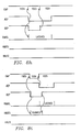
- FIGS 8a-8j there are illustrated timing diagrams showing various operations wherein a Write operation and a Read operation occur close in time during the period of setting or resetting the half flag for the almost empty/almost full status.
- the Write input control signal is represented as a negative going pulse and the Read input control signal is also represented by a negative going pulse.
- the AEP pulse is a normally high signal which is triggered low in response to generation of the falling edge of the Write control signal width.
- This negative going pulse has a predetermined pulse width previously disclosed in Figure 4.
- the AEP negative going pulse is illustrated as occurring simultaneously with the edge of the Write pulse, it is actually delayed therefrom, as will be described hereinbelow.
- the BEP signal is a normally high signal which has a negative going pulse generated off of the rising edge of the Read pulse and is delayed therefrom.
- the BEP negative going pulse has a pulse width that is less than the pulse width of the AEP pulse, as will be described hereinbelow.
- the CMP signal output by NAND gate 186 is normally high for all difference values of the two counters 44 and 46, except for the value 1024.
- the CMP signal is low.
- the half flag HALFZ remains high, but the difference value is incremented for each Write operation. This difference value is the result of counter 44 being incremented and counter 46 not being incremented.
- the initial difference value is 1022 until the first Write operation, wherein the counter is incremented to a value of 1023 on the falling edge of Write.
- the difference value is incremented to 1024 and CMP goes low.
- HALFZ goes low.
- HALFZ will remain low until a Read operation is performed.
- the difference value is decremented from 1025 to 1024. This also results in CMP going low and HALFZ going high.
- the difference value is again decremented to 1023 and the CMP signal goes high.
- Figure 8c illustrates the case where CMP is initially set low as a result of a difference value of 1024 being present. This can be the result of either a Read operation resetting the half flag or a Write operation changing the difference value from 1023 to 1024.
- Figure 8c illustrates the case where a Write operation occurs before a Read operation and there is no overlapping.
- BEP The falling edge of BEP coincides with the change in the difference value from 1025 to 1024, which causes CMP to go low.
- HMATL goes low when AEP goes high and while CMP is high, since latch 192 again becomes transparent. This value is maintained low during BEP, since the output of NOR gate 188 is low and the latch 192 is forced to a low logic state by BEP as a result of pulling down the input to the internal latch 226 in latch 192.
- HMATU goes high, resulting in the flag HALFZ going high for a reset operation.
- the first is setting the flag and the second is resetting the flag.
- the operation of setting the flag is performed by determining that the count value has changed from 1024 to 1025. Therefore, some transition must be examined in order to determine this change. The decision is made by the fact that when AEP falls, it is known that the count value has been incremented since this coincides with the Write operation. Therefore, it is only necessary to know both that the previous count value was 1024 and that the falling edge of AEP has occurred. This would coincide with the count value being incremented to 1025. Therefore, the logic circuitry does not examine a change in CMP but, rather, it examines whether CMP was low, corresponding to a value of 1024, prior to AEP going low. Therefore, the set occurs on the falling edge of AEP.
- AEP prevents any operation related to CMP from being transferred through the circuitry to HMATL and, as such, AEP prevents these glitches from causing inadvertent resets. This is important when considering the occurrence of AEP when the count value is much less than 1024 wherein the half flag would not be set. If a glitch occurred in CMP which would appear as a transition from 1024 to 1025, the glitch would be blanked.
- the only condition that would result in a set operation is the existence of a low on the comparator output CMP or the occurrence of the low going edge of AEP. Therefore, the set operation is isolated from any glitches that occur as a result of the comparator operation and the operation of the counters. The decision is based solely upon the occurrence of the falling edge of AEP and the previous existence of the difference value 1024.
- the operation for setting the flag is to be compared with the operation of resetting the flag.
- resetting the flag it is necessary to examine the transition of CMP to determine that it changed from a value of 1025 to a value of 1024. However, this transition is not examined until the end of BEP.
- any inadvertent glitches will have occurred and the counter settled to the correct value. For example, if the difference value varied from 1027 to 1026 during the Read operation, any glitches that would occur would occur around this transition.
- BEP blanks any potential reset operation until the rising edge thereof. This provides a predetermined amount of time for the counters to settle. Therefore, the reset operation is a function of the half-flag being set, the occurrence of the falling edge of CMP and the fact that the difference value corresponding to the CMP signal is equal to 1024 on the rising edge of BEP.
- Figure 8d illustrates the case where the falling edge of AEP occurs just prior to the falling edge of BEP.
- AEP goes low during a difference of 1024
- CMP goes high since the difference is incremented to 1025.
- HMATL is latched in a high condition.
- the rising edge of CMP causes HMATU to go low and the falling edge of AEP causes HALFZ to go low. This effectively sets the flag.
- the difference value is decremented from 1025 to 1024, causing CMP to go low.
- the period in which CMP is high can be very short.
- HMATU remains low since BEP blanks HMATU and keeps it low until BEP goes back high on the rising edge thereof.
- Figure 8e illustrates the case where the falling edge of BEP occurs just prior to the falling edge of AEP and the difference value is 1024. This indicates the situation where the flag is in a reset state and the difference value changes from 1024 to 1023. Therefore, at the falling edge of BEP, CMP goes high indicating a difference value of 1023. Simultaneously, HMATL goes low since BEP forces the output thereof to a low state. In addition, HMATU also goes low since, as described above, BEP provides a blanking function to present reset during the time that BEP is low.
- Figure 8f describes the case where the falling edges of AEP and BEP occur simultaneously, and the difference value prior to the occurrence of these falling edges is 1024. At the falling edge of AEP and the falling edge of BEP, the difference value will still be 1024. Therefore, CMP remains low both prior to and after the falling edges thereof. Since BEP goes low, the value of HMATL is forced to a low and this low state is latched in the latch 192. Further, HMATU is also forced to a low on the falling edge of BEP. Therefore, the flag stays in the reset state at a logic high. The only way that the flag could be reset to a low state is if the falling edge of AEP occurred just prior to the falling edge of BEP and the high logic state was latched onto HMATL. However, if this did occur, the flag would be reset at the end of AEP, as illustrated in Figure 8d.
- the timing diagram of Figure 8g illustrates the case where the falling edge of AEP occurs simultaneous with the rising edge of BEP, where the difference value was 1024 prior to the falling edge of BEP.
- BEP goes low
- the difference value changes to 1023 and CMP goes high.
- HMATL is forced low and HMATU is forced low.
- the falling edge of AEP causes CMP to go low, since the difference value is now 1024.
- the rising edge of BEP occurs concurrently, and the combination of CMP low and BEP high causes HMATU to go high.
- the falling edge of AEP also latches the low state previously on HMATL for the duration of AEP. HMATL goes high on the rising edge of AEP. Therefore, the flag is not set to a low logic state.
- Figures 8h-8j illustrate the condition wherein the flag is initially set low indicating an almost full state and a Read and a Write operation occur in close proximity.
- Figure 8h illustrates the case where AEP occurs just prior to BEP. Initially, the difference value is 1025 and this difference value changes to 1026 on the falling edge of AEP. HMATL is low when the difference value is 1025 and this value is latched in latch 192 on the falling edge of AEP. When the falling edge of BEP occurs, the difference value changes to 1025 but CMP remains high. Therefore, nothing occurs to change the state of HMATL or HMATU which always remain low and, therefore, the half flag can never be reset.
- the half flag is reset after occurrence of the rising edge of AEP and if HMATU is high at that time. Since CMP never goes low, HMATU will always remain low. The only way for HMATU to go low is for the falling edge of BEP to occur just prior to the falling edge of AEP.
- Figure 8i illustrates the case where the falling edge of BEP occurs just prior to the falling edge of AEP.
- the difference value changes from 1025 to 1024 and CMP goes low.
- HMATU is forced low since BEP goes low, which, as described above, is a portion of the blanking function of the BEP pulse.
- the difference value changes from 1024 to 1025 and HMATL is latched to a low condition.
- the reason that HMATL is latched to a low condition is that BEP forced HMATL to a low during the time in which BEP is low. Since the falling edge of AEP occurs before the rising edge of BEP, the half flag cannot be reset.
- Figure 8j illustrates the case where the falling edge of AEP occurs simultaneous with the rising edge of BEP when the half flag is set low, indicating an almost full condition.
- the falling edge of BEP changes the difference value from 1025 to 1024 and CMP goes low.
- HMATU is forced to a low as a result of the blanking function of BEP until the rising edge thereof.
- HMATL is forced low from the falling edge of BEP until the rising edge thereof. This results in AEP latching the low state onto HMATL on the rising edge thereof, which also causes CMP to go high and also prevents resetting of the flags since the flag cannot be reset during AEP.
- HMATU would go high and reset the flag. However, as soon as the rising edge of AEP occurred, a logic high would be latched into HMATL and the flag would be reset. It is important for this operation that both HMATU be low and that AEP blank the reset function.
- the setting/resetting of the flag occurs when a difference value between the pointers changes from a first predetermined value to the next and second predetermined value.
- This can be an increase in value or a decrease in value.
- the flag is set when it is determined that there has been an increase from the first value, and the flag is reset when it is determined that there has been a decrease to the first value.
- An increase in value from the initial value is determined by first making the decision that the first value is present and then making a determination that there has been an increase. This is done with the use of AEP where AEP in and of itself indicates an increase in value and the only information that is required to set the flag is whether the first value was present prior to the occurrence of the leading edge of AEP.
- AEP blanks out any possible reset operation and any glitches due to the operation of the comparator. Since a comparator transition could occur every time AEP is generated or every time a Write operation occurs, AEP provides this blanking function every time the difference value is incremented.
- the reset operation occurs whenever there is a decrease in the difference value from the second value to the first value and this decision is made in that a reset operation occurs by the mere existence of the first value.
- the first value which in the preferred embodiment is 1024, is present for a much longer duration of time, i.e.
- the reset operation does provide a blanking operation that both stops any reset operation that was previously occurring and also provides a predetermined amount of delay to insure that the counters and the comparator have settled before making this decision.
- the blanking function of BEP in the circuit of Figure 6 illustrates the timing relationship between the reset and set operations.
- AEP blanks any possible occurrence of reset to determine if HMATL is high. For example, during this period, any operation with respect to the comparator and BEP is blanked to prevent a potential high-going glitch from turning on transistor 218.
- AEP has a pulse width that is slightly longer than BEP. This is such that the pulse width of AEP corresponds to the duration of time that HMATU would be blanked by BEP.
- this blanking operation has three invertors 190, 202 and a NOR gate 188 introduced into the chain and AEP is input directly to NAND gate 214, the NOR gate 154 and three invertors 164 compensate for this delay. However, it is important to insure that the reset operation is blanked for the full duration of AEP and that HMATU does not cause a reset operation to occur.
- BEP is operable to blank the reset operation by blanking HMATU during BEP and also to stop any ongoing reset operation.
Landscapes
- Engineering & Computer Science (AREA)
- Theoretical Computer Science (AREA)
- Physics & Mathematics (AREA)
- General Engineering & Computer Science (AREA)
- General Physics & Mathematics (AREA)
- Dram (AREA)
- Communication Control (AREA)
- Synchronisation In Digital Transmission Systems (AREA)
- Dc Digital Transmission (AREA)
- Static Random-Access Memory (AREA)
Applications Claiming Priority (2)
| Application Number | Priority Date | Filing Date | Title |
|---|---|---|---|
| US19155588A | 1988-05-09 | 1988-05-09 | |
| US191555 | 1988-05-09 |
Publications (3)
| Publication Number | Publication Date |
|---|---|
| EP0342107A2 true EP0342107A2 (de) | 1989-11-15 |
| EP0342107A3 EP0342107A3 (de) | 1991-08-21 |
| EP0342107B1 EP0342107B1 (de) | 1996-07-17 |
Family
ID=22705951
Family Applications (1)
| Application Number | Title | Priority Date | Filing Date |
|---|---|---|---|
| EP89401270A Expired - Lifetime EP0342107B1 (de) | 1988-05-09 | 1989-05-05 | Flagge für einen FIFO |
Country Status (4)
| Country | Link |
|---|---|
| EP (1) | EP0342107B1 (de) |
| JP (1) | JP2863545B2 (de) |
| KR (1) | KR0137771B1 (de) |
| DE (1) | DE68926833T2 (de) |
Cited By (7)
| Publication number | Priority date | Publication date | Assignee | Title |
|---|---|---|---|---|
| EP0453110A2 (de) * | 1990-04-20 | 1991-10-23 | British Broadcasting Corporation | Synchronisation von digitalen Audiosignalen |
| EP0481751A2 (de) * | 1990-10-18 | 1992-04-22 | STMicroelectronics, Inc. | Pipelineschaltung zum Vergleich der relativen Differenz zwischen zwei asynchronen Zeigern und einem programmierbaren Wert |
| EP0651319A1 (de) * | 1993-10-29 | 1995-05-03 | AT&T GLOBAL INFORMATION SOLUTIONS INTERNATIONAL INC. | System für Datentransfer |
| CN1078720C (zh) * | 1995-11-04 | 2002-01-30 | 三星电子株式会社 | 输入/输出数据的规模相异的先入先出存贮器及其方法 |
| WO2003065215A2 (en) * | 2002-01-29 | 2003-08-07 | INTEL CORPORATION (a Delawere Corporation) (a corporation of Delaware) | Queue management |
| WO2005098634A2 (en) | 2004-04-01 | 2005-10-20 | Nvidia Corporation | Deadlock avoidance in a bus fabric |
| CN108833300A (zh) * | 2018-06-21 | 2018-11-16 | 厦门大学 | 一种基于单天线的大数据包远距离传输方法 |
Families Citing this family (2)
| Publication number | Priority date | Publication date | Assignee | Title |
|---|---|---|---|---|
| JPH0417187A (ja) * | 1990-05-09 | 1992-01-21 | Nippon Telegr & Teleph Corp <Ntt> | Fifo回路 |
| JP2604482B2 (ja) * | 1990-05-16 | 1997-04-30 | 日本電気通信システム株式会社 | Fifoレジスタ |
Citations (3)
| Publication number | Priority date | Publication date | Assignee | Title |
|---|---|---|---|---|
| US4208713A (en) * | 1977-03-01 | 1980-06-17 | Telefonaktiebolaget L M Ericsson | Address and break signal generator |
| US4486854A (en) * | 1981-10-15 | 1984-12-04 | Codex Corporation | First-in, first-out memory system |
| US4694426A (en) * | 1985-12-20 | 1987-09-15 | Ncr Corporation | Asynchronous FIFO status circuit |
Family Cites Families (1)
| Publication number | Priority date | Publication date | Assignee | Title |
|---|---|---|---|---|
| JPH01234928A (ja) * | 1988-03-16 | 1989-09-20 | Fujitsu Ltd | バッファの状態検出回路 |
-
1989
- 1989-05-05 EP EP89401270A patent/EP0342107B1/de not_active Expired - Lifetime
- 1989-05-05 DE DE68926833T patent/DE68926833T2/de not_active Expired - Fee Related
- 1989-05-09 JP JP1115946A patent/JP2863545B2/ja not_active Expired - Fee Related
- 1989-05-09 KR KR1019890006256A patent/KR0137771B1/ko not_active IP Right Cessation
Patent Citations (3)
| Publication number | Priority date | Publication date | Assignee | Title |
|---|---|---|---|---|
| US4208713A (en) * | 1977-03-01 | 1980-06-17 | Telefonaktiebolaget L M Ericsson | Address and break signal generator |
| US4486854A (en) * | 1981-10-15 | 1984-12-04 | Codex Corporation | First-in, first-out memory system |
| US4694426A (en) * | 1985-12-20 | 1987-09-15 | Ncr Corporation | Asynchronous FIFO status circuit |
Cited By (19)
| Publication number | Priority date | Publication date | Assignee | Title |
|---|---|---|---|---|
| EP0453110A3 (en) * | 1990-04-20 | 1992-08-19 | British Broadcasting Corporation | Synchronisation of digital audio signals |
| EP0453110A2 (de) * | 1990-04-20 | 1991-10-23 | British Broadcasting Corporation | Synchronisation von digitalen Audiosignalen |
| EP0481751A2 (de) * | 1990-10-18 | 1992-04-22 | STMicroelectronics, Inc. | Pipelineschaltung zum Vergleich der relativen Differenz zwischen zwei asynchronen Zeigern und einem programmierbaren Wert |
| EP0481751A3 (en) * | 1990-10-18 | 1993-02-24 | Sgs-Thomson Microelectronics, Inc. | Pipeline circuitry for allowing the comparison of the relative difference between two asynchronous pointers and a programmable value |
| EP0651319A1 (de) * | 1993-10-29 | 1995-05-03 | AT&T GLOBAL INFORMATION SOLUTIONS INTERNATIONAL INC. | System für Datentransfer |
| CN1078720C (zh) * | 1995-11-04 | 2002-01-30 | 三星电子株式会社 | 输入/输出数据的规模相异的先入先出存贮器及其方法 |
| US6993602B2 (en) * | 2002-01-29 | 2006-01-31 | Intel Corporation | Configuring queues based on a given parameter |
| WO2003065215A2 (en) * | 2002-01-29 | 2003-08-07 | INTEL CORPORATION (a Delawere Corporation) (a corporation of Delaware) | Queue management |
| WO2003065215A3 (en) * | 2002-01-29 | 2004-02-26 | Intel Corp A Delawere Corp | Queue management |
| WO2005098634A2 (en) | 2004-04-01 | 2005-10-20 | Nvidia Corporation | Deadlock avoidance in a bus fabric |
| EP1730644A2 (de) * | 2004-04-01 | 2006-12-13 | Nvidia Corporation | Stillstandsvermeidung in einem busfeld |
| EP1730644A4 (de) * | 2004-04-01 | 2007-10-17 | Nvidia Corp | Stillstandsvermeidung in einem busfeld |
| US7418537B2 (en) | 2004-04-01 | 2008-08-26 | Nvidia Corporation | Deadlock avoidance in a bus fabric |
| US7478189B2 (en) | 2004-04-01 | 2009-01-13 | Nvidia Corporation | Deadlock avoidance in a bus fabric |
| EP2172847A2 (de) | 2004-04-01 | 2010-04-07 | Nvidia Corporation | Systemblockadeverhinderung in einer Buskonfiguration |
| EP2172847A3 (de) * | 2004-04-01 | 2010-05-19 | Nvidia Corporation | Systemblockadeverhinderung in einer Buskonfiguration |
| US7882296B2 (en) | 2004-04-01 | 2011-02-01 | Nvidia Corporation | Deadlock avoidance in a bus fabric |
| CN108833300A (zh) * | 2018-06-21 | 2018-11-16 | 厦门大学 | 一种基于单天线的大数据包远距离传输方法 |
| CN108833300B (zh) * | 2018-06-21 | 2020-11-27 | 厦门大学 | 一种基于单天线的大数据包远距离传输方法 |
Also Published As
| Publication number | Publication date |
|---|---|
| JP2863545B2 (ja) | 1999-03-03 |
| KR900018824A (ko) | 1990-12-22 |
| EP0342107A3 (de) | 1991-08-21 |
| DE68926833D1 (de) | 1996-08-22 |
| JPH0277836A (ja) | 1990-03-16 |
| EP0342107B1 (de) | 1996-07-17 |
| KR0137771B1 (ko) | 1998-06-15 |
| DE68926833T2 (de) | 1997-02-20 |
Similar Documents
| Publication | Publication Date | Title |
|---|---|---|
| US4891788A (en) | FIFO with almost full/almost empty flag | |
| US5365485A (en) | Fifo with fast retransmit mode | |
| US6259650B1 (en) | Dual port memory control signals with synchronized read and write pointers | |
| US5088061A (en) | Routing independent circuit components | |
| US5079693A (en) | Bidirectional FIFO buffer having reread and rewrite means | |
| US5311475A (en) | High speed full and empty flag generators for first-in first-out memory | |
| US5305253A (en) | Zero fall-through time asynchronous fifo buffer with nonambiguous empty-full resolution | |
| US5267191A (en) | FIFO memory system | |
| US4748588A (en) | Fast data synchronizer | |
| US5384744A (en) | Look ahead flag for FIFO | |
| US4070630A (en) | Data transfer synchronizing circuit | |
| US5274600A (en) | First-in first-out memory | |
| EP0342107A2 (de) | Flagge für einen FIFO | |
| US5495451A (en) | Apparatus for detecting data input/output states of a plurality of first-in first-out memories | |
| EP0481751B1 (de) | Pipelineschaltung und Verfahren zum Vergleich der relativen Differenz zwischen zwei asynchronen Zeigern und einem programmierbaren Wert | |
| US6075833A (en) | Method and apparatus for counting signal transitions | |
| US11532338B1 (en) | Mediating between asynchronous clock domains while preventing false indications of FIFO occupancy | |
| US6157695A (en) | Counter for performing multiple counts and method thereof | |
| US6480912B1 (en) | Method and apparatus for determining the number of empty memory locations in a FIFO memory device | |
| US7154983B2 (en) | Method of operating a first-in first-out (FIFO) circuit | |
| US5963056A (en) | Full and empty flag generator for synchronous FIFOs | |
| EP0434381B1 (de) | Differenzvergleich zwischen zwei asynchronen Zeigern und einem programmierbaren Wert | |
| US5249154A (en) | Data access controller and method | |
| EP0804762B1 (de) | Selbstprüfende asynchrone datenpuffer | |
| US6680990B1 (en) | Elastic integrated circuit |
Legal Events
| Date | Code | Title | Description |
|---|---|---|---|
| PUAI | Public reference made under article 153(3) epc to a published international application that has entered the european phase |
Free format text: ORIGINAL CODE: 0009012 |
|
| AK | Designated contracting states |
Kind code of ref document: A2 Designated state(s): DE FR GB IT |
|
| PUAL | Search report despatched |
Free format text: ORIGINAL CODE: 0009013 |
|
| AK | Designated contracting states |
Kind code of ref document: A3 Designated state(s): DE FR GB IT |
|
| 17P | Request for examination filed |
Effective date: 19920304 |
|
| 17Q | First examination report despatched |
Effective date: 19940725 |
|
| GRAH | Despatch of communication of intention to grant a patent |
Free format text: ORIGINAL CODE: EPIDOS IGRA |
|
| GRAH | Despatch of communication of intention to grant a patent |
Free format text: ORIGINAL CODE: EPIDOS IGRA |
|
| GRAA | (expected) grant |
Free format text: ORIGINAL CODE: 0009210 |
|
| AK | Designated contracting states |
Kind code of ref document: B1 Designated state(s): DE FR GB IT |
|
| REF | Corresponds to: |
Ref document number: 68926833 Country of ref document: DE Date of ref document: 19960822 |
|
| ITF | It: translation for a ep patent filed | ||
| ET | Fr: translation filed | ||
| PLBE | No opposition filed within time limit |
Free format text: ORIGINAL CODE: 0009261 |
|
| STAA | Information on the status of an ep patent application or granted ep patent |
Free format text: STATUS: NO OPPOSITION FILED WITHIN TIME LIMIT |
|
| 26N | No opposition filed | ||
| PGFP | Annual fee paid to national office [announced via postgrant information from national office to epo] |
Ref country code: DE Payment date: 19980511 Year of fee payment: 10 |
|
| PG25 | Lapsed in a contracting state [announced via postgrant information from national office to epo] |
Ref country code: DE Free format text: LAPSE BECAUSE OF NON-PAYMENT OF DUE FEES Effective date: 20000301 |
|
| REG | Reference to a national code |
Ref country code: GB Ref legal event code: IF02 |
|
| PGFP | Annual fee paid to national office [announced via postgrant information from national office to epo] |
Ref country code: FR Payment date: 20030508 Year of fee payment: 15 |
|
| PGFP | Annual fee paid to national office [announced via postgrant information from national office to epo] |
Ref country code: GB Payment date: 20040505 Year of fee payment: 16 |
|
| PG25 | Lapsed in a contracting state [announced via postgrant information from national office to epo] |
Ref country code: FR Free format text: LAPSE BECAUSE OF NON-PAYMENT OF DUE FEES Effective date: 20050131 |
|
| REG | Reference to a national code |
Ref country code: FR Ref legal event code: ST |
|
| PG25 | Lapsed in a contracting state [announced via postgrant information from national office to epo] |
Ref country code: IT Free format text: LAPSE BECAUSE OF NON-PAYMENT OF DUE FEES;WARNING: LAPSES OF ITALIAN PATENTS WITH EFFECTIVE DATE BEFORE 2007 MAY HAVE OCCURRED AT ANY TIME BEFORE 2007. THE CORRECT EFFECTIVE DATE MAY BE DIFFERENT FROM THE ONE RECORDED. Effective date: 20050505 Ref country code: GB Free format text: LAPSE BECAUSE OF NON-PAYMENT OF DUE FEES Effective date: 20050505 |
|
| GBPC | Gb: european patent ceased through non-payment of renewal fee |
Effective date: 20050505 |