EP0342049B1 - Anordnung zur Speisesteuerung von Fahrzeuggeräten - Google Patents
Anordnung zur Speisesteuerung von Fahrzeuggeräten Download PDFInfo
- Publication number
- EP0342049B1 EP0342049B1 EP89304829A EP89304829A EP0342049B1 EP 0342049 B1 EP0342049 B1 EP 0342049B1 EP 89304829 A EP89304829 A EP 89304829A EP 89304829 A EP89304829 A EP 89304829A EP 0342049 B1 EP0342049 B1 EP 0342049B1
- Authority
- EP
- European Patent Office
- Prior art keywords
- resistor
- transistor
- emergency
- terminal
- signal
- Prior art date
- Legal status (The legal status is an assumption and is not a legal conclusion. Google has not performed a legal analysis and makes no representation as to the accuracy of the status listed.)
- Expired - Lifetime
Links
Images

Classifications
-
- H—ELECTRICITY
- H04—ELECTRIC COMMUNICATION TECHNIQUE
- H04W—WIRELESS COMMUNICATION NETWORKS
- H04W52/00—Power management, e.g. Transmission Power Control [TPC] or power classes
- H04W52/02—Power saving arrangements
- H04W52/0209—Power saving arrangements in terminal devices
- H04W52/0251—Power saving arrangements in terminal devices using monitoring of local events, e.g. events related to user activity
- H04W52/0254—Power saving arrangements in terminal devices using monitoring of local events, e.g. events related to user activity detecting a user operation or a tactile contact or a motion of the device
-
- Y—GENERAL TAGGING OF NEW TECHNOLOGICAL DEVELOPMENTS; GENERAL TAGGING OF CROSS-SECTIONAL TECHNOLOGIES SPANNING OVER SEVERAL SECTIONS OF THE IPC; TECHNICAL SUBJECTS COVERED BY FORMER USPC CROSS-REFERENCE ART COLLECTIONS [XRACs] AND DIGESTS
- Y02—TECHNOLOGIES OR APPLICATIONS FOR MITIGATION OR ADAPTATION AGAINST CLIMATE CHANGE
- Y02D—CLIMATE CHANGE MITIGATION TECHNOLOGIES IN INFORMATION AND COMMUNICATION TECHNOLOGIES [ICT], I.E. INFORMATION AND COMMUNICATION TECHNOLOGIES AIMING AT THE REDUCTION OF THEIR OWN ENERGY USE
- Y02D30/00—Reducing energy consumption in communication networks
- Y02D30/70—Reducing energy consumption in communication networks in wireless communication networks
Definitions
- the present invention relates to a power supply control circuit and, more Particularly, to a power supply control circuit for use in vehicle equipment, such as an automobile radio telephone.
- a conventional power supply control circuit for use in an automobile radio telephcne includes a power switch circuit which controls power supply to the telephone.
- the power switch circuit supplies power to the telephone in response not only to the depression of a power switch in the telephone but also to the turning-on of an ignition key, or switch. If the power supply is done in response only to the depression of the power switch, the automobile battery may run out.
- the prior art power supply control circuit is not satisfactory.
- the user must operate at least two switches, i.e., the ignition switch and the power switch before dialing. Thus, he cannot quickly place a call in an emergency situation.
- a power supply control circuit which is capable of turning vehicle equipment on in an emergency situation regardless of the positions of an ignition key and a power switch, and which consumes a minimum of power in a waiting state.
- a power supply control circuit for use in an automobile telephone to which power is supplied in response to a power switch signal and to an ignition voltage.
- the power switch signal is generated by a power switch in a handset of the telephone.
- the ignition voltage is produced by turning on an ignition key.
- the power supply control circuit comprises an emergency switch which manually produces an emergency switch signal.
- An emergency switch monitor circuit monitors the state of the emergency switch and produces an emergency control signal when it receives the emergency switch signal.
- an ignition voltage control circuit produces the ignition voltage regardlees of the condition of the ignition key.
- a power switch control circuit produces the power switch signal regardless of the condition of the power switch.
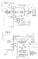
- a mobile telephone 1 is mounted on a vehicle and includes an antenna 10, a transmitter/receiver (TX/RX) section 11 and a handset 12.
- TX/RX section 11 comprises an antenna duplexer 111, a transmitter 112, a receiver 113, a frequency synthesizer 114, and an audio frequency (AF) and control circuit 115.
- the transmitter 112 modulates a radio frequency signal with an AF signal from the AF and control circuit 115 and transmits a modulated radio frequency signal through the antenna duplexer 111 and the antenna 10.
- the receiver 113 receives a radio frequency signal through the antenna duplexer 111 and the antenna 10, demodulates the received radio frequency signal to produce an AF signal and supplies it to the AF and control circuit 115.
- the frequency synthesizer 114 tunes the transmitter 112 and the receiver 113 to one of plural radio channels under the control of the control circuit 115.
- the AF and control circuit 115 exchanges AF signals between the transmitter 112 and the receiver 113, and the handset 12.
- the control circuit 115 interchanges various control signals with a base station (not shown) to control the mobile telephone 1.
- a data bus 117 connects the AF and control circuit 115 and the handset 12.
- the TX/RX section 11 further comprises a power switch circuit 116 which includes a relay 116a and an AND gate 116b.
- the relay 116a is connected with a battery (BTT) terminal 119 which in turn is directly connected with a vehicle battery.
- BTT battery
- An inverted input of AND gate 116b is connected with a power switch 121 through a power switch (PS) terminal 118.
- the other input of AND gate 116b is connected with an ignition key (not shown) through an ignition (IGN) terminal 120. If the ignition key is turned on, an ignition voltage of, for example, 12 volts is applied to IGN terminal 120. In this condition, if the power switch 121 is closed, AND gate 116b produces a high-level signal to cause the relay 116a to be closed. Otherwise, AND gate 116b produces a low-level signal to cause the relay 116a to be open.
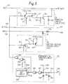
- a mobile radio telephone 100 is mounted on a vehicle having a battery.
- the telephone 100 comprises an emergency power supply control (EPS) circuit 13 which includes a power switch control circuit 131, an ignition voltage control circuit 132, an emergency switch monitor circuit 133, diodes 134 and 135 and an emergency switch 136.
- the emergency switch 136 may be composed of a non-lock type push-button.
- the power switch control circuit 131 is connected with the PS terminal 118, the power switch 121 and the emergency switch monitor circuit 133.
- the ignition voltage control circuit 132 is connected with the anode of diode 135 and the emergency switch monitor circuit 133.
- the cathodes of diodes 134 and 135 are connected with each other and with the IGN terminal 120.
- the anode of diode 134 is connected with the ignition key through a terminal 138.
- the emergency switch 136 is connected between the emergency switch monitor circuit 133 and ground. Power is supplied to the EPS circuit 13 through a terminal 137 with which the vehicle battery and the BTT terminal 119 are connected.
- the emergency switch monitor switch 133 detects the emergency switch signal and thus produces an emergency control signal.
- the emergency control signal is applied to the ignition voltage control circuit 132 and to the power switch control circuit 131.
- the ignition voltage control circuit 132 supplies IGN terminal 120 through the diode 135 with the same voltage as the ignition voltage which is applied to the terminal 138 when the ignition key is turned on.
- the power switch control circuit 131 makes PS terminal 118 be grounded as if the power switch 121 were closed.
- the power switch control circuit 131 includes a PNP transistor 312 whose base, emitter and collector are connected with one end of a resistor 311, a terminal 313 and one end of a resistor 315, respectively. The other end of resistor 315 is grounded.
- the terminal 313 is coupled to five-volt voltage from the vehicle battery through a voltage stabilizer (not shown).
- the collector of transistor 312 is also connected with the base of a PNP transistor 316 through a resistor 314.
- the emitters of transistors 312 and 316 are connected with each other.
- the collector of transistor 316 is connected with the base of an NPN transistor 319.
- the base of transistor 319 is also connected with ground through a resistor 318.
- the emitter of transistor 319 is grounded and the collector of the same is connected with the cathode of a diode 310 and with the power switch 121.
- the anode of diode 310 is grounded.
- the ignition voltage control circuit 132 includes an NPN transistor 323 whose base is connected with one end of a resistor 321 and grounded through a resistor 322.
- the emitter of transistor 323 is grounded and the collector of the same is connected with the base of a PNP transistor 327 through a resistor 324.
- the base and emitter of transistor 327 are connected with each other through a resistor 325.
- the emitter of transistor 327 is also connected with a terminal 326 to which a twelve-volt voltage is applied from the vehicle battery.
- the collector of transistor 327 is connected with the anode of diode 135.
- one end of a resistor 343 is connected with the emergency switch 136.
- the other end of resistor 343 is connected with one end of a resistor 341 and with the cathode of a diode 342.
- the anode of diode 342 is grounded.
- the other end of resistor 341 is connected with one end of a reslstor 339, the inputs of an inverter 337 and one end of a capacitor 340.
- the other end of resistor 339 is connected with a terminal 338 to which a five-volt voltage is applied from the vehicle battery through the voltage stabilizer.
- the other end of capacitor 340 is grounded.
- the output of inverter 337 is connected with the inputs of an inverter 336.
- the output of inverter 336 is connected with the cathode of a diode 335 and one input of a NAND gate 331.
- the anode of diode 335 is connected with a terminal 334b of a: depression detection circuit 334.
- the circuit 334 has another terminal 334a connected with the inputs of an inverter 332 and with one end of a resistor 333. The other end of resistor 333 is grounded.
- the output of inverter 332 is connected with the other input of NAND gate 331.
- the output of NAND gate 311 is connected with the resistors 331 and 321.
- the depression detection circuit 334 may be comprised of a microprocessor.
- a high-voltage signal is applied to the inverter 337 from the terminal 338.
- the inverter 337 outputs a low-level signal and supplies it to the inverter 336 which in turn outputs a high-level signal.
- the high-level signal is applied to the terminal 334b through the diode 335.
- the circuit 334 produces a low-level signal at the terminal 334a (see Fig. 4).
- the circuit 334 (Fig. 3) checks at step S1 whether the level of signal at the terminal 334b is high or low. If high, the circuit 334 causes a level at the terminal 334a to be low at step S3. If low, the circuit 334 causes the level at the terminal 334a to be high at step S2. Steps S2 and S3 return to step S1.
- the low-level signal at the terminal 334a is applied to the inverter 332 which produces a high-level signal and supplies it to one input of NAND gate 331.
- the high-level signal from the inverter 336 is also applied to the other input of NAND gate 331.
- NAND gate 331 produces a low-level signal and supplies it to the power switch control circuit 131 and to the ignition voltage control circuit 132.
- the inverters 336 and 337 are used for impedance matching and the resistor 333 is used for stabilizing the output level of the circuit 334.
- the low-level signal makes the transistor 312 nonconductive, which makes the transistor 316 conductive. This results in cutting off the transistor 319.
- the low-level signal also makes the transistor 323 nonconductive, which makes the transistor 327 nonconductive.
- an emergency switch signal viz., the grounded signal is applied to the inverter 337 through an integrator made up of the resistors 341 and 343 and the capacitor 340, which integrator is inserted to depress the chattering caused by the depression of emergency switch 136.
- the inverter 337 produces a high-level signal to cause the inverter 336 to output a low-level signal.
- the circuit 334 supplies a high-level signal through the terminal 334a to the inverter 332 which in turn supplies a low-level signal to one of inputs of NAND agate 331.
- NAND gate 331 also receives the low-level signal on the other input thereof from the inverter 336 and thus outputs a high-level signal as the emergency control signal.
- the diode 342 prevents a line between the switch 136 and the monitor circuit 133 from storing a negative charge thereon. This line is practically five centimeters in length.
- the transistor 312 turns off, which renders the transistor 316 conductive.
- the transistor 319 is turned on to ground the PS terminal 118 as it would be if power switch 121 is closed.
- the diode 310 has the same function as the diode 342, i.e., preventing a line between the circuit 131 and the PS terminal 118 from storing a negative charge thereon.
- the transistor 323 Responsive to the high-level signal from NAND gate 331, the transistor 323 also turns on, which renders the transistor 327 conductive. As a result, a voltage of 12 volts is applied to the IGN terminal 120 through the diode 135 just as it would be had the ignition key been turned on.
- the emergency switch 136 When the emergency switch 136 is closed, the PS terminal 118 is grounded and the ignition voltage (120) is applied to the IGN terminal 120, irrespective of the states of the power switch 121 and the ignition key. By simply depressing the emergency switch 136, therefore, the user can quickly turn the mobile telephone on to place a call in an emergency situation.
Landscapes
- Engineering & Computer Science (AREA)
- Computer Networks & Wireless Communication (AREA)
- Signal Processing (AREA)
- Stand-By Power Supply Arrangements (AREA)
- Charge And Discharge Circuits For Batteries Or The Like (AREA)
- Mobile Radio Communication Systems (AREA)
Claims (4)
- Elektrisches Fahrzeuggerät, mit Batteriespeiseverbindungen (118) (119) (120), die als Antwort auf eine Zündspannung und ein Leistungsschaltersignal eine Leistung von der Batterie dem Gerät (100) zuführt, einem Leistungsschalter (121) zum manuellen Erzeugen des Leistungsschaltersignals und zu dessen Zufuhr an eine Stromversorgungsverbindung (118), einem Zündschlüssel zum Erzeugen der Zündspannung und zu deren Zufuhr an die Stromversorgungseinrichtung (120), einer Notschaltung (13) mit einer Notschalterüberwachungsschaltung (133) zum Erzeugen eines Notsteuersignals, einer mit dem Leistungsschalter (121) verbundenen und auf das Notsteuersignal ansprechenden Leistungsschaltersteuerschaltung (131) zum Erzeugen des Leistungsschaltersignals und zu dessen Zufuhr an die Stromversorgungsverbindung (118) und einer mit dem Zündschlüssel verbundenen und auf das Notsteuersignal ansprechenden Zündspannungssteuerschaltung (132) zum Erzeugen der Zündspannung und zu deren Zufuhr an die Stromversorgungsverbindung (120) aufweist, wobei(A) die Notschaltung (13) ferner einen Notschalter (136) zum manuellen Erzeugen eines Notschaltersignals aufweist,(B) die Notschalterüberwachungsschaltung (133) einen ersten Widerstand (343), dessen eines Ende mit dem Notschalter (136) verbunden ist, einen zweiten Widerstand (341), dessen eines Ende mit dem anderen Ende des ersten Widerstands (343) verbunden ist, eine erste Diode (342), die zwischen das andere Ende des ersten Widerstands (343) und die Erde geschaltet ist, einen dritten Widerstand (339), der zwischen das andere Ende des zweiten Widerstands (341) und einem mit einer bestimmten Spannung gespeisten Anschluß (338) geschaltet ist, einen Kondensator (340), der zwischen das andere Ende des zweiten Widerstands (341) und die Erde geschaltet ist, einen ersten Inverter (337), dessen Eingang mit dem anderen Ende des zweiten Widerstands (341) verbunden ist, einen zweiten Inverter (336), dessen Eingang mit dem Ausgang des ersten Inverters (337) verbunden ist, eine zweite Diode (335), deren Kathode mit dem Ausgang des zweiten Inverters (336) verbunden ist, einen Druckdetektor (334) mit einem ersten Anschluß (334b) und einem zweiten Anschluß (334a), wobei der erste Anschluß (334a) mit der Anode der zweiten Diode (335) verbunden ist, und der Druckdetektor (334) ein Hochpegelsignal erzeugt, wenn ein Signal an dem ersten Anschluß (334b) niedrig ist, und ein Niederpegelsignal erzeugt, wenn ein Signal an dem ersten Anschluß (334b) hoch ist, und wobei die Hoch- und Niederpegelsignale dem zweiten Anschluß (334a) zugeführt werden, einen vierten Widerstand (333), der zwischen den zweiten Anschluß (334a) und die Erde geschaltet ist, einen dritten Inverter (332), dessen Eingang mit dem zweiten Anschluß (334a) verbunden ist, und eine NICHT-UND-Schaltung (331) besitzt, deren beide Eingänge mit den Ausgängen des zweiten bzw. dritten Inverters (332, 336) verbunden sind und deren Ausgang mit dem Ausgang der Notschalterüberwachungsschaltung (133) verbunden ist, um das Notsteuersignal auszugeben,(C) die Leistungsschaltersteuerschaltung (131) einen fünften Widerstand (311), dessen eines Ende mit dem Ausgang der Notschalterüberwachungsschaltung (133) verbunden ist, und einen ersten Transistor (312), dessen Basis und Emitter mit dem anderen Ende des fünften Widerstands (311) bzw. einem mit einer bestimmten Spannung gespeisten Anschluß (313) verbunden sind, einen sechsten Widerstand (315), der zwischen den Kollektor des ersten Transistors (312) und die Erde geschaltet ist, einen siebten Widerstand (314), dessen eines Ende mit dem Kollektor des ersten Transistors (312) verbunden ist, einen zweiten Transistor (316), dessen Basis und Emitter mit dem anderen Ende des siebten Widerstands (314) bzw. mit dem Emitter des ersten Transistors (312) verbunden sind, und einen achten Widerstand (317), dessen eines Ende mit dem Kollektor des zweiten Transistors (316) verbunden ist, und einen neunten Widerstand (318), der zwischen das andere Ende des siebten Widerstands (317) und die Erde geschaltet ist, und einen dritten Transistor (319), dessen Basis, Emitter und Kollektor mit dem anderen Ende des siebten Widerstands (317), der Erde bzw. dem Ausgang der Leistungsschaltersteuerschaltung (131) verbunden sind, und eine dritte Diode (310) besitzt, deren Anode und Kathode mit der Erde bzw. dem Kollektor des dritten Transistors (319) verbunden sind, und(D) die Zündspannungssteuerschaltung (132) einen zehnten Widerstand (321), dessen eines Ende mit dem Ausgang der Notschalterüberwachungsschaltung (133) verbunden ist, und einen elften Widerstand (322), der zwischen das andere Ende des zehnten Widerstands (321) und die Erde geschaltet ist, und einen vierten Transistor (323), dessen Basis und Emitter mit dem anderen Ende des zehnten Widerstands (321) bzw. der Erde verbunden sind, und einen zwölften Widerstand (324), dessen eines Ende mit dem Kollektor des vierten Transistors (323) verbunden ist, und einen fünften Transistor (327), dessen Basis, Emitter und Kollektor mit dem anderen Ende des zwölften Widerstands (324), dem Ausgang der Zündspannungssteuerschaltung (132) bzw. einem mit einer bestimmten Spannung gespeisten Anschluß (326) verbunden sind, und einen dreizehnten Widerstand (325) aufweist, der zwischen die Basis und den Emitter des fünften Transistors (327) geschaltet ist.
- Elektrisches Fahrzeuggerät nach Anspruch 1, wobei jeder der ersten und zweiten Transistoren (312) (316) PNP-Transistoren sind, und wobei der dritte Transistor (319) ein NPN-Transistor ist.
- Elektrisches Fahrzeuggerät nach Anspruch 1, wobei der erste Transistor (312) ein NPN-Transistor ist, und wobei der zweite Transistor (316) ein PNP-Transistor ist.
- Elektrisches Fahrzeuggerät nach Anspruch 1, wobei der Notschalter (136) ein nichtverriegelbarer Tastschalter ist.
Applications Claiming Priority (2)
| Application Number | Priority Date | Filing Date | Title |
|---|---|---|---|
| JP63116622A JP2652952B2 (ja) | 1988-05-13 | 1988-05-13 | 電源投入回路 |
| JP116622/88 | 1988-05-13 |
Publications (3)
| Publication Number | Publication Date |
|---|---|
| EP0342049A2 EP0342049A2 (de) | 1989-11-15 |
| EP0342049A3 EP0342049A3 (de) | 1991-09-18 |
| EP0342049B1 true EP0342049B1 (de) | 1995-09-13 |
Family
ID=14691747
Family Applications (1)
| Application Number | Title | Priority Date | Filing Date |
|---|---|---|---|
| EP89304829A Expired - Lifetime EP0342049B1 (de) | 1988-05-13 | 1989-05-12 | Anordnung zur Speisesteuerung von Fahrzeuggeräten |
Country Status (2)
| Country | Link |
|---|---|
| EP (1) | EP0342049B1 (de) |
| JP (1) | JP2652952B2 (de) |
Families Citing this family (3)
| Publication number | Priority date | Publication date | Assignee | Title |
|---|---|---|---|---|
| GB2255258B (en) * | 1991-04-25 | 1995-03-08 | Technophone Ltd | Radio telephone |
| EP1071262A4 (de) * | 1999-02-22 | 2004-11-17 | Sanyo Electric Co | Im kraftfahrzeug eingebautes telefongerät |
| KR102820557B1 (ko) * | 2019-11-06 | 2025-06-16 | 엘지이노텍 주식회사 | 차량용 비상 구동 회로 및 제어전원 공급장치 |
Family Cites Families (3)
| Publication number | Priority date | Publication date | Assignee | Title |
|---|---|---|---|---|
| JPS58225743A (ja) * | 1982-06-23 | 1983-12-27 | Toshiba Corp | 無線電話装置 |
| US4513446A (en) * | 1983-02-09 | 1985-04-23 | General Electric Company | Control circuit for a radio transceiver |
| JPS6382848A (ja) * | 1986-09-26 | 1988-04-13 | Nissan Motor Co Ltd | 車両用電圧調整装置 |
-
1988
- 1988-05-13 JP JP63116622A patent/JP2652952B2/ja not_active Expired - Lifetime
-
1989
- 1989-05-12 EP EP89304829A patent/EP0342049B1/de not_active Expired - Lifetime
Also Published As
| Publication number | Publication date |
|---|---|
| EP0342049A2 (de) | 1989-11-15 |
| JPH01286742A (ja) | 1989-11-17 |
| JP2652952B2 (ja) | 1997-09-10 |
| EP0342049A3 (de) | 1991-09-18 |
Similar Documents
| Publication | Publication Date | Title |
|---|---|---|
| EP0326413B1 (de) | Tragbares und in einem Fahrzeug befestigtes Funktelefon | |
| US5155428A (en) | Overdischarge and overvoltage protection circuit for a battery in a portable and mobile communication system | |
| US5170491A (en) | Power source switch circuit | |
| US4736404A (en) | Security arrangement for cordless telephone system | |
| EP1275564B1 (de) | Batterieschaltvorrichtung und notwarnsystem mit dieser vorrichtung | |
| US5592169A (en) | Transmitter for vehicle remote control system | |
| EP0776116A2 (de) | Mobilendgerät mit einer verbesserten Verriegelungsfunktion für die Einschalttaste | |
| CA2021066C (en) | Apparatus for controlling a power supply of an electric machine in a vehicle | |
| EP0498398B1 (de) | Mobiles Telefon | |
| EP0370759B1 (de) | Adapter für den Einbau eines tragbaren Telefons in ein Fahrzeug | |
| US6738603B1 (en) | Radio communication apparatus with retractable antenna and its impedance matching method | |
| GB2209637A (en) | Power source control device in car telephone mobile station system | |
| EP0310284B1 (de) | Fahrzeugfernsprechgerät | |
| EP0115966B1 (de) | Steuerschaltung für ein Funk-Sendeempfangsgerät | |
| US4908846A (en) | Mobile telephone terminal having function to perform call clear process | |
| EP0342049A2 (de) | Anordnung zur Speisesteuerung von Fahrzeuggeräten | |
| US6807430B2 (en) | Portable communication device having back-lighting and high key press noise margin | |
| US5825160A (en) | Power control circuit in wireless mobile communication system | |
| US20050221871A1 (en) | Circuit and method for saving power of a mobile communication terminal | |
| JP3019940B2 (ja) | コードレス通信機の停電検出回路 | |
| JP2864637B2 (ja) | 車載留守番電話装置 | |
| JP2523061B2 (ja) | 無線電話機の電源制御回路 | |
| KR100435555B1 (ko) | 반이중 통신용 송수신기 | |
| JPS61242130A (ja) | バツテリ式通信機 | |
| JPS6253528A (ja) | 車両用通信装置 |
Legal Events
| Date | Code | Title | Description |
|---|---|---|---|
| PUAI | Public reference made under article 153(3) epc to a published international application that has entered the european phase |
Free format text: ORIGINAL CODE: 0009012 |
|
| 17P | Request for examination filed |
Effective date: 19890530 |
|
| AK | Designated contracting states |
Kind code of ref document: A2 Designated state(s): GB SE |
|
| PUAL | Search report despatched |
Free format text: ORIGINAL CODE: 0009013 |
|
| AK | Designated contracting states |
Kind code of ref document: A3 Designated state(s): GB SE |
|
| 17Q | First examination report despatched |
Effective date: 19930628 |
|
| GRAA | (expected) grant |
Free format text: ORIGINAL CODE: 0009210 |
|
| AK | Designated contracting states |
Kind code of ref document: B1 Designated state(s): GB SE |
|
| PLBE | No opposition filed within time limit |
Free format text: ORIGINAL CODE: 0009261 |
|
| STAA | Information on the status of an ep patent application or granted ep patent |
Free format text: STATUS: NO OPPOSITION FILED WITHIN TIME LIMIT |
|
| 26N | No opposition filed | ||
| PGFP | Annual fee paid to national office [announced via postgrant information from national office to epo] |
Ref country code: SE Payment date: 19970506 Year of fee payment: 9 |
|
| PG25 | Lapsed in a contracting state [announced via postgrant information from national office to epo] |
Ref country code: SE Free format text: LAPSE BECAUSE OF NON-PAYMENT OF DUE FEES Effective date: 19980513 |
|
| EUG | Se: european patent has lapsed |
Ref document number: 89304829.8 |
|
| PGFP | Annual fee paid to national office [announced via postgrant information from national office to epo] |
Ref country code: GB Payment date: 20000510 Year of fee payment: 12 |
|
| PG25 | Lapsed in a contracting state [announced via postgrant information from national office to epo] |
Ref country code: GB Free format text: LAPSE BECAUSE OF NON-PAYMENT OF DUE FEES Effective date: 20010512 |
|
| GBPC | Gb: european patent ceased through non-payment of renewal fee |
Effective date: 20010512 |