EP0341806A2 - Appareil pour l'inspection des plaques à cicuits imprimé aux composants montés sur la surface - Google Patents
Appareil pour l'inspection des plaques à cicuits imprimé aux composants montés sur la surface Download PDFInfo
- Publication number
- EP0341806A2 EP0341806A2 EP89301754A EP89301754A EP0341806A2 EP 0341806 A2 EP0341806 A2 EP 0341806A2 EP 89301754 A EP89301754 A EP 89301754A EP 89301754 A EP89301754 A EP 89301754A EP 0341806 A2 EP0341806 A2 EP 0341806A2
- Authority
- EP
- European Patent Office
- Prior art keywords
- printed circuit
- circuit board
- camera
- component
- inspecting
- Prior art date
- Legal status (The legal status is an assumption and is not a legal conclusion. Google has not performed a legal analysis and makes no representation as to the accuracy of the status listed.)
- Granted
Links
Images


Classifications
-
- H—ELECTRICITY
- H05—ELECTRIC TECHNIQUES NOT OTHERWISE PROVIDED FOR
- H05K—PRINTED CIRCUITS; CASINGS OR CONSTRUCTIONAL DETAILS OF ELECTRIC APPARATUS; MANUFACTURE OF ASSEMBLAGES OF ELECTRICAL COMPONENTS
- H05K3/00—Apparatus or processes for manufacturing printed circuits
-
- G—PHYSICS
- G01—MEASURING; TESTING
- G01R—MEASURING ELECTRIC VARIABLES; MEASURING MAGNETIC VARIABLES
- G01R31/00—Arrangements for testing electric properties; Arrangements for locating electric faults; Arrangements for electrical testing characterised by what is being tested not provided for elsewhere
- G01R31/28—Testing of electronic circuits, e.g. by signal tracer
- G01R31/2801—Testing of printed circuits, backplanes, motherboards, hybrid circuits or carriers for multichip packages [MCP]
- G01R31/281—Specific types of tests or tests for a specific type of fault, e.g. thermal mapping, shorts testing
-
- H—ELECTRICITY
- H05—ELECTRIC TECHNIQUES NOT OTHERWISE PROVIDED FOR
- H05K—PRINTED CIRCUITS; CASINGS OR CONSTRUCTIONAL DETAILS OF ELECTRIC APPARATUS; MANUFACTURE OF ASSEMBLAGES OF ELECTRICAL COMPONENTS
- H05K13/00—Apparatus or processes specially adapted for manufacturing or adjusting assemblages of electric components
- H05K13/08—Monitoring manufacture of assemblages
- H05K13/081—Integration of optical monitoring devices in assembly lines; Processes using optical monitoring devices specially adapted for controlling devices or machines in assembly lines
- H05K13/0815—Controlling of component placement on the substrate during or after manufacturing
Definitions
- This invention relates generally to a system for inspecting printed circuit boards, and more particularly, to a system for inspecting printed circuit boards with surface mounted components to verify correct component placement and proper solder connections.
- a printed circuit board is used for mounting and electrically interconnecting electrical components in a predetermined manner.
- this was accomplished using through-the-hole technology which involved the placement of components on the top side of a printed circuit board so that the connecting leads or pins of the components extended through holes (generally plated) provided in the circuit board.
- the leads or pins extending through the circuit board were then bent over to mechanically clamp the electrical components to the printed circuit board, followed by an appropriate soldering operation to complete the necessary connections.
- a mis-insertion which is found prior to soldering is inexpensively repaired, while a mis-insertion which is not found until final assembly (in a product) is often so costly to repair that the assembled board is often discarded rather than attempting to locate and correct the problem.
- Model 5511 A Printed Circuit Board Inspection System which is distributed by the Universal Instruments Corporation of Bingham- ton, New York.
- This apparatus generally employs a series of cameras which are mounted within a fixture (an inspection head) adapted for movement upon an X-Y table to inspect various portions of a printed circuit board (from its underside) which is placed over the X-Y table.
- the inspection head is sequentially advanced to successive viewing fields (typically 2" x 2") established along the surface of the printed circuit board to inspect (through microprocessor analysis) the leads or pins which extend through the printed circuit board, to its bottom, to verify their effective placement based upon a comparison with pre-established norms for the particular printed circuit board which is being tested. Any defects are then reported to the operator, for appropriate correction.
- viewing fields typically 2" x 2
- an inspection head which incorporates a series of four angled, orthogonally placed cameras, each of which is provided with its own corresponding light source (preferably a series of controllable LED's).
- Such structure is provided to enable each viewing field to be inspected from four different perspectives, making sure that a lead or pin which extends from the through-hole is detected in at least one of these four orientations.
- microprocessor controls associated with the apparatus each of a series of anticipated leads or pins can be checked for proper placement in a highly reliable and automated fashion, eliminating the need for tedious visual inspections and the like.
- SMT printed circuit boards incorporate components (both active and passive) which are placed on top of the printed circuit board so that their leads communicate with conductive pads associated with the top face of the printed circuit board. These components are then electrically connected to their associated pads by an appropriate soldering operation, from the top of the board.
- an apparatus which is capable of sequentially monitoring a series of defined viewing fields associated with an SMT printed circuit board, much the same as the automated devices which were used to monitor through-the-hole printed circuit boards, such as the Model 5511A Printed Circuit Board Inspection System.
- an inspection head is mounted to an X-Y table, for directed movement above an SMT printed circuit board which is to be inspected. Both the inspection head, and the X-Y table which supports it, are essentially the same as the corresponding structures of the Model 5511A Printed Circuit Board Inspection System, but are placed in an inverted orientation.
- the inspection head is caused to proceed to successive viewing fields along the surface of the SMT printed circuit board, for inspection by a series of four angled cameras which are orthogonally disposed within the inspection head to inspect each viewing field from four different perspectives.
- Appropriate lighting is provided for use in connection with each of the four cameras to effectively illuminate the viewing field which is being inspected.
- Microprocessor means are provided to control both the lighting which is used to illuminate each viewing field, as well as the cameras associated with the inspection head, and to perform the series of tests which are necessary to verify the integrity of the SMT printed circuit board.
- each of the series of four cameras is sequentially accessed to inspect a particular viewing field from each of four different directions. This is accomplished by selectively acquiring the image which is then being received by the video camera, and converting the acquired image to binary values (for subsequent digital processing) using video conversion techniques which are themselves known to persons of ordinary skill in this art.
- the lighting group which is immediately adjacent to the camera which has been accessed (either a "high” lighting group which is provided near the camera or a “low” lighting group which is provided near the printed circuit board, or both) is used to effectively illuminate the viewing field to obtain the information which is necessary to make these determinations. Defects are appropriately brought to the attention of the operator.
- soldering Following the soldering procedure, it is again necessary to verify that each component remains present on the board, and in its correct orientation, to make sure that the component has not moved between the placement and soldering steps. This is accomplished using the same procedures which were performed prior to soldering. However, following soldering, it is further necessary to verify the integrity of each of the soldering connections associated with the printed circuit board. This includes an inspection of each soldering connection to determine the integrity of the "fillet" which has been produced, and to check for "solder bridges" which may have been produced between adjacent solder connections.
- each of the series of four cameras is again sequentially accessed.
- the lighting which is used in connection with a particular camera is modified so that when a selected camera is accessed, each of two laterally disposed lighting groups which are provided as part of the system are simultaneously activated. This causes illumination of the sides of the solder fillet, which can then be used to make a determination regarding the shape of that fillet.
- steps are taken to again sequentially access each of the four cameras which are provided, in combination with one of the lighting groups (preferably the "high" lighting group) which are located adjacent to the camera, to effectively illuminate a detected solder bridge. In either case, the operator is again advised of any detected defects.
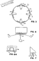
- Fig. 1 shows an apparatus 10 for inspecting printed circuit boards in accordance with the present invention.
- the apparatus 10 generally includes an inspection head 12 which is supported for predetermined movement in a defined plane by an X-Y table which is generally designated as 13, using any of a variety of servo-motor controls which are in themselves known to a person of ordinary skill in this art.
- Both the inspection head 12 and the associated X-Y table 13 are in many ways similar to the inspection head and X-Y table of the Model 5511A Printed Circuit Board Inspection System which is used to inspect through-the-hole printed circuit boards from their bottom.
- the inspection head 12 and the associated X-Y table 13 are mounted in an inverted orientation so that the inspection head 12 is caused to travel across the top of a printed circuit board bearing SMT components, to permit an inspection from above. This is done primarily for convenience since this orientation tends to reduce undesirable movement of the SMT components during the testing (and manufactvring) process.
- the inspection head 12 generally contains both a plurality of TV or video cameras 14, 15, 16, 17, and two series of lighting groups shown at 22, 23, 24, 25 and 26, 27, 28, 29, respectively.
- the cameras and the lighting groups are all contained within a hollow cylinder 30 which is used to house these components in a light-controlled (although not necessarily a light-tight) environment.
- the cameras 14, 15, 16, 17 are orthogonally positioned within the cylinder 30, in general alignment with the moving tables of the X-Y table 13. This is done to place the cameras 14, 15, 16, 17 in normal alignment (which is preferred) with the anticipated components of a printed circuit board to be tested, which are also traditionally (although not always) orthogonally located upon the printed circuit board.
- the video cameras 14, 15, 16, 17 are arranged conically and disposed off of the vertical axis, projecting downwardly toward an open bottom 31 in the cylinder 30. Such positioning is preferred due to the discovery that this orientation enhances the probability of capturing reflected light from structure on the printed circuit board, while minimizing undesirable reflections (back scattered signals) from the printed circuit board itself.
- the angle at which the cameras are caused to deviate from the vertical axis of the inspection head 12 may lie in a range of from 30 to 45 degrees, with an angle of 30 degrees being particularly preferred in this regard.
- a viewing field measuring 1 " x 1 " is preferable to achieve the resolution which is needed for proper determinations to be made in accordance with the present invention. This is preferably accomplished using camera lenses (and extension rings) having a focal length of from 16 to 25 mm.
- the inspection head 12 is caused to proceed between successive viewing fields defined along the surface of the printed circuit board which is being inspected, to make determinations regarding the status of each component on the printed circuit board, its alignment with associated copper pads of the printed circuit board, and the integrity of any solder connections which have been made, as follows.
- steps are then taken to advise the operator of the apparatus 10 of the defect, and its location, to facilitate correction of the problem.
- LED's High speed, high intensity, light emitting diodes
- Such control may include not only a selective activation of LED's, as will be described more fully below, but also a variable adjustment of the intensity of the LED's which have been selected for activation. Controlling the intensity of the lighting which has been selected allows features of a printed circuit board to be more fully developed, enhancing the contrast between the printed circuit board and the components and component features which it contains.
- the illumination which will be used in connection with that camera will be the nearest adjacent lighting group which is positioned closest to the printed circuit board.
- the lighting group 22 would preferably be used.
- the lighting group 23 would preferably be used, and so forth.
- the acquired data is then assembled and compared with a master file which represents a valid (correctly assembled) printed circuit board construction. This is accomplished by defining a plurality of "windows" within a particular viewing field which correspond to the expected locations of the scheduled components, and their attachment leads or pins. Detected reflections are then compared with these pre-established norms to determine whether a particular component feature (side, edge, etc.) lies within its anticipated window, as well as to determine whether the component's connecting leads or pins lie within their anticipated windows. This is generally accomplished by determining the amount of reflected light which is detected within a particular window, and whether the detected amount of reflected light meets a prescribed threshold.
- the placement is deemed correct. If not, a defect is indicated. This can also be accomplished by comparing the location of the component feature, or connecting lead or pin, with the location of the window, and then determining whether these locations are within a prescribed tolerance, if desired.
- any of a number of different components may be located on a given printed circuit board. However, it is traditional that these components will lie in a transverse or longitudinal origination on the printed circuit board. Accordingly, the ends of these components, and their connecting leads or pins, should be capable of being detected by at least one of the four orthogonally disposed cameras which are provided in the inspection head 12. However, it will be understood that all camera angles ' will not always be necessary to determine the proper placement of a particular component, or its connections, depending upon the component's configuration. Accordingly, to reduce data processing times, it is preferred that while all four camera angles will be viewed (acquired), only necessary camera angles (acquisitions) will be processed to make the determinations which are necessary. This can be pre- programed either based upon a known (correct) board configuration, or using a library associated with the apparatus 10 which contains (and defines) the necessary configurations which are to be monitored.
- the apparatus 10 operates to sequentially check each of the components which are to be located within a particular viewing field, as previously described, as the inspection head 12 is moved from the subject viewing field to an adjacent viewing field.
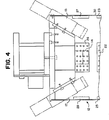
- Fig. 5 of the drawings shows a component 35 which is affixed to a printed circuit board 36 so that the connecting leads 37 are in alignment with their respective connecting pads, shown at 38.
- the camera 14 has been accessed, in combination with the lighting group 22 (as is generally preferred).
- Placement of the edge 39 of the component 35, and accordingly of the component itself, can be detected by monitoring contrasts between the levels of light which are associated with the end 39 of the component 35 (resulting from differentials in brightness, color, surface texture and reflectivity, etc.) and the levels of light which are associated with surrounding structures such as the surface of the printed circuit board 36.
- Placement of the lead 37 can be detected by monitoring projected light (arrow 41) which is reflected back upon the camera 14 (arrow 42).
- this reflection takes advantage of, and results from a "corner effect" wherein light is reflected from the edge 43 of the lead 37 which is itself reflected from the surface of the connecting pad 38. This is permitted by the tinned surfaces of the connecting pad 38 and the edge 43, providing a significant amount of reflected light for use in detecting the placement of component connections.
- Similar data is sequentially acquired by the cameras 15, 16, 17 concerning each component feature, lead and/or pin which has been prescribed for testing by the system, for subsequent processing as previously described.
- steps are preferably taken to accommodate specifics regarding the configuration of a particular printed circuit board.
- this relates to the manner in which lighting is applied to the printed circuit board to properly expose the components which it contains for the optimum delivery of information to the receiving camera.
- it is generally preferred to make use of the lower series of lighting groups 22, 23, 24, 25, since this has been found to generally provide the best contrast between the component and the printed circuit board.
- this may tend to cast shadows from an adjacent component (such as the component 44 shown in phantom) to the component which is being inspected (the component 35) which can limit the ability to detect adjacent circuit components or component connections.
- steps can be taken to cause the higher lighting groups 26, 27, 28, 29 to activate, either in place of or in conjunction with the lighting groups 22. 23, 24, 25, to effectively expose the components on the printed circuit board.
- the lighting group 26 could be used in place of the lighting group 22 (or in combination) to effectively illuminate the end 39 of the component 35, and to provide incident light (arrow 45) for reflection from the end 43 of the connecting lead 37 (arrow 46).
- Steps can also be taken to vary the intensity of the lighting which is applied, to further develop these various features as previously described. Generally, this determination will be an empirical, operator-controlled function which will become apparent when board testing commences, and a particular trend develops.
- a different lighting sequence is preferably used. Rather than activating one of the nearest adjacent lighting groups (either the higher or lower group), steps are taken to simultaneously activate transversely disposed lighting groups positioned on either side of a particular camera. For example, referring to Fig. 6 of the drawings, in accessing the camera 14 steps would be taken to simultaneously activate the lighting groups 23, 25, the lighting groups 27, 29, or a combination of these lighting groups.
- the same lighting groups would be activated when accessing the camera 16. In accessing the cameras 15, 17, steps would be taken to simultaneously activate the lighting groups 22, 24, the lighting groups 26, 28, or a combination of these lighting groups, as desired. This tends to produce a reflected pattern within a particular window such as is illustrated in Fig. 6a of the drawings, having a pair of reflections 47, 48 located in a single window 49.
- An analysis is then made of the contrast ratio (i.e. brightness to darkness) within the window 49 to determine whether the desired reflections 47, 48 are present. If the contrast ratio exceeds a prescribed threshold, an effective solder fillet is deemed to exist. If not, a defect is declared and the operator is advised accordingly.
- solder connections it is necessary to inspect the solder connections for solder bridges which improperly connect adjacent leads or pins, or adjacent connecting pads or paths.
- this is done by defining windows (e.g. at 50) in regions where potential solder bridges can form (e.g. between adjacent connections 51 of an active circuit component) and inspecting for reflections resulting from a solder bridge 52 occurring in the prescribed window.
- windows e.g. at 50
- potential solder bridges e.g. between adjacent connections 51 of an active circuit component
- their detection will generally be best accomplished using the higher lighting groups 26, 27, 28, 29, to obtain the best possible reflection off potential solder bridges.
- this test can be performed either during the inspection for the presence or absence of components and their electrical connections, or in. a separate inspection sequence.
Landscapes
- Engineering & Computer Science (AREA)
- Microelectronics & Electronic Packaging (AREA)
- Manufacturing & Machinery (AREA)
- Physics & Mathematics (AREA)
- Computer Hardware Design (AREA)
- General Engineering & Computer Science (AREA)
- Operations Research (AREA)
- General Physics & Mathematics (AREA)
- Investigating Materials By The Use Of Optical Means Adapted For Particular Applications (AREA)
- Electric Connection Of Electric Components To Printed Circuits (AREA)
- Tests Of Electronic Circuits (AREA)
- Supply And Installment Of Electrical Components (AREA)
- Arrangement Of Elements, Cooling, Sealing, Or The Like Of Lighting Devices (AREA)
Applications Claiming Priority (2)
| Application Number | Priority Date | Filing Date | Title |
|---|---|---|---|
| US15977488A | 1988-02-24 | 1988-02-24 | |
| US159774 | 1988-05-02 |
Publications (3)
| Publication Number | Publication Date |
|---|---|
| EP0341806A2 true EP0341806A2 (fr) | 1989-11-15 |
| EP0341806A3 EP0341806A3 (fr) | 1991-03-13 |
| EP0341806B1 EP0341806B1 (fr) | 1996-12-11 |
Family
ID=22573964
Family Applications (1)
| Application Number | Title | Priority Date | Filing Date |
|---|---|---|---|
| EP89301754A Expired - Lifetime EP0341806B1 (fr) | 1988-02-24 | 1989-02-23 | Appareil pour l'inspection des plaques à cicuits imprimé aux composants montés sur la surface |
Country Status (6)
| Country | Link |
|---|---|
| EP (1) | EP0341806B1 (fr) |
| JP (1) | JP2958014B2 (fr) |
| KR (1) | KR890018024A (fr) |
| AT (1) | ATE146334T1 (fr) |
| CA (1) | CA1313913C (fr) |
| DE (1) | DE68927532T2 (fr) |
Cited By (11)
| Publication number | Priority date | Publication date | Assignee | Title |
|---|---|---|---|---|
| US4972093A (en) * | 1987-10-09 | 1990-11-20 | Pressco Inc. | Inspection lighting system |
| US5051825A (en) * | 1989-04-07 | 1991-09-24 | Pressco, Inc. | Dual image video inspection apparatus |
| US5072127A (en) * | 1987-10-09 | 1991-12-10 | Pressco, Inc. | Engineered video inspecting lighting array |
| EP0466562A3 (en) * | 1990-07-04 | 1992-04-15 | Fujitsu Limited | Method and apparatus for measuring three-dimensional configuration of wire-shaped object in a short time |
| WO1992007455A1 (fr) * | 1990-10-15 | 1992-04-30 | Miroslav Tresky | Dispositif pour enlever des composants defectueux de circuits imprimes |
| US5172005A (en) * | 1991-02-20 | 1992-12-15 | Pressco Technology, Inc. | Engineered lighting system for tdi inspection comprising means for controlling lighting elements in accordance with specimen displacement |
| WO1996021343A1 (fr) | 1994-12-30 | 1996-07-11 | Siemens Aktiengesellschaft | Dispositif de reconnaissance de la position des connexions de composants |
| EP0443289B1 (fr) * | 1990-02-23 | 1998-10-28 | Cimflex Teknowledge Corporation | Appareil pour inspecter des plaques de circuit intégré |
| EP0810817A3 (fr) * | 1996-05-30 | 1998-12-30 | Sony Video (M) SDN.BHD. | Systèmes et méthodes de montage |
| ES2229927A1 (es) * | 2003-10-02 | 2005-04-16 | Sony España, S.A. | Procedimiento y equipo para la inspeccion de soldadura de dispositivos de montaje en superficie. |
| CN105572148A (zh) * | 2015-12-14 | 2016-05-11 | 天津华迈科技有限公司 | 一种贴片质检组件 |
Families Citing this family (4)
| Publication number | Priority date | Publication date | Assignee | Title |
|---|---|---|---|---|
| JP3675167B2 (ja) * | 1998-04-08 | 2005-07-27 | 井関農機株式会社 | 収穫作業車の穀物積替判定装置 |
| JP6013172B2 (ja) * | 2012-12-20 | 2016-10-25 | トヨタ自動車株式会社 | 基板検査装置、基板検査方法及び基板検査プログラム |
| CN112823994A (zh) * | 2019-11-20 | 2021-05-21 | 慈溪市达飞淼电子科技有限公司 | 电路板倒置焊锡工艺 |
| DE102022200391A1 (de) | 2022-01-14 | 2023-07-20 | Robert Bosch Gesellschaft mit beschränkter Haftung | Verfahren zur Qualitätsbeurteilung einer stoffschlüssigen Verbindung zwischen zwei Fügepartner |
Family Cites Families (5)
| Publication number | Priority date | Publication date | Assignee | Title |
|---|---|---|---|---|
| JPS57103399A (en) * | 1980-12-18 | 1982-06-26 | Matsushita Electric Industrial Co Ltd | Device for mounting and inspecting leadless electronic part |
| US4650333A (en) * | 1984-04-12 | 1987-03-17 | International Business Machines Corporation | System for measuring and detecting printed circuit wiring defects |
| JPH0617777B2 (ja) * | 1984-06-02 | 1994-03-09 | 大日本スクリーン製造株式会社 | プリント配線板の撮像方法 |
| US4799268A (en) * | 1985-11-12 | 1989-01-17 | Usm Corporation | Lead sense system for component insertion machine |
| EP0301255A1 (fr) * | 1987-07-30 | 1989-02-01 | Siemens Aktiengesellschaft | Reconnaissance de position tridimensionnelle des broches de composants pour insertion automatique |
-
1989
- 1989-02-23 AT AT89301754T patent/ATE146334T1/de not_active IP Right Cessation
- 1989-02-23 DE DE68927532T patent/DE68927532T2/de not_active Expired - Fee Related
- 1989-02-23 EP EP89301754A patent/EP0341806B1/fr not_active Expired - Lifetime
- 1989-02-24 KR KR1019890002169A patent/KR890018024A/ko not_active Withdrawn
- 1989-02-24 CA CA000592114A patent/CA1313913C/fr not_active Expired - Fee Related
- 1989-02-27 JP JP1046405A patent/JP2958014B2/ja not_active Expired - Fee Related
Cited By (15)
| Publication number | Priority date | Publication date | Assignee | Title |
|---|---|---|---|---|
| US4972093A (en) * | 1987-10-09 | 1990-11-20 | Pressco Inc. | Inspection lighting system |
| US5072127A (en) * | 1987-10-09 | 1991-12-10 | Pressco, Inc. | Engineered video inspecting lighting array |
| US5051825A (en) * | 1989-04-07 | 1991-09-24 | Pressco, Inc. | Dual image video inspection apparatus |
| EP0443289B1 (fr) * | 1990-02-23 | 1998-10-28 | Cimflex Teknowledge Corporation | Appareil pour inspecter des plaques de circuit intégré |
| US5243406A (en) * | 1990-07-04 | 1993-09-07 | Fujitsu Limited | Method and apparatus for measuring three-dimensional configuration of wire-shaped object in a short time |
| EP0466562A3 (en) * | 1990-07-04 | 1992-04-15 | Fujitsu Limited | Method and apparatus for measuring three-dimensional configuration of wire-shaped object in a short time |
| WO1992007455A1 (fr) * | 1990-10-15 | 1992-04-30 | Miroslav Tresky | Dispositif pour enlever des composants defectueux de circuits imprimes |
| US5172005A (en) * | 1991-02-20 | 1992-12-15 | Pressco Technology, Inc. | Engineered lighting system for tdi inspection comprising means for controlling lighting elements in accordance with specimen displacement |
| WO1996021343A1 (fr) | 1994-12-30 | 1996-07-11 | Siemens Aktiengesellschaft | Dispositif de reconnaissance de la position des connexions de composants |
| US6017133A (en) * | 1994-12-30 | 2000-01-25 | Siemens Aktiengesellschaft | Device for recognizing the position of the terminals of components |
| EP0810817A3 (fr) * | 1996-05-30 | 1998-12-30 | Sony Video (M) SDN.BHD. | Systèmes et méthodes de montage |
| US6293007B1 (en) | 1996-05-30 | 2001-09-25 | Sony Video (M) Sdn. Bhd. | Mounting system |
| US6317973B1 (en) | 1996-05-30 | 2001-11-20 | Sony Video (M) Sdn.Bhd | Method for discriminating the kind or type of printed circuit board to selectively set the mounting process therefore |
| ES2229927A1 (es) * | 2003-10-02 | 2005-04-16 | Sony España, S.A. | Procedimiento y equipo para la inspeccion de soldadura de dispositivos de montaje en superficie. |
| CN105572148A (zh) * | 2015-12-14 | 2016-05-11 | 天津华迈科技有限公司 | 一种贴片质检组件 |
Also Published As
| Publication number | Publication date |
|---|---|
| EP0341806A3 (fr) | 1991-03-13 |
| ATE146334T1 (de) | 1996-12-15 |
| EP0341806B1 (fr) | 1996-12-11 |
| DE68927532D1 (de) | 1997-01-23 |
| DE68927532T2 (de) | 1997-07-03 |
| JPH0249500A (ja) | 1990-02-19 |
| CA1313913C (fr) | 1993-02-23 |
| KR890018024A (ko) | 1989-12-18 |
| JP2958014B2 (ja) | 1999-10-06 |
Similar Documents
| Publication | Publication Date | Title |
|---|---|---|
| US5245421A (en) | Apparatus for inspecting printed circuit boards with surface mounted components | |
| EP0341806B1 (fr) | Appareil pour l'inspection des plaques à cicuits imprimé aux composants montés sur la surface | |
| KR950002212B1 (ko) | 기판위전자부품의장착불량의검사및수정방법과그장치 | |
| JP3026981B2 (ja) | 潜在的歪曲プリント回路板点検のための補償システム | |
| CA1285661C (fr) | Mesurage visuel automatique du placement de dispositifs ensurface d'un substrat | |
| JPH10300448A (ja) | プリント回路板アセンブリの検査装置及び方法 | |
| US20030025906A1 (en) | Optical inspection of solder joints | |
| US20020167660A1 (en) | Illumination for integrated circuit board inspection | |
| CN110907469A (zh) | 一种使用机器视觉的电路板焊接检测装置 | |
| EP0365874B1 (fr) | Système et méthode d'inspection optique des sondures | |
| JPS61243303A (ja) | 実装基板の外観検査方式 | |
| US6211959B1 (en) | Method of checking for the presence of connection balls | |
| JPH0330812B2 (fr) | ||
| KR0179758B1 (ko) | 인쇄회로기판상의 부품 실장 상태 검사 방법 | |
| JP3162872B2 (ja) | 電子部品の輪郭認識装置及びその輪郭認識方法 | |
| GB2364119A (en) | Circuit board testing | |
| JPH0267949A (ja) | 半田付検査装置 | |
| KR920005935B1 (ko) | 전자부품 조립상태 검사기의 조명방법 | |
| JPH03192800A (ja) | プリント基板の部品実装認識方法 | |
| KR0141154B1 (ko) | 회로기판의 부품장착상태 검사방법 | |
| Brunelle et al. | Line scan vision system | |
| JP2629798B2 (ja) | 基板検査装置 | |
| JP3203857B2 (ja) | 電子部品検査方法 | |
| JPH09178445A (ja) | 電子部品の端子曲がり検査装置 | |
| GB2308185A (en) | Inspecting component solder joints and leads inserted in printed circuit boards |
Legal Events
| Date | Code | Title | Description |
|---|---|---|---|
| PUAI | Public reference made under article 153(3) epc to a published international application that has entered the european phase |
Free format text: ORIGINAL CODE: 0009012 |
|
| AK | Designated contracting states |
Kind code of ref document: A2 Designated state(s): AT BE CH DE ES FR GB GR IT LI LU NL SE |
|
| PUAL | Search report despatched |
Free format text: ORIGINAL CODE: 0009013 |
|
| AK | Designated contracting states |
Kind code of ref document: A3 Designated state(s): AT BE CH DE ES FR GB GR IT LI LU NL SE |
|
| 17P | Request for examination filed |
Effective date: 19910912 |
|
| 17Q | First examination report despatched |
Effective date: 19930217 |
|
| RAP1 | Party data changed (applicant data changed or rights of an application transferred) |
Owner name: CONTROL AUTOMATION, INC. |
|
| GRAA | (expected) grant |
Free format text: ORIGINAL CODE: 0009210 |
|
| AK | Designated contracting states |
Kind code of ref document: B1 Designated state(s): AT BE CH DE ES FR GB GR IT LI LU NL SE |
|
| DX | Miscellaneous (deleted) | ||
| PG25 | Lapsed in a contracting state [announced via postgrant information from national office to epo] |
Ref country code: IT Free format text: LAPSE BECAUSE OF FAILURE TO SUBMIT A TRANSLATION OF THE DESCRIPTION OR TO PAY THE FEE WITHIN THE PRE;WARNING: LAPSES OF ITALIAN PATENTS WITH EFFECTIVE DATE BEFORE 2007 MAY HAVE OCCURRED AT ANY TIME BEFORE 2007. THE CORRECT EFFECTIVE DATE MAY BE DIFFERENT FROM THE ONE RECORDED.SCRIBED TIME-LIMIT Effective date: 19961211 Ref country code: CH Free format text: LAPSE BECAUSE OF FAILURE TO SUBMIT A TRANSLATION OF THE DESCRIPTION OR TO PAY THE FEE WITHIN THE PRESCRIBED TIME-LIMIT Effective date: 19961211 Ref country code: ES Free format text: THE PATENT HAS BEEN ANNULLED BY A DECISION OF A NATIONAL AUTHORITY Effective date: 19961211 Ref country code: NL Free format text: LAPSE BECAUSE OF FAILURE TO SUBMIT A TRANSLATION OF THE DESCRIPTION OR TO PAY THE FEE WITHIN THE PRESCRIBED TIME-LIMIT Effective date: 19961211 Ref country code: LI Free format text: LAPSE BECAUSE OF FAILURE TO SUBMIT A TRANSLATION OF THE DESCRIPTION OR TO PAY THE FEE WITHIN THE PRESCRIBED TIME-LIMIT Effective date: 19961211 Ref country code: GR Free format text: LAPSE BECAUSE OF FAILURE TO SUBMIT A TRANSLATION OF THE DESCRIPTION OR TO PAY THE FEE WITHIN THE PRESCRIBED TIME-LIMIT Effective date: 19961211 Ref country code: BE Effective date: 19961211 Ref country code: AT Effective date: 19961211 |
|
| REF | Corresponds to: |
Ref document number: 146334 Country of ref document: AT Date of ref document: 19961215 Kind code of ref document: T |
|
| REF | Corresponds to: |
Ref document number: 68927532 Country of ref document: DE Date of ref document: 19970123 |
|
| PG25 | Lapsed in a contracting state [announced via postgrant information from national office to epo] |
Ref country code: LU Free format text: LAPSE BECAUSE OF NON-PAYMENT OF DUE FEES Effective date: 19970228 |
|
| PG25 | Lapsed in a contracting state [announced via postgrant information from national office to epo] |
Ref country code: SE Effective date: 19970311 |
|
| ET | Fr: translation filed | ||
| NLV1 | Nl: lapsed or annulled due to failure to fulfill the requirements of art. 29p and 29m of the patents act | ||
| REG | Reference to a national code |
Ref country code: CH Ref legal event code: PL |
|
| PLBE | No opposition filed within time limit |
Free format text: ORIGINAL CODE: 0009261 |
|
| STAA | Information on the status of an ep patent application or granted ep patent |
Free format text: STATUS: NO OPPOSITION FILED WITHIN TIME LIMIT |
|
| 26N | No opposition filed | ||
| REG | Reference to a national code |
Ref country code: GB Ref legal event code: IF02 |
|
| PGFP | Annual fee paid to national office [announced via postgrant information from national office to epo] |
Ref country code: FR Payment date: 20040219 Year of fee payment: 16 |
|
| PGFP | Annual fee paid to national office [announced via postgrant information from national office to epo] |
Ref country code: GB Payment date: 20050216 Year of fee payment: 17 |
|
| PGFP | Annual fee paid to national office [announced via postgrant information from national office to epo] |
Ref country code: DE Payment date: 20050331 Year of fee payment: 17 |
|
| PG25 | Lapsed in a contracting state [announced via postgrant information from national office to epo] |
Ref country code: FR Free format text: LAPSE BECAUSE OF NON-PAYMENT OF DUE FEES Effective date: 20051031 |
|
| REG | Reference to a national code |
Ref country code: FR Ref legal event code: ST Effective date: 20051031 |
|
| PG25 | Lapsed in a contracting state [announced via postgrant information from national office to epo] |
Ref country code: GB Free format text: LAPSE BECAUSE OF NON-PAYMENT OF DUE FEES Effective date: 20060223 |
|
| PG25 | Lapsed in a contracting state [announced via postgrant information from national office to epo] |
Ref country code: DE Free format text: LAPSE BECAUSE OF NON-PAYMENT OF DUE FEES Effective date: 20060901 |
|
| GBPC | Gb: european patent ceased through non-payment of renewal fee |
Effective date: 20060223 |