EP0341017A2 - Sonnenzelle mit niedergeschlagener Siliziumschicht - Google Patents
Sonnenzelle mit niedergeschlagener Siliziumschicht Download PDFInfo
- Publication number
- EP0341017A2 EP0341017A2 EP89304391A EP89304391A EP0341017A2 EP 0341017 A2 EP0341017 A2 EP 0341017A2 EP 89304391 A EP89304391 A EP 89304391A EP 89304391 A EP89304391 A EP 89304391A EP 0341017 A2 EP0341017 A2 EP 0341017A2
- Authority
- EP
- European Patent Office
- Prior art keywords
- solar cell
- substrate
- barrier layer
- layer
- silicon
- Prior art date
- Legal status (The legal status is an assumption and is not a legal conclusion. Google has not performed a legal analysis and makes no representation as to the accuracy of the status listed.)
- Granted
Links
Images
Classifications
-
- H—ELECTRICITY
- H10—SEMICONDUCTOR DEVICES; ELECTRIC SOLID-STATE DEVICES NOT OTHERWISE PROVIDED FOR
- H10F—INORGANIC SEMICONDUCTOR DEVICES SENSITIVE TO INFRARED RADIATION, LIGHT, ELECTROMAGNETIC RADIATION OF SHORTER WAVELENGTH OR CORPUSCULAR RADIATION
- H10F77/00—Constructional details of devices covered by this subclass
- H10F77/20—Electrodes
- H10F77/206—Electrodes for devices having potential barriers
- H10F77/211—Electrodes for devices having potential barriers for photovoltaic cells
- H10F77/215—Geometries of grid contacts
-
- H—ELECTRICITY
- H10—SEMICONDUCTOR DEVICES; ELECTRIC SOLID-STATE DEVICES NOT OTHERWISE PROVIDED FOR
- H10F—INORGANIC SEMICONDUCTOR DEVICES SENSITIVE TO INFRARED RADIATION, LIGHT, ELECTROMAGNETIC RADIATION OF SHORTER WAVELENGTH OR CORPUSCULAR RADIATION
- H10F77/00—Constructional details of devices covered by this subclass
- H10F77/10—Semiconductor bodies
- H10F77/16—Material structures, e.g. crystalline structures, film structures or crystal plane orientations
- H10F77/169—Thin semiconductor films on metallic or insulating substrates
- H10F77/1692—Thin semiconductor films on metallic or insulating substrates the films including only Group IV materials
-
- H—ELECTRICITY
- H10—SEMICONDUCTOR DEVICES; ELECTRIC SOLID-STATE DEVICES NOT OTHERWISE PROVIDED FOR
- H10F—INORGANIC SEMICONDUCTOR DEVICES SENSITIVE TO INFRARED RADIATION, LIGHT, ELECTROMAGNETIC RADIATION OF SHORTER WAVELENGTH OR CORPUSCULAR RADIATION
- H10F77/00—Constructional details of devices covered by this subclass
- H10F77/20—Electrodes
- H10F77/206—Electrodes for devices having potential barriers
- H10F77/211—Electrodes for devices having potential barriers for photovoltaic cells
-
- H—ELECTRICITY
- H10—SEMICONDUCTOR DEVICES; ELECTRIC SOLID-STATE DEVICES NOT OTHERWISE PROVIDED FOR
- H10F—INORGANIC SEMICONDUCTOR DEVICES SENSITIVE TO INFRARED RADIATION, LIGHT, ELECTROMAGNETIC RADIATION OF SHORTER WAVELENGTH OR CORPUSCULAR RADIATION
- H10F77/00—Constructional details of devices covered by this subclass
- H10F77/40—Optical elements or arrangements
- H10F77/42—Optical elements or arrangements directly associated or integrated with photovoltaic cells, e.g. light-reflecting means or light-concentrating means
- H10F77/48—Back surface reflectors [BSR]
-
- Y—GENERAL TAGGING OF NEW TECHNOLOGICAL DEVELOPMENTS; GENERAL TAGGING OF CROSS-SECTIONAL TECHNOLOGIES SPANNING OVER SEVERAL SECTIONS OF THE IPC; TECHNICAL SUBJECTS COVERED BY FORMER USPC CROSS-REFERENCE ART COLLECTIONS [XRACs] AND DIGESTS
- Y02—TECHNOLOGIES OR APPLICATIONS FOR MITIGATION OR ADAPTATION AGAINST CLIMATE CHANGE
- Y02E—REDUCTION OF GREENHOUSE GAS [GHG] EMISSIONS, RELATED TO ENERGY GENERATION, TRANSMISSION OR DISTRIBUTION
- Y02E10/00—Energy generation through renewable energy sources
- Y02E10/50—Photovoltaic [PV] energy
- Y02E10/52—PV systems with concentrators
Definitions
- This invention relates to the field of art of thin-film photovoltaic solar cells for the conversion of sunlight into electricity.
- Photovoltaic solar cells are semiconductor devices which convert sunlight into electricity.
- Solar cells based on crystalline silicon offer the advantage of high performance and stability.
- the principal barrier to expanded utilization of silicon solar cells for electric power generation is the present high cost of the solar cells.
- Thin-film solar cells use thin layers of semiconductor materials that are deposited or grown on low cost substrates.
- improved performance is also predicted as a consequence of the thinners of the silicon.
- the publication describes further enhancement in performance that results from employing optical confinement techniques.
- U.S. patent no. 4,571,488 issued to A. M. Barnett discloses a thin film solar cell formed on various substrate materials and a conducting or semiconducting metallurgical barrier layer between the substrate on the active layers of the solar cell.
- M. G. Mauk et al. in the Conference Record of the 18th IEEE Photovoltaics Specialists Conference (1985) pp. 192-197 describe a solar cell with thin epitaxial silicon active layers on a heavily doped silicon wafer with a thin film of silicon dioxide between the active layers and the substrate.
- U.S. patent no. 4,677,250 to A. M. Barnett et al. discloses solar cells employing polycrystalline thin-film semiconductor active layers deposited on various substrates and an insulator with conductive nucleation sites between the substrate and the active semiconductor layer.
- a photovoltaic solar cell having a polycrystalline thin-film active semiconductor layer is formed over a thermal expansion matched substrate.
- a barrier layer which is selected to: provide for reflection of light; minimize back surface recombination; and prevent contamination of the active semiconductor layer by the substrate.
- the barrier layer includes a multiplicity of contact regions where the active semiconductor is in electrical communication with the conducting plane of the substrate.
- the substrate is a conductive ceramic material comprised of silicon and meltable glass and/or silicon carbide
- the barrier is an insulating material
- the contact regions are openings in the barrier layer exposing less than 5% of substrate and the active semiconductor is a silicon p-n homojunction.
- Desired properties of a polycrystalline thin-film silicon active semiconductor in accordance with the teachings of this invention are: planar film with single crystal grains at least twice as wide as thickness; thickness in the range 5 to 100 microns; benign grain boundaries; minority carrier diffusion length at least two times the thickness; and a substrate to provide mechanical support and back plane conductor.
- the criteria on grain aspect ratio, diffusion length and grain boundaries are applied to minimize recombination losses.
- Optical confinement is also necessary to recapture the loss in light generated current owing to the silicon thinness. Optical confinement accomplishes this by increasing the effective photon absorption length in thin silicon solar cells.
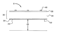
- Shown in the Figure is a schematic cross-section of a solar cell 10 in accordance with the invention.
- This device conforms to the aforementioned design criteria and may be manufactured at low cost.
- the solar cell is formed on substrate 100 which functions as a mechanical support and includes a back plane conductor 110 over which the solar cell is formed.
- the substrate material is selected to have a thermal expansion coefficient that is matched to silicon to minimize stress during the fabrication of the solar cell, which may require processing at temperatures above 1410 o C, the melting point of silicon.
- the thermal expansion coefficient of silicon increases monotonically from 4 to 5 x 10 ⁇ 6 cm/cm- o C in the temperature range 400 to 1000 o C.
- a substrate material in accordance with the teachings of this invention with a thermal expansion coefficient of 4 x 10 ⁇ 6 cm/cm- o C is acceptable.
- the substrate may be electrically conductive or non-conductive, although a conductive substrate is preferred. If the substrate is not conductive, a back plane conductor material (not shown in the Figure), such as a layer of metal, is provided on the surface of the substrate upon which the cell is formed. Optionally a back plane conductor material may also be provided as a separate layer over a conductive substrate, as well.
- the substrate may also be textured to provide the diffuse reflection of light and optical confinement.
- external electrical contact means such as silver, is applied to the bottom of the substrate 100 .
- the preferred substrate in accordance with the teachings of this invention is a ceramic material, that is, a nonmetallic inorganic material containing a high proportion of silicon.
- a ceramic comprised of low purity silicon in the range of 20 to 90% by weight and upto 80% by weight of silicon carbide and/or a glass, has been found to be suitable.
- a conductive ceramic substrate is fabricated from a mixture of 40% by weight silicon powder with initial particle size less than 500 microns and 60% SiC with particle sizes less than 100 microns by means of powder metallurgy techniques, including sintering in an apparatus with an oxygen free chamber which employes a graphite heater designed to provide a suitable thermal profile to accomplish the sintered product.
- the powder mixture is formed into a low density member which is sintered or fused at sufficiently high temperature to form a dense conductive ceramic substrate having an average bulk resistivity of 0.001 to 10.00 ohm-cm, an average density of about 1.5 to 1.9 gram per cubic centimeter, a thickness of 0.03 to 0.08 cm and area that it 10 cm x 10 cm or larger.
- barrier layer 200 Over the back plane conductor of the substrate is barrier layer 200 and active semiconductor 300 is formed over the barrier layer.
- Barrier layer 200 is selected to: provide strength at the temperatures required for fabrication of the cell; act as a barrier to prevent diffusion of impurities from the substrate into the active layer of the solar cell; to passivate the interface between the barrier layer and active semiconductor in order to minimize surface recombination of photo-generated carriers; have an index of refraction that is different from that of the active semiconductor in order to provide a reflective surface for optical confinement.
- Barrier 200 may be a single layer or multiple layers with each layer satisfying one or more of these requirements.
- the multi-layer barrier comprises a first barrier layer of titanium diboride, or titanium dioxide or aluminum oxide over the substrate to provide for strength and act as diffusion barrier.
- a second barrier layer of silicon dioxide which acts to minimize surface recombination and to also provide for reflection, covers the first barrier to form a multi-layer barrier in accordance with the teachings of this invention.
- the titanium diboride may also serve as back plane conductor 110 and as a reflector.
- titanium diboride plus silicon dioxide is preferred.
- the thickness of barrier 200 is 0.1 to 1.0 micron.
- silicon dioxide or silicon nitride may be used, and silicon dioxide is preferred.
- the single silicon dioxide barrier thickness is 0.4 micron.
- Contact regions 210 provide for electrical communication between back contact plane 110 and active semiconductor 300 .
- Contact regions 210 in accordance with the teachings of this invention are a multiplicity of openings in barrier layer 200 .
- the size and spatial distribution of openings is selected such that contact regions 210 occupy 0.5 to 5 % of the area of barrier 200 .
- an array of circular openings of 10 micron diameter spaced apart on 100 micron centers or a series of parallel grooves that are 10 microns wide and 500 microns apart would be suitable.
- Barrier 200 and contact regions 210 can be formed by coating the back contact plane 110 of substrate 100 with the barrier in the desired pattern. Screen printing, spray coating or sputtering through a mask are useful methods of forming the barrier with contact regions according to this invention. Alternately, the barrier layer may be applied as a single continuous layer and the contact regions formed by selective removal of barrier material. Selective removal may be accomplished by a variety of techniques including photolithographic or serigraphic patterning followed by chemical etching, mechanical scribing or jet etching.
- This invention further contemplates forming the contact regions 210 such that the height of barrier 200 above the back contact plane and the height of the contact regions are approximately the same in the order to facilitate application of active semiconductor layer 300 .
- This may be accomplished by selectively filling the openings in the barrier with a suitable material such as conductive ceramic or metal.
- the material should be capable of making ohmic contact to the semiconductor layer and may further serve as a dopant source for formation of a back surface field in the semiconductor.
- barrier layer 200 When the substrate is of sufficient purity, barrier layer 200 may be omitted with some loss in efficiency due to the absence of optical enhancement that is provided by the barrier. An efficiency of 15% is expected when the barrier is omitted.
- Active semiconductor layer 300 is comprised of two contiguous regions of opposite conductivity type and a photovoltaic junction.
- semiconductor layer 300 is a polycrystalline thin-film of silicon between 5 and 100 microns thick and preferably 30 microns thick. The grain diameter of the polycrystalline silicon should be at least twice the film thickness.
- Base region 310 of semiconductor layer 300 is p-type silicon that is 5 to 100 micron thick and is doped to have a p-type carrier concentration of 1 x 10¹⁶ to 5 x 1017 cm ⁇ 3 and is characterized by a minority carrier diffusion length of at least twice the thickness.
- a thin n-type silicon emitter region 320 typically 0.2 micron thick and doped to n-type carrier concentration of 1020 cm ⁇ 3, forms a p-n homojunction with base region 320 .
- a solar cell featuring a polycrystalline silicon thin film semiconductor in accordance with this invention is expected to have conversion efficiency greater than 19%.
- Another feature of the thin solar cell of this invention is that the requirements for minority carrier transport properties are far less severe than for conventional thick silicon cells. For example when the active semiconductor is 30 microns thick, a diffusion length of only 60 microns is all that is required to achieve high performance. Accordingly, great flexibility in the method of forming the active semiconductor is available for adapting low cost manufacturing methods to producing solar cells in accordance with this invention.
- coating techniques which may be used alone or in conjunction with a re-crystallization step following application of the semiconductor material.
- coating methods such as chemical vapor deposition, growth from liquid saturated solution, sputtering, vacuum evaporation, ionized cluster beam deposition, spray coating, plasma arc spraying and powder metallurgy may be used to deposit the active semiconductor.
- Chemical vapor deposition in conjunction with re-crystallization is preferred for forming base region 310 of active semiconductor 300 and diffusion doping is preferred for forming emitter region 310 .
- the solar cell of this invention is completed by transparent contact means 400 such as a metal grid that is applied to the light receiving surface of semiconductor 300 using methods known in the art as screen printing, evaporation and the like.
- Anti-reflection and surface passivation coatings may also be applied in order to increase the performance of a solar cell in accordance with the teachings of this invention.
Landscapes
- Photovoltaic Devices (AREA)
Applications Claiming Priority (2)
| Application Number | Priority Date | Filing Date | Title |
|---|---|---|---|
| US07/190,138 US5057163A (en) | 1988-05-04 | 1988-05-04 | Deposited-silicon film solar cell |
| US190138 | 1998-11-12 |
Publications (3)
| Publication Number | Publication Date |
|---|---|
| EP0341017A2 true EP0341017A2 (de) | 1989-11-08 |
| EP0341017A3 EP0341017A3 (de) | 1990-06-20 |
| EP0341017B1 EP0341017B1 (de) | 1997-02-12 |
Family
ID=22700161
Family Applications (1)
| Application Number | Title | Priority Date | Filing Date |
|---|---|---|---|
| EP89304391A Expired - Lifetime EP0341017B1 (de) | 1988-05-04 | 1989-05-02 | Sonnenzelle mit niedergeschlagener Siliziumschicht |
Country Status (5)
| Country | Link |
|---|---|
| US (1) | US5057163A (de) |
| EP (1) | EP0341017B1 (de) |
| JP (1) | JP2774142B2 (de) |
| DE (1) | DE68927760T2 (de) |
| ES (1) | ES2099068T3 (de) |
Cited By (10)
| Publication number | Priority date | Publication date | Assignee | Title |
|---|---|---|---|---|
| DE19743692A1 (de) * | 1997-10-02 | 1999-04-08 | Zae Bayern | Multifunktionsschicht zur Verbesserung des Wirkungsgrades von kristallinen Dünnschicht Silizium Solarzellen |
| US5963790A (en) * | 1992-07-22 | 1999-10-05 | Mitsubshiki Denki Kabushiki Kaisha | Method of producing thin film solar cell |
| WO2000002259A1 (en) * | 1998-07-03 | 2000-01-13 | Interuniversitair Micro-Elektronica Centrum | A thin-film opto-electronic device and a method of making it |
| WO2000002253A3 (en) * | 1998-07-02 | 2000-07-06 | Astropower | Silicon thin-film, integrated solar cell, module, and methods of manufacturing the same |
| EP0978146A4 (de) * | 1997-03-04 | 2000-08-09 | Astropower Inc | Polykristallines solarzellensubstrat mit säulenförmigen körnern und verbessertes herstellungsverfahren |
| AU2002301188B2 (en) * | 1998-07-02 | 2004-04-29 | Astropower | Silicon thin-film, integrated solar cell, module, and methods of manufacturing the same |
| WO2007040774A1 (en) * | 2005-09-16 | 2007-04-12 | Blue Square Energy Incorporated | Photovoltaic solar cell and method of making the same |
| EP1993142A1 (de) * | 2007-05-14 | 2008-11-19 | Fraunhofer-Gesellschaft zur Förderung der angewandten Forschung e.V. | Reflektiv beschichtetes Halbleiterbauelement, Verfahren zu dessen Herstellung sowie dessen Verwendung |
| FR2971086A1 (fr) * | 2011-01-31 | 2012-08-03 | Inst Polytechnique Grenoble | Structure adaptee a la formation de cellules solaires |
| EP2341546A3 (de) * | 2009-12-29 | 2013-01-09 | Auria Solar Co., Ltd. | Solarzelle und Herstellungsverfahren dafür |
Families Citing this family (95)
| Publication number | Priority date | Publication date | Assignee | Title |
|---|---|---|---|---|
| US5211761A (en) * | 1990-06-29 | 1993-05-18 | Sanyo Electric Co., Ltd. | Photovoltaic device and manufacturing method thereof |
| US5221365A (en) * | 1990-10-22 | 1993-06-22 | Sanyo Electric Co., Ltd. | Photovoltaic cell and method of manufacturing polycrystalline semiconductive film |
| US5273608A (en) * | 1990-11-29 | 1993-12-28 | United Solar Systems Corporation | Method of encapsulating a photovoltaic device |
| US5230746A (en) * | 1992-03-03 | 1993-07-27 | Amoco Corporation | Photovoltaic device having enhanced rear reflecting contact |
| US5266125A (en) * | 1992-05-12 | 1993-11-30 | Astropower, Inc. | Interconnected silicon film solar cell array |
| US5401331A (en) * | 1993-09-07 | 1995-03-28 | Midwest Research Institute | Substrate for thin silicon solar cells |
| JP3478618B2 (ja) * | 1993-11-30 | 2003-12-15 | キヤノン株式会社 | 光電変換素子及びその製造方法 |
| US5626687A (en) * | 1995-03-29 | 1997-05-06 | The United States Of America As Represented By The United States Department Of Energy | Thermophotovoltaic in-situ mirror cell |
| US5977636A (en) * | 1997-01-17 | 1999-11-02 | Micron Technology, Inc. | Method of forming an electrically conductive contact plug, method of forming a reactive or diffusion barrier layer over a substrate, integrated circuitry, and method of forming a layer of titanium boride |
| EP0993052B1 (de) * | 1998-09-28 | 2009-01-14 | Sharp Kabushiki Kaisha | Weltraumsolarzelle |
| US7507903B2 (en) | 1999-03-30 | 2009-03-24 | Daniel Luch | Substrate and collector grid structures for integrated series connected photovoltaic arrays and process of manufacture of such arrays |
| US8664030B2 (en) | 1999-03-30 | 2014-03-04 | Daniel Luch | Collector grid and interconnect structures for photovoltaic arrays and modules |
| US8222513B2 (en) | 2006-04-13 | 2012-07-17 | Daniel Luch | Collector grid, electrode structures and interconnect structures for photovoltaic arrays and methods of manufacture |
| US20090111206A1 (en) | 1999-03-30 | 2009-04-30 | Daniel Luch | Collector grid, electrode structures and interrconnect structures for photovoltaic arrays and methods of manufacture |
| US8138413B2 (en) | 2006-04-13 | 2012-03-20 | Daniel Luch | Collector grid and interconnect structures for photovoltaic arrays and modules |
| US8198696B2 (en) | 2000-02-04 | 2012-06-12 | Daniel Luch | Substrate structures for integrated series connected photovoltaic arrays and process of manufacture of such arrays |
| US7271333B2 (en) * | 2001-07-20 | 2007-09-18 | Ascent Solar Technologies, Inc. | Apparatus and method of production of thin film photovoltaic modules |
| US6781707B2 (en) | 2002-03-22 | 2004-08-24 | Orasee Corp. | Multi-spectral display |
| DE102004033553A1 (de) * | 2004-07-09 | 2006-01-26 | Bayerisches Zentrum für Angewandte Energieforschung e.V. | Halbleiterbauelemente aus dünnem Silizium auf keramischem Trägersubstrat und Verfahren zu dessen Herstellung |
| US7732229B2 (en) | 2004-09-18 | 2010-06-08 | Nanosolar, Inc. | Formation of solar cells with conductive barrier layers and foil substrates |
| US7838868B2 (en) * | 2005-01-20 | 2010-11-23 | Nanosolar, Inc. | Optoelectronic architecture having compound conducting substrate |
| US8927315B1 (en) | 2005-01-20 | 2015-01-06 | Aeris Capital Sustainable Ip Ltd. | High-throughput assembly of series interconnected solar cells |
| US7572334B2 (en) | 2006-01-03 | 2009-08-11 | Applied Materials, Inc. | Apparatus for fabricating large-surface area polycrystalline silicon sheets for solar cell application |
| US8884155B2 (en) | 2006-04-13 | 2014-11-11 | Daniel Luch | Collector grid and interconnect structures for photovoltaic arrays and modules |
| US9006563B2 (en) | 2006-04-13 | 2015-04-14 | Solannex, Inc. | Collector grid and interconnect structures for photovoltaic arrays and modules |
| US8822810B2 (en) | 2006-04-13 | 2014-09-02 | Daniel Luch | Collector grid and interconnect structures for photovoltaic arrays and modules |
| US8729385B2 (en) | 2006-04-13 | 2014-05-20 | Daniel Luch | Collector grid and interconnect structures for photovoltaic arrays and modules |
| US9865758B2 (en) | 2006-04-13 | 2018-01-09 | Daniel Luch | Collector grid and interconnect structures for photovoltaic arrays and modules |
| US9236512B2 (en) | 2006-04-13 | 2016-01-12 | Daniel Luch | Collector grid and interconnect structures for photovoltaic arrays and modules |
| US7959707B2 (en) * | 2006-04-28 | 2011-06-14 | Sri International | Methods for producing consolidated materials |
| WO2008060704A2 (en) * | 2006-06-02 | 2008-05-22 | Innovalight, Inc. | Photoactive materials containing group iv nanostructures and optoelectronic devices made therefrom |
| WO2008030966A1 (en) * | 2006-09-07 | 2008-03-13 | Innovalight, Inc. | Semiconductor thin films formed from group iv nanoparticles |
| US20080092947A1 (en) * | 2006-10-24 | 2008-04-24 | Applied Materials, Inc. | Pulse plating of a low stress film on a solar cell substrate |
| US20080121276A1 (en) * | 2006-11-29 | 2008-05-29 | Applied Materials, Inc. | Selective electroless deposition for solar cells |
| US7736928B2 (en) * | 2006-12-01 | 2010-06-15 | Applied Materials, Inc. | Precision printing electroplating through plating mask on a solar cell substrate |
| US20080128019A1 (en) * | 2006-12-01 | 2008-06-05 | Applied Materials, Inc. | Method of metallizing a solar cell substrate |
| US7704352B2 (en) * | 2006-12-01 | 2010-04-27 | Applied Materials, Inc. | High-aspect ratio anode and apparatus for high-speed electroplating on a solar cell substrate |
| US7799182B2 (en) * | 2006-12-01 | 2010-09-21 | Applied Materials, Inc. | Electroplating on roll-to-roll flexible solar cell substrates |
| US7776724B2 (en) * | 2006-12-07 | 2010-08-17 | Innovalight, Inc. | Methods of filling a set of interstitial spaces of a nanoparticle thin film with a dielectric material |
| CN101647092A (zh) * | 2006-12-13 | 2010-02-10 | 创新发光体公司 | 在ⅳ族半导体基底上形成外延层的方法 |
| US7718707B2 (en) * | 2006-12-21 | 2010-05-18 | Innovalight, Inc. | Method for preparing nanoparticle thin films |
| EP2140483A1 (de) * | 2007-04-04 | 2010-01-06 | Innovalight, Inc. | Verfahren zur optimierung von dünnschichtbildung mit reaktiven gasen |
| WO2008155786A1 (en) * | 2007-06-20 | 2008-12-24 | Cisel S.R.L. - Circuiti Stampati Per Applicazioni Elettroniche | Photovoltaic module and modular panel made with it to collect radiant solar energy and its transformation into electrical energy |
| US8968438B2 (en) * | 2007-07-10 | 2015-03-03 | Innovalight, Inc. | Methods and apparatus for the in situ collection of nucleated particles |
| US8247254B2 (en) * | 2007-07-13 | 2012-08-21 | Silicon China (HK) Ltd. | System and method for forming solar cell structures |
| US20090053878A1 (en) * | 2007-08-21 | 2009-02-26 | Maxim Kelman | Method for fabrication of semiconductor thin films using flash lamp processing |
| US9287430B1 (en) * | 2007-11-01 | 2016-03-15 | Sandia Corporation | Photovoltaic solar concentrator |
| DE102007054384A1 (de) | 2007-11-14 | 2009-05-20 | Institut Für Solarenergieforschung Gmbh | Verfahren zum Herstellen einer Solarzelle mit einer oberflächenpassivierenden Dielektrikumdoppelschicht und entsprechende Solarzelle |
| ES2402779T3 (es) * | 2007-12-14 | 2013-05-08 | Fraunhofer-Gesellschaft zur Förderung der angewandten Forschung e.V. | Célula solar de película delgada y procedimiento para su fabricación |
| US8481845B2 (en) * | 2008-02-05 | 2013-07-09 | Gtat Corporation | Method to form a photovoltaic cell comprising a thin lamina |
| US8129613B2 (en) * | 2008-02-05 | 2012-03-06 | Twin Creeks Technologies, Inc. | Photovoltaic cell comprising a thin lamina having low base resistivity and method of making |
| US8563352B2 (en) * | 2008-02-05 | 2013-10-22 | Gtat Corporation | Creation and translation of low-relief texture for a photovoltaic cell |
| US7851336B2 (en) * | 2008-03-13 | 2010-12-14 | Innovalight, Inc. | Method of forming a passivated densified nanoparticle thin film on a substrate |
| US20090255574A1 (en) * | 2008-04-14 | 2009-10-15 | Sierra Solar Power, Inc. | Solar cell fabricated by silicon liquid-phase deposition |
| US8247312B2 (en) * | 2008-04-24 | 2012-08-21 | Innovalight, Inc. | Methods for printing an ink on a textured wafer surface |
| US8338209B2 (en) * | 2008-08-10 | 2012-12-25 | Twin Creeks Technologies, Inc. | Photovoltaic cell comprising a thin lamina having a rear junction and method of making |
| US20100032010A1 (en) * | 2008-08-10 | 2010-02-11 | Twin Creeks Technologies, Inc. | Method to mitigate shunt formation in a photovoltaic cell comprising a thin lamina |
| US20100031995A1 (en) * | 2008-08-10 | 2010-02-11 | Twin Creeks Technologies, Inc. | Photovoltaic module comprising thin laminae configured to mitigate efficiency loss due to shunt formation |
| US8106293B2 (en) * | 2008-08-14 | 2012-01-31 | Mh Solar Co., Ltd. | Photovoltaic cell with buffer zone |
| US8293079B2 (en) * | 2008-08-28 | 2012-10-23 | Mh Solar Co., Ltd. | Electrolysis via vertical multi-junction photovoltaic cell |
| US20100037937A1 (en) * | 2008-08-15 | 2010-02-18 | Sater Bernard L | Photovoltaic cell with patterned contacts |
| US20100037943A1 (en) * | 2008-08-14 | 2010-02-18 | Sater Bernard L | Vertical multijunction cell with textured surface |
| US20100126849A1 (en) * | 2008-11-24 | 2010-05-27 | Applied Materials, Inc. | Apparatus and method for forming 3d nanostructure electrode for electrochemical battery and capacitor |
| EP2190033A1 (de) | 2008-11-24 | 2010-05-26 | Fraunhofer-Gesellschaft zur Förderung der angewandten Forschung e.V. | Tandemsolarzelle aus kristallinem Silizium und kristallinem Siliziumcarbid sowie Verfahren zu dessen Herstellung |
| US8367924B2 (en) * | 2009-01-27 | 2013-02-05 | Applied Materials, Inc. | Buried insulator isolation for solar cell contacts |
| FR2943848B1 (fr) * | 2009-03-27 | 2012-02-03 | Jean Pierre Medina | Procede et machine de fabrication d'un semi-conducteur, du type cellule photovoltaique ou composant electronique similaire |
| US8247243B2 (en) | 2009-05-22 | 2012-08-21 | Nanosolar, Inc. | Solar cell interconnection |
| US20110272011A1 (en) * | 2009-06-05 | 2011-11-10 | Amberwave, Inc. | Solar Cell |
| US8110419B2 (en) | 2009-08-20 | 2012-02-07 | Integrated Photovoltaic, Inc. | Process of manufacturing photovoltaic device |
| US8476660B2 (en) * | 2009-08-20 | 2013-07-02 | Integrated Photovoltaics, Inc. | Photovoltaic cell on substrate |
| KR20110047861A (ko) * | 2009-10-30 | 2011-05-09 | 삼성전자주식회사 | 태양 전지 및 이의 제조 방법 |
| US9012766B2 (en) * | 2009-11-12 | 2015-04-21 | Silevo, Inc. | Aluminum grid as backside conductor on epitaxial silicon thin film solar cells |
| US8349626B2 (en) * | 2010-03-23 | 2013-01-08 | Gtat Corporation | Creation of low-relief texture for a photovoltaic cell |
| US9214576B2 (en) | 2010-06-09 | 2015-12-15 | Solarcity Corporation | Transparent conducting oxide for photovoltaic devices |
| US9461186B2 (en) | 2010-07-15 | 2016-10-04 | First Solar, Inc. | Back contact for a photovoltaic module |
| US9054256B2 (en) | 2011-06-02 | 2015-06-09 | Solarcity Corporation | Tunneling-junction solar cell with copper grid for concentrated photovoltaic application |
| US20130125983A1 (en) * | 2011-11-18 | 2013-05-23 | Integrated Photovoltaic, Inc. | Imprinted Dielectric Structures |
| EP2805355A4 (de) * | 2012-01-19 | 2015-08-26 | Nuvosun Inc | Schutzbeschichtungen für fotovoltaische zellen |
| US9865754B2 (en) | 2012-10-10 | 2018-01-09 | Tesla, Inc. | Hole collectors for silicon photovoltaic cells |
| WO2014110520A1 (en) | 2013-01-11 | 2014-07-17 | Silevo, Inc. | Module fabrication of solar cells with low resistivity electrodes |
| US9412884B2 (en) | 2013-01-11 | 2016-08-09 | Solarcity Corporation | Module fabrication of solar cells with low resistivity electrodes |
| US10074755B2 (en) | 2013-01-11 | 2018-09-11 | Tesla, Inc. | High efficiency solar panel |
| JP6182082B2 (ja) | 2013-03-15 | 2017-08-16 | 日本碍子株式会社 | 緻密質複合材料、その製法及び半導体製造装置用部材 |
| JP6182084B2 (ja) * | 2013-03-25 | 2017-08-16 | 日本碍子株式会社 | 緻密質複合材料、その製法、接合体及び半導体製造装置用部材 |
| US10309012B2 (en) | 2014-07-03 | 2019-06-04 | Tesla, Inc. | Wafer carrier for reducing contamination from carbon particles and outgassing |
| US9899546B2 (en) | 2014-12-05 | 2018-02-20 | Tesla, Inc. | Photovoltaic cells with electrodes adapted to house conductive paste |
| US9947822B2 (en) | 2015-02-02 | 2018-04-17 | Tesla, Inc. | Bifacial photovoltaic module using heterojunction solar cells |
| US9761744B2 (en) | 2015-10-22 | 2017-09-12 | Tesla, Inc. | System and method for manufacturing photovoltaic structures with a metal seed layer |
| US9842956B2 (en) | 2015-12-21 | 2017-12-12 | Tesla, Inc. | System and method for mass-production of high-efficiency photovoltaic structures |
| US10115838B2 (en) | 2016-04-19 | 2018-10-30 | Tesla, Inc. | Photovoltaic structures with interlocking busbars |
| US10600928B1 (en) * | 2016-09-20 | 2020-03-24 | Apple Inc. | Systems with photovoltaic cells |
| CN106252427A (zh) * | 2016-09-27 | 2016-12-21 | 通威太阳能(合肥)有限公司 | 一种五主栅结构太阳能电池片 |
| US10672919B2 (en) | 2017-09-19 | 2020-06-02 | Tesla, Inc. | Moisture-resistant solar cells for solar roof tiles |
| US11190128B2 (en) | 2018-02-27 | 2021-11-30 | Tesla, Inc. | Parallel-connected solar roof tile modules |
| CN221168492U (zh) * | 2023-10-25 | 2024-06-18 | 上海港湾基础建设(集团)股份有限公司 | 一种应用钙钛矿电池的光伏瓷砖 |
Family Cites Families (8)
| Publication number | Priority date | Publication date | Assignee | Title |
|---|---|---|---|---|
| DE3035563C2 (de) * | 1980-09-20 | 1984-10-11 | Licentia Patent-Verwaltungs-Gmbh, 6000 Frankfurt | Verfahren zum Herstellen einer polykristallinen Silizium-Solarzelle |
| US4571448A (en) * | 1981-11-16 | 1986-02-18 | University Of Delaware | Thin film photovoltaic solar cell and method of making the same |
| JPS59126680A (ja) * | 1983-01-11 | 1984-07-21 | Mitsui Toatsu Chem Inc | 非晶質シリコン太陽電池およびその製法 |
| US4522661A (en) * | 1983-06-24 | 1985-06-11 | The United States Of America As Represented By The Administrator Of The National Aeronautics And Space Administration | Low defect, high purity crystalline layers grown by selective deposition |
| US4523051A (en) * | 1983-09-27 | 1985-06-11 | The Boeing Company | Thin films of mixed metal compounds |
| US4639543A (en) * | 1985-02-04 | 1987-01-27 | Richard J. Birch | Semiconductor devices having a metallic glass substrate |
| US4677250A (en) * | 1985-10-30 | 1987-06-30 | Astrosystems, Inc. | Fault tolerant thin-film photovoltaic cell |
| US4818337A (en) * | 1986-04-11 | 1989-04-04 | University Of Delaware | Thin active-layer solar cell with multiple internal reflections |
-
1988
- 1988-05-04 US US07/190,138 patent/US5057163A/en not_active Expired - Lifetime
-
1989
- 1989-05-02 EP EP89304391A patent/EP0341017B1/de not_active Expired - Lifetime
- 1989-05-02 DE DE68927760T patent/DE68927760T2/de not_active Expired - Fee Related
- 1989-05-02 JP JP1112302A patent/JP2774142B2/ja not_active Expired - Lifetime
- 1989-05-02 ES ES89304391T patent/ES2099068T3/es not_active Expired - Lifetime
Cited By (19)
| Publication number | Priority date | Publication date | Assignee | Title |
|---|---|---|---|---|
| US5963790A (en) * | 1992-07-22 | 1999-10-05 | Mitsubshiki Denki Kabushiki Kaisha | Method of producing thin film solar cell |
| DE4324647C2 (de) * | 1992-07-22 | 2000-03-02 | Mitsubishi Electric Corp | Dünnfilm-Solarzelle und Herstellungsverfahren für diese |
| EP0978146A4 (de) * | 1997-03-04 | 2000-08-09 | Astropower Inc | Polykristallines solarzellensubstrat mit säulenförmigen körnern und verbessertes herstellungsverfahren |
| DE19743692A1 (de) * | 1997-10-02 | 1999-04-08 | Zae Bayern | Multifunktionsschicht zur Verbesserung des Wirkungsgrades von kristallinen Dünnschicht Silizium Solarzellen |
| AU749571B2 (en) * | 1998-07-02 | 2002-06-27 | Astropower Inc. | Silicon thin-film, integrated solar cell, module, and methods of manufacturing the same |
| AU2002301188B2 (en) * | 1998-07-02 | 2004-04-29 | Astropower | Silicon thin-film, integrated solar cell, module, and methods of manufacturing the same |
| US6211455B1 (en) | 1998-07-02 | 2001-04-03 | Astropower | Silicon thin-film, integrated solar cell, module, and methods of manufacturing the same |
| US6362021B2 (en) | 1998-07-02 | 2002-03-26 | Astropower, Inc. | Silicon thin-film, integrated solar cell, module, and methods of manufacturing the same |
| WO2000002253A3 (en) * | 1998-07-02 | 2000-07-06 | Astropower | Silicon thin-film, integrated solar cell, module, and methods of manufacturing the same |
| US6420643B2 (en) | 1998-07-02 | 2002-07-16 | Astropower, Inc. | Silicon thin-film, integrated solar cell, module, and methods of manufacturing the same |
| WO2000002259A1 (en) * | 1998-07-03 | 2000-01-13 | Interuniversitair Micro-Elektronica Centrum | A thin-film opto-electronic device and a method of making it |
| US6683367B1 (en) | 1998-07-03 | 2004-01-27 | Imec Vzw | Thin-film opto-electronic device and a method of making it |
| US6815247B2 (en) | 1998-07-03 | 2004-11-09 | Interuniversitair Microelektronica Centrum (Imec) | Thin-film opto-electronic device and a method of making it |
| WO2007040774A1 (en) * | 2005-09-16 | 2007-04-12 | Blue Square Energy Incorporated | Photovoltaic solar cell and method of making the same |
| EP1993142A1 (de) * | 2007-05-14 | 2008-11-19 | Fraunhofer-Gesellschaft zur Förderung der angewandten Forschung e.V. | Reflektiv beschichtetes Halbleiterbauelement, Verfahren zu dessen Herstellung sowie dessen Verwendung |
| WO2008138609A3 (de) * | 2007-05-14 | 2009-01-22 | Frauhofer Ges Zur Foerderung D | Reflektiv beschichtetes halbleiterbauelement, verfahren zu dessen herstellung sowie dessen verwendung |
| EP2341546A3 (de) * | 2009-12-29 | 2013-01-09 | Auria Solar Co., Ltd. | Solarzelle und Herstellungsverfahren dafür |
| FR2971086A1 (fr) * | 2011-01-31 | 2012-08-03 | Inst Polytechnique Grenoble | Structure adaptee a la formation de cellules solaires |
| WO2012104535A3 (fr) * | 2011-01-31 | 2013-03-28 | Institut Polytechnique De Grenoble | Structure adaptee a la formation de cellules solaires |
Also Published As
| Publication number | Publication date |
|---|---|
| EP0341017B1 (de) | 1997-02-12 |
| JP2774142B2 (ja) | 1998-07-09 |
| DE68927760T2 (de) | 1997-09-18 |
| EP0341017A3 (de) | 1990-06-20 |
| JPH0277172A (ja) | 1990-03-16 |
| US5057163A (en) | 1991-10-15 |
| ES2099068T3 (es) | 1997-05-16 |
| DE68927760D1 (de) | 1997-03-27 |
Similar Documents
| Publication | Publication Date | Title |
|---|---|---|
| US5057163A (en) | Deposited-silicon film solar cell | |
| Gordon et al. | 8% Efficient thin‐film polycrystalline‐silicon solar cells based on aluminum‐induced crystallization and thermal CVD | |
| US5641362A (en) | Structure and fabrication process for an aluminum alloy junction self-aligned back contact silicon solar cell | |
| US4433202A (en) | Thin film solar cell | |
| US4571448A (en) | Thin film photovoltaic solar cell and method of making the same | |
| EP0993052B1 (de) | Weltraumsolarzelle | |
| US4677250A (en) | Fault tolerant thin-film photovoltaic cell | |
| KR100877817B1 (ko) | 고효율 태양전지 및 그것의 제조방법 | |
| US8349644B2 (en) | Mono-silicon solar cells | |
| US7339110B1 (en) | Solar cell and method of manufacture | |
| US4818337A (en) | Thin active-layer solar cell with multiple internal reflections | |
| US20100229928A1 (en) | Back-contact photovoltaic cell comprising a thin lamina having a superstrate receiver element | |
| US4781766A (en) | Fault tolerant thin-film photovoltaic cell and method | |
| GB2034973A (en) | Solar cell with multi-layer insulation | |
| CN101232030A (zh) | 用于形成了至少一个通孔的半导体结构的方法和设备 | |
| US9397239B2 (en) | Insitu epitaxial deposition of front and back junctions in single crystal silicon solar cells | |
| US4772564A (en) | Fault tolerant thin-film photovoltaic cell fabrication process | |
| US5340410A (en) | Method for manufacturing polycrystalline silicon thin-film solar cells | |
| Chu et al. | Polycrystalline silicon solar cells on low cost foreign substrates | |
| US20240347651A1 (en) | Solar cell structure, method for preparing solar cell, and mask plate | |
| JP2003152205A (ja) | 光電変換素子及びその製造方法 | |
| Stollwerck et al. | Crystalline Silicon Thin‐Film Solar Cells on Silicon Nitride Ceramic Substrates | |
| Cotter et al. | Polycrystalline Silicon‐Film™ thin‐film solar cells: advanced products | |
| JP2001068693A (ja) | 太陽電池 | |
| Nammori et al. | Advances in silicon solar cells |
Legal Events
| Date | Code | Title | Description |
|---|---|---|---|
| PUAI | Public reference made under article 153(3) epc to a published international application that has entered the european phase |
Free format text: ORIGINAL CODE: 0009012 |
|
| AK | Designated contracting states |
Kind code of ref document: A2 Designated state(s): DE ES FR GB IT NL |
|
| PUAL | Search report despatched |
Free format text: ORIGINAL CODE: 0009013 |
|
| AK | Designated contracting states |
Kind code of ref document: A3 Designated state(s): DE ES FR GB IT NL |
|
| 17P | Request for examination filed |
Effective date: 19901012 |
|
| 17Q | First examination report despatched |
Effective date: 19921208 |
|
| GRAG | Despatch of communication of intention to grant |
Free format text: ORIGINAL CODE: EPIDOS AGRA |
|
| GRAH | Despatch of communication of intention to grant a patent |
Free format text: ORIGINAL CODE: EPIDOS IGRA |
|
| GRAH | Despatch of communication of intention to grant a patent |
Free format text: ORIGINAL CODE: EPIDOS IGRA |
|
| GRAA | (expected) grant |
Free format text: ORIGINAL CODE: 0009210 |
|
| AK | Designated contracting states |
Kind code of ref document: B1 Designated state(s): DE ES FR GB IT NL |
|
| ITF | It: translation for a ep patent filed | ||
| REF | Corresponds to: |
Ref document number: 68927760 Country of ref document: DE Date of ref document: 19970327 |
|
| RAP2 | Party data changed (patent owner data changed or rights of a patent transferred) |
Owner name: ASTROPOWER, INC. |
|
| REG | Reference to a national code |
Ref country code: ES Ref legal event code: FG2A Ref document number: 2099068 Country of ref document: ES Kind code of ref document: T3 |
|
| ET | Fr: translation filed | ||
| NLT2 | Nl: modifications (of names), taken from the european patent patent bulletin |
Owner name: ASTROPOWER, INC. |
|
| PLBE | No opposition filed within time limit |
Free format text: ORIGINAL CODE: 0009261 |
|
| STAA | Information on the status of an ep patent application or granted ep patent |
Free format text: STATUS: NO OPPOSITION FILED WITHIN TIME LIMIT |
|
| 26N | No opposition filed | ||
| PGFP | Annual fee paid to national office [announced via postgrant information from national office to epo] |
Ref country code: FR Payment date: 19980420 Year of fee payment: 10 |
|
| PGFP | Annual fee paid to national office [announced via postgrant information from national office to epo] |
Ref country code: GB Payment date: 19980427 Year of fee payment: 10 |
|
| PGFP | Annual fee paid to national office [announced via postgrant information from national office to epo] |
Ref country code: ES Payment date: 19980519 Year of fee payment: 10 |
|
| PGFP | Annual fee paid to national office [announced via postgrant information from national office to epo] |
Ref country code: NL Payment date: 19990427 Year of fee payment: 11 |
|
| PG25 | Lapsed in a contracting state [announced via postgrant information from national office to epo] |
Ref country code: GB Free format text: LAPSE BECAUSE OF NON-PAYMENT OF DUE FEES Effective date: 19990502 |
|
| PG25 | Lapsed in a contracting state [announced via postgrant information from national office to epo] |
Ref country code: ES Free format text: LAPSE BECAUSE OF NON-PAYMENT OF DUE FEES Effective date: 19990503 |
|
| GBPC | Gb: european patent ceased through non-payment of renewal fee |
Effective date: 19990502 |
|
| PG25 | Lapsed in a contracting state [announced via postgrant information from national office to epo] |
Ref country code: FR Free format text: LAPSE BECAUSE OF NON-PAYMENT OF DUE FEES Effective date: 20000131 |
|
| REG | Reference to a national code |
Ref country code: FR Ref legal event code: ST |
|
| PG25 | Lapsed in a contracting state [announced via postgrant information from national office to epo] |
Ref country code: NL Free format text: LAPSE BECAUSE OF NON-PAYMENT OF DUE FEES Effective date: 20001201 |
|
| NLV4 | Nl: lapsed or anulled due to non-payment of the annual fee |
Effective date: 20001201 |
|
| REG | Reference to a national code |
Ref country code: ES Ref legal event code: FD2A Effective date: 20010503 |
|
| PG25 | Lapsed in a contracting state [announced via postgrant information from national office to epo] |
Ref country code: IT Free format text: LAPSE BECAUSE OF NON-PAYMENT OF DUE FEES;WARNING: LAPSES OF ITALIAN PATENTS WITH EFFECTIVE DATE BEFORE 2007 MAY HAVE OCCURRED AT ANY TIME BEFORE 2007. THE CORRECT EFFECTIVE DATE MAY BE DIFFERENT FROM THE ONE RECORDED. Effective date: 20050502 |
|
| PGFP | Annual fee paid to national office [announced via postgrant information from national office to epo] |
Ref country code: DE Payment date: 20051027 Year of fee payment: 17 |
|
| PG25 | Lapsed in a contracting state [announced via postgrant information from national office to epo] |
Ref country code: DE Free format text: LAPSE BECAUSE OF NON-PAYMENT OF DUE FEES Effective date: 20061201 |