EP0340918A2 - Leistungs-MOSFET-Schalteranordnungen - Google Patents
Leistungs-MOSFET-Schalteranordnungen Download PDFInfo
- Publication number
- EP0340918A2 EP0340918A2 EP89303445A EP89303445A EP0340918A2 EP 0340918 A2 EP0340918 A2 EP 0340918A2 EP 89303445 A EP89303445 A EP 89303445A EP 89303445 A EP89303445 A EP 89303445A EP 0340918 A2 EP0340918 A2 EP 0340918A2
- Authority
- EP
- European Patent Office
- Prior art keywords
- mosfet
- voltage
- gate
- drain
- semiconductor switch
- Prior art date
- Legal status (The legal status is an assumption and is not a legal conclusion. Google has not performed a legal analysis and makes no representation as to the accuracy of the status listed.)
- Withdrawn
Links
- 230000003071 parasitic effect Effects 0.000 claims abstract description 30
- 230000001052 transient effect Effects 0.000 claims abstract description 27
- 239000004065 semiconductor Substances 0.000 claims description 39
- 230000001629 suppression Effects 0.000 claims description 23
- 230000001419 dependent effect Effects 0.000 claims description 3
- 230000009471 action Effects 0.000 description 4
- 230000008713 feedback mechanism Effects 0.000 description 4
- 230000008901 benefit Effects 0.000 description 3
- 230000003993 interaction Effects 0.000 description 1
- 230000007246 mechanism Effects 0.000 description 1
- 230000004048 modification Effects 0.000 description 1
- 238000012986 modification Methods 0.000 description 1
- 230000010355 oscillation Effects 0.000 description 1
- 230000011664 signaling Effects 0.000 description 1
Images
Classifications
-
- H—ELECTRICITY
- H03—ELECTRONIC CIRCUITRY
- H03K—PULSE TECHNIQUE
- H03K17/00—Electronic switching or gating, i.e. not by contact-making and –breaking
- H03K17/08—Modifications for protecting switching circuit against overcurrent or overvoltage
-
- H—ELECTRICITY
- H03—ELECTRONIC CIRCUITRY
- H03K—PULSE TECHNIQUE
- H03K17/00—Electronic switching or gating, i.e. not by contact-making and –breaking
- H03K17/16—Modifications for eliminating interference voltages or currents
- H03K17/161—Modifications for eliminating interference voltages or currents in field-effect transistor switches
- H03K17/165—Modifications for eliminating interference voltages or currents in field-effect transistor switches by feedback from the output circuit to the control circuit
- H03K17/166—Soft switching
-
- H—ELECTRICITY
- H03—ELECTRONIC CIRCUITRY
- H03K—PULSE TECHNIQUE
- H03K17/00—Electronic switching or gating, i.e. not by contact-making and –breaking
- H03K17/08—Modifications for protecting switching circuit against overcurrent or overvoltage
- H03K17/082—Modifications for protecting switching circuit against overcurrent or overvoltage by feedback from the output to the control circuit
- H03K17/0822—Modifications for protecting switching circuit against overcurrent or overvoltage by feedback from the output to the control circuit in field-effect transistor switches
-
- H—ELECTRICITY
- H03—ELECTRONIC CIRCUITRY
- H03K—PULSE TECHNIQUE
- H03K17/00—Electronic switching or gating, i.e. not by contact-making and –breaking
- H03K17/08—Modifications for protecting switching circuit against overcurrent or overvoltage
- H03K2017/0806—Modifications for protecting switching circuit against overcurrent or overvoltage against excessive temperature
Definitions
- This invention relates to MOSFET power switch arrangements and in particular to such an arrangement including a MOSFET transistor and a semiconductor switch electrically connected to the gate electrode of the MOSFET and thermally connected to the MOSFET, the arrangement being such that if the MOSFET is on and a load connected thereto is in normal condition then the semiconductor switch is off, such that if the MOSFET is on and the load is in short-circuit condition the heat generated in the MOSFET causes the semiconductor switch to turn on when it goes above a predetermined temperature, and such that the turned on condition of the semiconductor switch causes the MOSFET to turn off, the arrangement also including means for suppressing voltage transients generated by parasitic wiring inductances in the power feeds to the MOSFET drain and source electrodes when it turns off responsive to the semiconductor switch turning on.
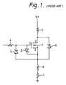
- a semiconductor device having a MOSFET transistor such as the MOSFET 1 with a semiconductor switch such as the thyristor 2 thermally connected to the MOSFET 1 and the two main electrodes of the thyristor 2 connected across the gate G and source S electrodes of the MOSFET is known from Patent Document EP 208970A.
- the thyristor 2 is designed to turn on before a temperature, which may be between 130 and 180°C, critical for the MOSFET 1 is reached. This uses the previously known failure mode of triacs and thyristors, that they will turn on above a certain temperature, in order to provide temperature protection for a MOSFET transistor.
- the thyristor 2 turns on and causes the MOSFET 1 to turn off by reducing the gate-source voltage below its threshold value. This has the advantage of protecting the MOSFET against overload conditions of excessive current or an inadequate thermal environment while allowing it to exploit all specified combinations of power dissipation and ambient temperature.
- the MOSFET 1 is on and a load 3 connected thereto is in normal condition then the thyristor 2 is off, whereas if the MOSFET 1 is on and the load 3 is in short-circuit condition then the heat generated in the MOSFET 1 causes the thyristor 2 to turn on above a predetermined temperature and the turned on condition of the thyristor 2 causes the MOSFET 1 to turn off.
- the short-circuit current through the MOSFET 1 is typically 80 amps.
- the gate-source voltage of the MOSFET 1 falls rapidly to a low value and the drain-source current of the MOSFET is blocked.
- parasitic wiring inductances 7,8 in the power feeds to the MOSFET drain and source electrodes.
- the turn-off speed of the MOSFET 1 responsive to the thyristor 2 turning on will be high and voltage transients generated by the parasitic inductances 7,8 when the drain-source current of the MOSFET is blocked can be high enough to cause catastrophic and permanent damage to the MOSFET 1 if they are not suppressed.
- the drain-source voltage of the MOSFET 1 must be kept to less than 50 volts to avoid damage.
- the zener diode 6 provides the necessary voltage transient suppression by providing an alternative current path for dissipation of the transient energy while limiting the transient drain-source voltage and hence also the transient drain-gate voltage.
- a disadvantage of the known arrangement described above with reference to Figure 1 is that the zener diode 6 needs to be a large and expensive power device because it is required to have a low slope resistance, that is to say that it has to conduct the initial high short-circuit current of typically 80A without this producing a voltage rise from its nominal zener voltage sufficient to over-rate the MOSFET drain-source or drain-gate junctions.
- the amount of transient energy generated by the parasitic wiring inductances 7,8 and hence the time taken for it to dissipate through the zener diode 6 depends on the size of these inductances.
- the large size of the zener diode 6 is itself a problem since this makes it difficult to mount it close to the MOSFET device. If it is not mounted close enough and the zener diode leads are of significant length then their parasitic inductance will delay the current build up in the zener diode possibly sufficient to allow a significant voltage surge on the MOSFET.
- An automotive vehicle electrical system is an example of a system in which power MOSFET transistors may be advantageously temperature protected each by a semiconductor switch as described above, but in which the disadvantageous expense of using a power zener diode in each case to suppress the voltage transients arising from the action of the semiconductor switch can be significant.
- One such system is known from the article "Multiplexing for the automotive industry" by W.R.Betts in GEC REVIEW, Vol.2, No.1, 1986 at pages 32 to 36.
- a central master unit including a microcomputer is connected by low current signalling links in a star wired arrangement to a number of remote, non-intelligent, slave units.
- Manually operable switches, sensors and high current loads are connected to the slave units and their interaction is controlled from the master unit by means of time slot assignment multiplex.
- remote switching of power MOSFETs in the slave units controls the high current loads connected to them.
- Such a system could, for example, have approximately 20 slave units each with 16 time multiplexed channels nearly half of which have a load connected to them.
- each power MOSFET is temperature protected by a semiconductor switch as described above with a power zener diode for voltage transient protection as described above, then the temperature and voltage transient protected MOSFETs can account for approximately half the total electronics cost of the system with the power zener diodes accounting for approximately one tenth of this total electronics cost.
- An object of the invention is to provide an alternative means for suppressing voltage transients associated with the power MOSFET temperature protection action of the semiconductor switch as described above, which alternative avoids the use of an expensive and large power zener diode as described above.
- the voltage transient suppression means inlcudes first suppression means for limiting to a predetermined value the drain-gate voltage due to the initial parasitically induced voltage excursion at the drain electrode when the semiconductor switch turns on, and second suppression means responsive to the initial parasitically induced voltage excursion at the source electrode when the semiconductor switch turns on to establish an initial gate-source voltage sufficient to keep the MOSFET on but not greater than a predetermined value, such that the voltage transient suppression means allows the transient energy to dissipate by current conduction through the MOSFET with the turn-off time of the MOSFET being dependent on the value of said parasitic wiring inductances.
- the first suppression means includes a first zener diode and a rectifying diode conected in series between the drain and gate electrodes
- the second suppression means includes a second zener diode connected across the gate and source electrodes
- the second suppression means also includes the first suppression means together with a series combination of the semiconductor switch and a resistance, one end of said series combination being connected to the gate electrode and the other end of said series combination being connected in use to a reference voltage.
- the MOSFET transistor, the first zener diode, the rectifying diode, the semiconductor switch and the resistance may all be within a power MOSFET device package having the usual three terminals for connection to the drain, gate and source electrodes and a fourth terminal for connection in use to said reference voltage.
- the second zener diode may also be within the power MOSFET device package.
- the just described arrangement is modified in that the other end of said series combination is connected to the source electrode.
- the MOSFET transistor, the first zener diode, the rectifying diode, the semiconductor switch and the resistance may all be within a power MOSFET device package having the usual three terminals for connection to the drain, gate and source electrodes.
- the second zener diode may also be within the power MOSFET device package.
- the resistance part of the series combination may be an inherent series resistance of the semiconductor switch.
- the first zener diode and the series combination of the semiconductor switch and resistance provide two negative feedback mechanisms which combine to control the turn-off speed of the MOSFET.
- the first negative feedback mechanism is responsive to the parasitically induced voltage excursion at the drain electrode and the second negative feedback mechanism is responsive to the parasitically induced voltage excursion at the source electrode.
- the turn-off of the MOSFET will be sufficiently slow but no slower than is necessary to maintain the drain-gate voltage and the drain-source voltage at safe values however high the parasitic inductances may be.
- the MOSFET is maintained on for as long but no longer than is necessary to dissipate the transient energy, so that if the parasitic inductances are low then the time for which the MOSFET remains at a potentially damaging high temperature is reduced accordingly.
- the energy of the voltage transient produced when the semiconductor switch turns on is allowed to dissipate in a controlled manner through the MOSFET itself, and so the prior art power zener diode is not required.
- the first zener diode in the preferred embodiments of the invention does not carry the high short-circuit switching current but only a small signal current which controls the MOSFET, so that this zener diode will be a small inexpensive device.
- the second zener diode in the preferred embodiments is that conventionally used to limit the gate-source voltage of the MOSFET in normal operation and is also a small inexpensive device.
- An added advantage of the preferred embodiments of the invention is that they also protect the MOSFET against externally generated voltage transients which may occur when the MOSFET is off during normal operation.
- the first zener diode will operate to limit the drain-gate voltage by raising the gate voltage to turn the MOSFET on and so dissipate the transient.
- a resistance having a specified value can be inserted in series with the semiconductor switch 2 between the gate and source electrodes or the inherent series resistance of the semiconductor switch 2 can be chosen to have this specified value.
- this resistance will provide an RC time constant which increases the inherent turn-off time of the MOSFET to a particular value and allows voltage transient energy due to the two parasitic wiring inductances to dissipate through the MOSFET during this RC turn-off time.
- the value chosen for the resistance would have to be large enough to provide in conjunction with the lowest expected gate-source capacitance a turn-off time large enough safely to suppress the transient drain and source voltage excursions due to the highest expected parasitic wiring inductances.
- the turn-off time of the MOSFET will thus always have to be longer than is absolutely necessary for suppression of the voltage transient, and so the MOSFET will continue to conduct and be at a potentially damaging high temperature for longer than is necessary after the semiconductor switch turns on.
- this arrangemnt would not protect the MOSFET against externally generated voltage transients when the MOSFET is off during normal operation and a zener diode might need to be provided across the drain and source electrodes to give this protection.
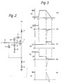
- the power MOSFET switch arrangement shown has a semiconductor device having a power MOSFET transistor 1 with a semiconductor switch in the form of a thyristor 2 thermally connected to the MOSFET 1 and the two main electrodes of the thyristor 2 connected across the gate G and source S electrodes.
- a high current load 3 is connected between the MOSFET source S and a ground connection, and the MOSFET drain D is connected to a positive potential +V volts.
- a control signal is applied to the gate G of the MOSFET via a resistor 4 and is limited by a zener diode 5.
- the control signal turns the power MOSFET 1 on and off to operate the high current load 3. If the MOSFET 1 is on and the load 3 is in normal condition then the thyristor 2 is off, whereas if the MOSFET 1 is on and the load 3 is in short-circuit condition then the heat generated in the MOSFET 1 causes the thyristor 2 to turn on above a predetermined temperature of say 150°C and the turned on condition of the thyristor 2 causes the gate-source voltage to fall whereby the drain-source current is blocked and the MOSFET 1 is turned off and thus protected from damage which would occur if it remained at that predetermined temperature.
- One main electrode of the thyristor 2 is connected to the gate electrode G, optionally via a low value resistance 9 whose function will be explained later.
- the other main electrode of the thyristor 2 is connected via a resistance 10 to a ground connection.
- a zener diode 11 and a rectifying diode 12 are connected in series between the drain D and gate G electrodes.
- the zener diode 11, rectifying diode 12, thyristor 2 and resistance 10, together with the zener diode 5, provide means for suppressing voltage transients generated by the parasitic inductances 7,8 when the MOSFET 1 turns off responsive to the thyristor 2 turning on.
- the zener diode 11 and the rectifying diode 12 form first suppression means for limiting to a predetermined value the drain-gate voltage due to the initial parasitically induced voltage excursion at the drain electrode D when the thyristor 2 turns on.
- the first and second suppression means allows the voltage transient energy generated by the parasitic wiring inductances 7,8 to dissipate the current conduction through the MOSFET with the turn-off time of the MOSFET being dependent on the values of the inductances 7,8.
- the semiconductor switch 2 may be a triac instead of a thyristor.
- the resistance 10 may be an inherent series resistance of the semiconductor switch 2.
- the MOSFET transistor 1 and thyristor 2 together with the optional resistance 9, the zener diode 11, rectifying diode 12, and the resistance 10 may all be within a power MOSFET device package having the usual three terminals for connection to the drain, gate and source electrodes with an additional fourth terminal for connection of the resistance 10 to ground potential.
- the full line waveforms of graphs (a), (b), (c) and (d) respectively show the current Id through the MOSFET 1, and the voltages Vs at its source electrode, Vd at its drain electrode and Vg at its gate electrode from an initial time when the MOSFET is on with the load 3 in normal condition, through time t1 when the load 3 goes to short-circuit condition, through time t2 when the thyristor 2 turns on, to time t3 when the MOSFET turns off.
- the dotted line waveforms on graphs (a), (b), (c) and (d) and the waveform on graph (e) show the operation of the prior art arrangement of Figure 1 for comparison.
- the drain voltage Vd and source voltage Vs will both be approximately at the potential +V
- the gate voltage Vg will be at a high value determined by the zener diode 5
- the rectifying diode 12 will ensure that the zener diode 11 does not conduct in its forward direction
- the thyristor 2 will be turned off and current will not flow through the resistance 10
- the current Id through the MOSFET 1 will be determined by the resistance of the load 3.
- the potential +V may be the battery voltage 12 volts and the load 3 may be a headlamp bulb.
- both Vd and Vs will be approximately at 12 volts with the drain-source voltage Vds approximately 0.5 volts, Vg may be at 20 volts and Id may be 5 amps.
- Vg may be at 20 volts and Id may be 5 amps.
- the load 3 goes to short-circuit condition at time t2 the source voltage Vs drops to ground potential at 0 volts, the gate voltage Vg accordingly drops to 8 volts as determined by the zener diode 5, and the current Id rises to a short-circuit value determined by the transconductance of the MOSFET 1 and the zener voltage of the zener diode 5.
- the short-circuit value of the current Id after time t1 may typically be 80 amps.
- the heat generated by this high short-circuit current through the MOSFET 1 raises its temperature and hence also raises the temperature of the thermally connected thyristor 2 until at time t2 the thyristor 2 goes above a predetermined temperature of, for example, 150°C which causes it to turn on.
- the thyristor 2 turning on at time t2 causes the gate voltage Vg to drop towards 0V.
- the drain-source current Id is not immediately blocked, owing to the parasitic wiring inductances 7,8 which respectively cause an initial positive excursion of the drain voltage Vd and an initial negative excursion of the source voltage Vs, and owing to the action of the means for suppressing these voltage excursions provided in the arrangement of Figure 2.
- the initially induced voltage excursions at the drain and source electrodes at time t2 would be limited by the zener voltage of the zener diode 6 to ensure a safe value of the drain-source voltage Vds, for example 50 volts.
- the actual values of the excursions of Vd and Vs would depend on the relative values of the inductances 7,8 but in practice would be about the same, for example 19 volts each way with Vd going initially to +31 volts and Vs going initially to -19 volts,
- the gate voltage Vg in the arrangement of Figure 1 would follow the source voltage Vs from time t2.
- the MOSFET current Id would fall rapidly to zero at the time t2 and the zener diode 6 would provide an alternative path for the blocked MOSFET current, the zener diode current Iz starting at the short-circuit current value at time t2.
- the current Iz would reduce to zero at a time t4 at which time the MOSFET drain voltage Vd would reach 12 volts, and the source and gate voltages Vs and Vg would reach 0 volts.
- the zener voltage of the zener diode 12 is chosen to be a value which will in practice always be reached due to the positive induced excursion of the drain voltage Vd at time t2, will ensure a safe value for the drain-gate voltage Vdg at that time and will also help to ensure a safe value for the drain-source voltage Vds.
- This zener voltage may be, for example, 20 volts.
- the gate voltage will be held a little above 0 volts partly by the tendency of the drain voltage Vd to go above 42 volts.
- the negative excursion of the source voltage Vs at time t2 will, by means of the resistance 10, establish a gate-source voltage Vgs which will exceed the threshold gate-source voltage so as to keep the MOSFET on and thereby limit that negative excursion of the source votage Vs.
- the gate voltage will be held a little above 0 volts also partly by the resistance 10.
- the gate-source voltage Vgs at time t2 will not exceed the zener voltage of the zener diode 5, for example 8 volts as previously mentioned, so that an absolute safe limit for the drain-source voltage at time t2 is set by the combined zener voltages of zener diodes 11 and 5, for example 38 volts.
- the actual value of the gate-source voltage established at time t2 depends on the current which is passed by the zener diode 11 through the resistance 10 and the value of the resistance 10.
- This signal current, which controls the MOSFET from time t2 may be for example 5mA such that for a resistance 10 of, for example, 1Kohm, a gate-source voltage Vgs of 5 volts is established at time t2.
- the limitation of the positive excursion of the drain voltage Vd and the limitation of the negative excursion of the source voltage Vs at the time t2 may each be considered as by operation of a respective negative feedback mechanism.
- the current Id through the MOSFET 1 is initially maintained at its short-circuit value and then, as the energy of the voltage transients generated by the parasitic inductances 7,8 dissipates by current conduction through the MOSFET, the current Id falls at a rate determined by the particular values of the inductances 7,8 to zero at time t3.
- the source voltage Vs rises quickly from its negative excursion limit, of for example, nearly -5 volts, back to 0 volts at time t3
- the drain voltage Vd drops slowly from its positive excursion limit until nearly time t3 when it then drops to 12 volts
- the gate voltage Vg drops slowly from just above 0 volts to 0 volts at time t3.
- the action of the low resistance 9 is to reduce any tendency to oscillation between times t2 and t3 due to any parasitic capacitance, for example in the zener diode 11 and rectifying diode 12.
- the arrangement of Figure 2 will also protect the MOSFET 1 against externally generated voltage transients which may occur when the MOSFET is off during normal operation.
- the zener diode 11 will operate to limit the drain-gate voltage by raising the gate voltage to turn the MOSFET on and so dissipate the transient.
- a voltage spike applied in the same circumstances to the source electrode would in any case be suppressed by turning the MOSFET on.
- the ground connection of one end of the resistance 10 in the arrangement of Figure 2 may be considered as a reference voltage connection.
- the transient voltage excursions of the drain and source electrodes as shown in Figure 3 may be considered as occuring relative to this reference voltage of 0 volts.
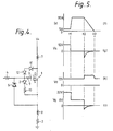
- the arrangement is the same as that shown in Figure 2 with the modification that the end of the resistance 10 away form the gate electrode G is connected to the source electrode S.
- the operation of the arrangement shown in Figure 4 is essentially the same as the Figure 2 arrangement in its suppression of the drain and source voltage excursions when the thyristor 2 turns on, so as to limit the drain-gate and drain-source voltages to safe values while transient energy due to the parasitic inductances 7,8 is dissipated by current conduction through the MOSFET with a turn-off time determined by these inductances.
- the waveforms (f), (g), (h) and (i) show the current Id and the voltages Vs, Vd and Vg for the Figure 4 arrangement through the times t1, t2 to t3 which respectively indicate the load 3 going short-circuit, the thyristor 2 turning on and the MOSFET 1 turning off in the same manner as for Figure 3.
- the waveform (f) for the current Id is the same as the waveform (a) shown in Figure 3.
- the waveforms for the source, drain and gate voltages Vs, Vd and Vg up to the time t2 when the thyristor 2 turns on are the same as shown in Figure 3.
- the arrangement of Figure 4 controls the voltages Vs, Vd and Vg in a similar manner to the arrangement of Figure 2 except that instead of these three voltages being controlled relative to 0 volts as a reference it is rather the case that the drain voltage Vd and the gate voltage Vg are controlled relative to the source voltage Vs as a reference.
- the drain voltage Vd goes positive above 12 volts responsive to the parasitic inductance 7
- the source voltage Vs goes negative below 0 volts responsive to the parasitic inductance 8
- the gate voltage Vg follows the source voltage below 0 volts.
- a possible disadvantage of the arrangement of Figure 4 is that the voltage transient is applied, at a reduced level, to the resistor 4 and its associated circuitry because the gate voltage Vg is allowed to go negative by an undefined amount according to the value of the parasitic inductance 8.
- the significant advantage of the Figure 4 arrangement is that the MOSFET transistor 1 and thyristor 2 together with the optional resistance 9, the zener diode 11, rectifying diode 12, and the resistance 10 may all be within a standard power MOSFET device package having only the usual three terminals for connection to the drain, gate and source electrodes.
- FIG. 2 and Figure 4 show a load 3 connected to the source electrode of the MOSFET transistor 1. These arrangements would work equally well if the load were instead connected to the drain electrode of the MOSFET. In this case, for both arrangements, Vs and Vd would both be at approximately 0 volts and Vg would be at 8 volts before time t1. When the load connected to the drain electrode goes short-circuit at time t1 Vd rises to 12 volts, and Vg and Vs remain respectively at 8 volts and 0 volts. From time t2 when the thyristor 2 turns on to time t3 when the MOSFET turns off, the voltages Vs, Vd and Vg would behave exactly as has been shown in Figures 3 and 5.
Landscapes
- Electronic Switches (AREA)
Applications Claiming Priority (2)
| Application Number | Priority Date | Filing Date | Title |
|---|---|---|---|
| GB8810750 | 1988-05-06 | ||
| GB888810750A GB8810750D0 (en) | 1988-05-06 | 1988-05-06 | Mosfet power switch arrangements |
Publications (1)
| Publication Number | Publication Date |
|---|---|
| EP0340918A2 true EP0340918A2 (de) | 1989-11-08 |
Family
ID=10636461
Family Applications (1)
| Application Number | Title | Priority Date | Filing Date |
|---|---|---|---|
| EP89303445A Withdrawn EP0340918A2 (de) | 1988-05-06 | 1989-04-07 | Leistungs-MOSFET-Schalteranordnungen |
Country Status (6)
| Country | Link |
|---|---|
| EP (1) | EP0340918A2 (de) |
| JP (1) | JPH01318430A (de) |
| KR (1) | KR890017877A (de) |
| CN (1) | CN1037810A (de) |
| AU (1) | AU3382289A (de) |
| GB (2) | GB8810750D0 (de) |
Cited By (7)
| Publication number | Priority date | Publication date | Assignee | Title |
|---|---|---|---|---|
| DE4131949A1 (de) * | 1990-09-25 | 1992-04-30 | Mitsubishi Electric Corp | Schalteinrichtung fuer lasergeraete |
| EP0553443A3 (en) * | 1992-01-31 | 1994-09-14 | Hella Kg Hueck & Co | Circuit for operating and monitoring inductive loads, especially for magnetic valves, in an antilock regulating-system |
| EP0645889A1 (de) * | 1993-09-13 | 1995-03-29 | Siemens Aktiengesellschaft | Verfahren und Vorrichtung zur Begrenzung der Stromfallgeschwindigkeit beim Ausschalten von Leistungshalbleiterschaltern mit MOS-Steuereingang |
| DE19741214C1 (de) * | 1997-09-18 | 1998-12-17 | Siemens Ag | Temperaturgeschützter Halbleiterschalter |
| WO1999030418A1 (de) * | 1997-12-09 | 1999-06-17 | Mannesmann Vdo Ag | Schaltungsanordnung zum getakteten ansteuern einer last |
| EP0949736A1 (de) * | 1998-04-10 | 1999-10-13 | STMicroelectronics S.r.l. | Elektronische Brücken- und Halbbrückenschaltungen mit Unterdrückung von Spitzenspannungen auf der Versorgungsleitung |
| US7768290B2 (en) | 2007-03-22 | 2010-08-03 | Huawei Technologies Co., Ltd. | Circuit and apparatus for detecting electric current |
Families Citing this family (6)
| Publication number | Priority date | Publication date | Assignee | Title |
|---|---|---|---|---|
| JPH03117017A (ja) * | 1989-09-28 | 1991-05-17 | Nec Corp | トランジスタ出力回路 |
| JPH0722928A (ja) * | 1993-06-24 | 1995-01-24 | Nec Corp | 半導体集積回路装置 |
| CN100407572C (zh) * | 2004-08-02 | 2008-07-30 | 阎跃军 | 场效应管偏置电路 |
| JP5907102B2 (ja) * | 2013-03-22 | 2016-04-20 | トヨタ自動車株式会社 | 半導体装置 |
| JP6052068B2 (ja) * | 2013-06-07 | 2016-12-27 | 株式会社デンソー | 半導体装置の保護回路 |
| CN113381599B (zh) * | 2021-06-29 | 2022-11-29 | 哈尔滨工业大学 | 一种并联SiC MOSFET安全工作域计算方法 |
-
1988
- 1988-05-06 GB GB888810750A patent/GB8810750D0/en active Pending
-
1989
- 1989-04-05 GB GB8907644A patent/GB2218289A/en not_active Withdrawn
- 1989-04-07 EP EP89303445A patent/EP0340918A2/de not_active Withdrawn
- 1989-04-25 JP JP1103619A patent/JPH01318430A/ja active Pending
- 1989-04-27 AU AU33822/89A patent/AU3382289A/en not_active Abandoned
- 1989-05-04 KR KR1019890006027A patent/KR890017877A/ko not_active Withdrawn
- 1989-05-06 CN CN89103081A patent/CN1037810A/zh active Pending
Cited By (11)
| Publication number | Priority date | Publication date | Assignee | Title |
|---|---|---|---|---|
| DE4131949A1 (de) * | 1990-09-25 | 1992-04-30 | Mitsubishi Electric Corp | Schalteinrichtung fuer lasergeraete |
| US5305338A (en) * | 1990-09-25 | 1994-04-19 | Mitsubishi Denki Kabushiki Kaisha | Switch device for laser |
| DE4131949C2 (de) * | 1990-09-25 | 1996-10-10 | Mitsubishi Electric Corp | Schalteinrichtungen für ein entladungserregtes Impulslasergerät |
| EP0553443A3 (en) * | 1992-01-31 | 1994-09-14 | Hella Kg Hueck & Co | Circuit for operating and monitoring inductive loads, especially for magnetic valves, in an antilock regulating-system |
| US5515278A (en) * | 1992-01-31 | 1996-05-07 | Hella Kg Hueck & Co. | Circuit for controlling, monitoring, and terminating control of, inductive loads, particularly magnetic valves in an anti-lock control system |
| EP0645889A1 (de) * | 1993-09-13 | 1995-03-29 | Siemens Aktiengesellschaft | Verfahren und Vorrichtung zur Begrenzung der Stromfallgeschwindigkeit beim Ausschalten von Leistungshalbleiterschaltern mit MOS-Steuereingang |
| DE19741214C1 (de) * | 1997-09-18 | 1998-12-17 | Siemens Ag | Temperaturgeschützter Halbleiterschalter |
| WO1999030418A1 (de) * | 1997-12-09 | 1999-06-17 | Mannesmann Vdo Ag | Schaltungsanordnung zum getakteten ansteuern einer last |
| EP0949736A1 (de) * | 1998-04-10 | 1999-10-13 | STMicroelectronics S.r.l. | Elektronische Brücken- und Halbbrückenschaltungen mit Unterdrückung von Spitzenspannungen auf der Versorgungsleitung |
| US6160694A (en) * | 1998-04-10 | 2000-12-12 | Stmicroelectronics S.R.L. | Electronic bridge and half-bridge circuits with suppression of high-voltage transients on the power supply line |
| US7768290B2 (en) | 2007-03-22 | 2010-08-03 | Huawei Technologies Co., Ltd. | Circuit and apparatus for detecting electric current |
Also Published As
| Publication number | Publication date |
|---|---|
| AU3382289A (en) | 1989-11-09 |
| JPH01318430A (ja) | 1989-12-22 |
| GB8810750D0 (en) | 1988-06-08 |
| GB2218289A (en) | 1989-11-08 |
| CN1037810A (zh) | 1989-12-06 |
| GB8907644D0 (en) | 1989-05-17 |
| KR890017877A (ko) | 1989-12-18 |
Similar Documents
| Publication | Publication Date | Title |
|---|---|---|
| KR102838077B1 (ko) | 보호 버스에서 접지로 연결된 fet 디바이스를 갖는 보호 회로 | |
| US5444591A (en) | IGBT fault current limiting circuit | |
| US5585991A (en) | Protective circuit for protecting load against excessive input voltage | |
| US4420700A (en) | Semiconductor current regulator and switch | |
| EP0340918A2 (de) | Leistungs-MOSFET-Schalteranordnungen | |
| EP0115002B1 (de) | Überspannungs-Schutzschaltung | |
| US10734882B2 (en) | Conversion circuit | |
| US5463521A (en) | Power supply protection circuit | |
| US6687106B1 (en) | Power module | |
| JP5541349B2 (ja) | 半導体装置 | |
| JP5630484B2 (ja) | 半導体装置 | |
| EP0593588B1 (de) | Schutzeinrichtung für schaltung | |
| Chokhawala et al. | IGBT fault current limiting circuit | |
| CN113613937A (zh) | 开关装置、电压供应系统、开关装置操作方法和制造方法 | |
| US20230412167A1 (en) | Power Electronic Module Comprising a Gate-Source Control Unit | |
| KR102733100B1 (ko) | 전력 스위치용 단락보호회로 | |
| JP3918778B2 (ja) | 保護回路 | |
| US12413224B2 (en) | Avalanche protection circuit | |
| CN120880418A (zh) | 栅极感应电压抑制电路及驱动系统 | |
| KR101913964B1 (ko) | Igbt 게이트 구동장치 | |
| Biswas et al. | Safe operation of IGBTs in switching converters |
Legal Events
| Date | Code | Title | Description |
|---|---|---|---|
| PUAI | Public reference made under article 153(3) epc to a published international application that has entered the european phase |
Free format text: ORIGINAL CODE: 0009012 |
|
| AK | Designated contracting states |
Kind code of ref document: A2 Designated state(s): BE DE ES FR GB IT SE |
|
| STAA | Information on the status of an ep patent application or granted ep patent |
Free format text: STATUS: THE APPLICATION HAS BEEN WITHDRAWN |
|
| 18W | Application withdrawn |
Withdrawal date: 19900528 |
|
| R18W | Application withdrawn (corrected) |
Effective date: 19900528 |