EP0340100A1 - Herstellungsverfahren von Speicherkarten und Karten, die nach diesem Verfahren hergestellt sind - Google Patents
Herstellungsverfahren von Speicherkarten und Karten, die nach diesem Verfahren hergestellt sind Download PDFInfo
- Publication number
- EP0340100A1 EP0340100A1 EP89401173A EP89401173A EP0340100A1 EP 0340100 A1 EP0340100 A1 EP 0340100A1 EP 89401173 A EP89401173 A EP 89401173A EP 89401173 A EP89401173 A EP 89401173A EP 0340100 A1 EP0340100 A1 EP 0340100A1
- Authority
- EP
- European Patent Office
- Prior art keywords
- mold
- card
- face
- support element
- support
- Prior art date
- Legal status (The legal status is an assumption and is not a legal conclusion. Google has not performed a legal analysis and makes no representation as to the accuracy of the status listed.)
- Granted
Links
Images
Classifications
-
- G—PHYSICS
- G06—COMPUTING OR CALCULATING; COUNTING
- G06K—GRAPHICAL DATA READING; PRESENTATION OF DATA; RECORD CARRIERS; HANDLING RECORD CARRIERS
- G06K19/00—Record carriers for use with machines and with at least a part designed to carry digital markings
- G06K19/06—Record carriers for use with machines and with at least a part designed to carry digital markings characterised by the kind of the digital marking, e.g. shape, nature, code
- G06K19/067—Record carriers with conductive marks, printed circuits or semiconductor circuit elements, e.g. credit or identity cards also with resonating or responding marks without active components
- G06K19/07—Record carriers with conductive marks, printed circuits or semiconductor circuit elements, e.g. credit or identity cards also with resonating or responding marks without active components with integrated circuit chips
- G06K19/077—Constructional details, e.g. mounting of circuits in the carrier
- G06K19/0772—Physical layout of the record carrier
- G06K19/07724—Physical layout of the record carrier the record carrier being at least partially made by a molding process
-
- B—PERFORMING OPERATIONS; TRANSPORTING
- B29—WORKING OF PLASTICS; WORKING OF SUBSTANCES IN A PLASTIC STATE IN GENERAL
- B29C—SHAPING OR JOINING OF PLASTICS; SHAPING OF MATERIAL IN A PLASTIC STATE, NOT OTHERWISE PROVIDED FOR; AFTER-TREATMENT OF THE SHAPED PRODUCTS, e.g. REPAIRING
- B29C45/00—Injection moulding, i.e. forcing the required volume of moulding material through a nozzle into a closed mould; Apparatus therefor
- B29C45/14—Injection moulding, i.e. forcing the required volume of moulding material through a nozzle into a closed mould; Apparatus therefor incorporating preformed parts or layers, e.g. injection moulding around inserts or for coating articles
- B29C45/14639—Injection moulding, i.e. forcing the required volume of moulding material through a nozzle into a closed mould; Apparatus therefor incorporating preformed parts or layers, e.g. injection moulding around inserts or for coating articles for obtaining an insulating effect, e.g. for electrical components
- B29C45/14647—Making flat card-like articles with an incorporated IC or chip module, e.g. IC or chip cards
-
- B—PERFORMING OPERATIONS; TRANSPORTING
- B29—WORKING OF PLASTICS; WORKING OF SUBSTANCES IN A PLASTIC STATE IN GENERAL
- B29C—SHAPING OR JOINING OF PLASTICS; SHAPING OF MATERIAL IN A PLASTIC STATE, NOT OTHERWISE PROVIDED FOR; AFTER-TREATMENT OF THE SHAPED PRODUCTS, e.g. REPAIRING
- B29C45/00—Injection moulding, i.e. forcing the required volume of moulding material through a nozzle into a closed mould; Apparatus therefor
- B29C45/14—Injection moulding, i.e. forcing the required volume of moulding material through a nozzle into a closed mould; Apparatus therefor incorporating preformed parts or layers, e.g. injection moulding around inserts or for coating articles
- B29C45/14688—Coating articles provided with a decoration
-
- B—PERFORMING OPERATIONS; TRANSPORTING
- B29—WORKING OF PLASTICS; WORKING OF SUBSTANCES IN A PLASTIC STATE IN GENERAL
- B29C—SHAPING OR JOINING OF PLASTICS; SHAPING OF MATERIAL IN A PLASTIC STATE, NOT OTHERWISE PROVIDED FOR; AFTER-TREATMENT OF THE SHAPED PRODUCTS, e.g. REPAIRING
- B29C45/00—Injection moulding, i.e. forcing the required volume of moulding material through a nozzle into a closed mould; Apparatus therefor
- B29C45/14—Injection moulding, i.e. forcing the required volume of moulding material through a nozzle into a closed mould; Apparatus therefor incorporating preformed parts or layers, e.g. injection moulding around inserts or for coating articles
- B29C45/14827—Injection moulding, i.e. forcing the required volume of moulding material through a nozzle into a closed mould; Apparatus therefor incorporating preformed parts or layers, e.g. injection moulding around inserts or for coating articles using a transfer foil detachable from the insert
-
- G—PHYSICS
- G06—COMPUTING OR CALCULATING; COUNTING
- G06K—GRAPHICAL DATA READING; PRESENTATION OF DATA; RECORD CARRIERS; HANDLING RECORD CARRIERS
- G06K19/00—Record carriers for use with machines and with at least a part designed to carry digital markings
- G06K19/06—Record carriers for use with machines and with at least a part designed to carry digital markings characterised by the kind of the digital marking, e.g. shape, nature, code
- G06K19/067—Record carriers with conductive marks, printed circuits or semiconductor circuit elements, e.g. credit or identity cards also with resonating or responding marks without active components
- G06K19/07—Record carriers with conductive marks, printed circuits or semiconductor circuit elements, e.g. credit or identity cards also with resonating or responding marks without active components with integrated circuit chips
- G06K19/077—Constructional details, e.g. mounting of circuits in the carrier
- G06K19/07745—Mounting details of integrated circuit chips
-
- H—ELECTRICITY
- H10—SEMICONDUCTOR DEVICES; ELECTRIC SOLID-STATE DEVICES NOT OTHERWISE PROVIDED FOR
- H10W—GENERIC PACKAGES, INTERCONNECTIONS, CONNECTORS OR OTHER CONSTRUCTIONAL DETAILS OF DEVICES COVERED BY CLASS H10
- H10W90/00—Package configurations
- H10W90/701—Package configurations characterised by the relative positions of pads or connectors relative to package parts
- H10W90/751—Package configurations characterised by the relative positions of pads or connectors relative to package parts of bond wires
- H10W90/754—Package configurations characterised by the relative positions of pads or connectors relative to package parts of bond wires between a chip and a stacked insulating package substrate, interposer or RDL
Definitions
- the present invention relates to a method for producing memory cards, in particular electronic cards, and to cards obtained by implementing said method.
- Memory cards essentially comprise a card body which is generally made of a plastic material and a memory module.
- the memory module is an electronic module essentially comprising a semiconductor chip or "chip” in which an integrated circuit is produced and a printed circuit element on which the chip or the like is fixed and which defines external electrical contact areas.
- the electronic module is fixed in the body of the card in such a way that the electrical contact pads are flush with one of the main faces of the card body.
- the card body has the shape of a rectangular parallelepiped whose thickness must be less than 1 mm and which is defined by standard ISO 7810.
- the edges of the card body serve as a reference for positioning the card in the reader of cards in such a way that the contact areas of the card come into electrical contact with the connector of the card reader.
- the card body must also meet other specifications concerning the quality of the surface condition and the very precise flexural properties both in the longitudinal direction of the card body and in its transverse direction. and in torsion. These specifications are defined by the ISO standard (mentioned above). In addition, the card body must not favor the storage of electrostatic charges.
- an object of the invention is to provide a method for producing a card, in particular a memory card, in which the step of producing the graphics on the card body cannot in itself lead to rejection. from the menu.
- An object of the invention is to provide an embodiment of a memory card, in particular electronic, by overmolding of the card body on the memory module, which also allows, if desired, to produce the graphic elements in particularly attractive economic conditions.
- the method of producing a memory card comprising a card body having two main faces parallel to each other and a memory module having an access face disposed in the first of said main faces of the body card which is characterized in that it comprises the following stages:
- a mold is provided, the imprint of which defines the external shape of said card, We provide a support element, We provide a memory module having an access face, We fix said memory module, by its access face, on one face of the support element, Said support element is placed in said mold so that its periphery is integral with said mold, Plastic material is injected into said mold so that it fills said mold cavity and said module is surrounded by said material, The part thus obtained is removed from the mold and the support element is separated from said part, whereby said module is inserted into said body, and After demolding, a memory card is obtained having a card body having its final shape and in which the electronic module is already installed.
- the support element has, on the face on which the memory module is fixed, printing elements, and during the injection of the plastic material into the mold, said printing elements adhere to the face of the volume of material injected in contact with the support element, whereby a memory card is obtained comprising moreover graphic elements on the first main face of the card body.
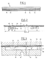
- the support element, bearing the reference 10 comprises a support 12 made of plastic material.
- the support 12 is preferably made of polyester and has a thickness of the order of 25 micrometers.
- On this support 12 which plays the role of mechanical support are produced the printing elements subsequently used to obtain the desired graphics.
- a support element 10 which comprises a plurality of identical patterns, each pattern corresponding to all of the graphics which must be produced on one of the faces of the card body.
- the patterns A and B are shown. Each pattern is separated from the neighboring patterns by a blank space whose utility will be explained later.
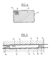
- FIG. 4 shows a card body 30 produced according to the invention.
- the electronic module 32 has been shown, of which only the external electrical contact pads 34 are visible.
- Also shown at 36 are the areas of the card body which include a graphic. The zone 36 leaves open the portion of the face of the card body 30 occupied by the external pads 34 of electrical contact.
- the electronic module 32 comprises a lead frame or a printed circuit element on which the external pads 34 are made, a semiconductor patch 40 fixed on the printed circuit or the lead frame, conductive wires 42 which connect the terminals of the patch 40 to the contact pads 34 and a coating material 44 which surrounds the patch 40 and the wires 42.
- a module 32 is glued to the support 12 at each location 38, so that each pattern has a module.
- the external face of the external contact pads is directly bonded to the support 12.
- a strip is thus obtained formed by the support 12 which comprises on one of its faces a plurality of patterns (A, B ..) each pattern further comprising an electronic module 32.
- the body of the card is produced by injection molding of a plastic material which is preferably ABS.
- Figure 3 shows the mold used. It comprises a fixed part 50 and a movable part 52. These two parts define an imprint 53 which gives the external shape of the card body.
- the fixed part 50 defines by its internal wall 54 one of the main faces of the card body.
- the movable part 52 defines by its internal wall 56 the second main face of the card body and by its internal wall 58 the edge of the card body.
- the fixed 50 and mobile 52 bearing surfaces each have a bearing surface 60 and 62, these two bearing surfaces being normally in mutual contact when the mold is closed.
- the strip formed by the support 12 is placed between the fixed part 50 and the movable part 52 of the mold.
- the strip is positioned relative to the imprint 53 so that the graphics 16 carried by the support 12, and, consequently, the electronic module 32 are perfectly positioned relative to the side wall 58 of the imprint, that is to say with respect to the edge of the card body which will be produced.
- the mold is closed.
- support 12 is pinched between staves 58 and 60 of the two parts of the mold in the zone D of the support 12 which surrounds a pattern.
- the plastic material is injected into the impression 53 by the injection nozzle 64, the ABS is preferably injected at a temperature between 220 ° C. and 280 ° C.
- the nozzle 64 is disposed in the center of the wall 56 of the movable part 52.
- the plastic material fills the imprint 53 by pressing the support 12 against the internal wall 54 of the mold.
- the plastic material surrounds the electronic module 32, with the exception of its face glued to the support 12 and it is in contact with the graphics 16.
- the decorative elements 16 are fixed on the corresponding face of the volume of plastic material by tending to separate from the support 12. This result is obtained by activating the adhesive layer 20 and the release layer 14.
- the injection nozzle opens out 64 in the face 56 of the mold, facing the electronic module. It is also possible to provide several injection nozzles. It is also possible to have injection nozzles in the lateral face 58 of the mold cavity. Preferably then the nozzles are arranged at certain "corners" of the mold imprint.
- the card body is removed from the mold in which the electronic module 32 is inserted and which includes the desired graphics 36 on its main face.
- the support 12 plays a dual role, it allows the realization of graphics, and it ensures the precise positioning of the electronic module with respect to the imprint of the mold and therefore with respect to the card body. Moreover, the outer areas of the module being glued to the support 12, they are protected against possible rising of the injection material which could tend to cover them.
- the support 12 which no longer carries either an electronic module or the graphics remains in the mold after the card has been removed.
- FIG. 5 shows a variant of a mold which can be used to produce an electronic memory card having graphic elements on its two main faces.
- the mold is made up of three parts.
- a first part 70 which is mobile, comprises the part 72 of the mold cavity which defines the first main face of the card body.
- a second movable part 74 comprises the part 76 of the mold cavity which defines the second main face of the card body.
- a third part 78 fixed, which is clamped between the parts 70 and 74 of the mold when the latter is closed, comprises the part 80 of the imprint which defines the edge or the edge of the card body.
- the part 78 of the mold comprises, for example, two injection nozzles 82 and 84.
- the manufacture of a card using the mold of Figure 5 is carried out as follows: the mold is open, that is to say that the parts 70 and 74 are spaced from the fixed part 78. A film 12 supporting printing elements provided with its electronic module 32 is placed between the parts 70 and 78 of the mold as has already been described in connection with FIG. 3.
- a second film 12 ′ supporting printing elements, but without an electronic module, is placed in the same way between the parts 78 and 74 of the mold. Then we close the mold using locking means not shown in Figure 4. Thus the support films 12 and 12 'are integral with the mold since they are pinched between the three parts 70, 74 and 78 of the mold. The plastic material is then injected into the mold by the nozzles 82 and 84, and the card thus obtained is removed from the mold.
- the support film has the sole function of ensuring the positioning and the maintenance of the module in the mold. It is therefore devoid of printing elements.
- the support film must be made of a material which does not adhere to the injection material at its injection temperature c, that is to say at a temperature of the order of 200 to 280 ° C.
- the adhesive material which is used to fix the electronic module to the support film it must have certain characteristics. It must retain its adhesive properties during the filling phase of the mold. Preferably it loses, by thermal effect, its adhesive properties during the cooling phase of the molding material. Thus during the release of the card it is easily separated from the support film.
- the external contact pads are chemically cleaned to remove residual traces of adhesive material.
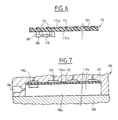
- FIG. 6 shows a support element 170.
- the support element 170 constitutes at the same time the insulating support of the electronic module.
- Element 170 consists of a sheet rectangular 174, for example ABS, which has the shape of the main faces of the card to be produced. In the suitable zone, the sheet 174 has on its external face 174 has metallizations 176 which form the external electrical contact areas of the card.
- a semiconductor patch 178 is fixed on the internal face 174b of the support 174 and connections 180 provide the electrical connection between the terminals of the semiconductor patch 178 and the external pads 176.
- the patch 178 and the connections 180 are preferably coated with insulating material 182.
- graphic prints 183 can be produced on the external face 174 a of the sheet 174 in its part not occupied by the metallizations 176.
- FIG. 7 shows in vertical section a mold 190 which can be used for the production of a card according to the second embodiment of the invention.
- the mold 190 comprises a first part 192 which defines a cavity 194 having the external shape of the body of the card to be produced.
- the part 192 of the mold comprises a plurality of vacuum systems 200 opening into the main face 192 a of the cavity 194. It also comprises an injection channel 196 opening into a "corner" of the cavity 194.
- the second part 198 of the mold 190 defines the second main face 198 a of the card body.
- the manufacture of a memory card according to this second embodiment is obtained in the following manner:
- the support element 170 which also includes the electronic module 182 is placed against the face 192 a of the part 192 of the mold.
- the vacuum systems are made active, which keeps the element 170 closed against the face 192a.
- We then close the mold by fixing the part 198 on the part 192.
- Through the injection channel 196 a suitable plastic material is penetrated which fills the cavity 194 and adheres to the internal face of the support elements 170.
- the injection material is the same as that which constitutes the support element 170.
- a memory card is thus produced which optionally includes on one of its main faces the graphic elements, graphic elements which were produced on the support element before the actual production of the card.
Landscapes
- Engineering & Computer Science (AREA)
- Manufacturing & Machinery (AREA)
- Mechanical Engineering (AREA)
- Computer Hardware Design (AREA)
- Microelectronics & Electronic Packaging (AREA)
- Physics & Mathematics (AREA)
- General Physics & Mathematics (AREA)
- Theoretical Computer Science (AREA)
- Credit Cards Or The Like (AREA)
- Injection Moulding Of Plastics Or The Like (AREA)
- Instructional Devices (AREA)
Applications Claiming Priority (4)
| Application Number | Priority Date | Filing Date | Title |
|---|---|---|---|
| FR8805671 | 1988-04-28 | ||
| FR8805671A FR2630843B1 (fr) | 1988-04-28 | 1988-04-28 | Procede de realisation de cartes comportant des elements graphiques et cartes obtenues par ledit procede |
| FR8812088 | 1988-09-16 | ||
| FR8812088A FR2636755B1 (fr) | 1988-09-16 | 1988-09-16 | Procede de realisation de cartes a memoire et cartes obtenues par ledit procede |
Publications (2)
| Publication Number | Publication Date |
|---|---|
| EP0340100A1 true EP0340100A1 (de) | 1989-11-02 |
| EP0340100B1 EP0340100B1 (de) | 1993-12-29 |
Family
ID=26226631
Family Applications (2)
| Application Number | Title | Priority Date | Filing Date |
|---|---|---|---|
| EP89401173A Revoked EP0340100B1 (de) | 1988-04-28 | 1989-04-25 | Herstellungsverfahren von Speicherkarten und Karten, die nach diesem Verfahren hergestellt sind |
| EP89401172A Ceased EP0340099A1 (de) | 1988-04-28 | 1989-04-25 | Herstellungsverfahren von Speicherkarten mit graphischen Elementen und Karten, die nach diesem Verfahren hergestellt sind |
Family Applications After (1)
| Application Number | Title | Priority Date | Filing Date |
|---|---|---|---|
| EP89401172A Ceased EP0340099A1 (de) | 1988-04-28 | 1989-04-25 | Herstellungsverfahren von Speicherkarten mit graphischen Elementen und Karten, die nach diesem Verfahren hergestellt sind |
Country Status (5)
| Country | Link |
|---|---|
| US (2) | US4961893A (de) |
| EP (2) | EP0340100B1 (de) |
| JP (2) | JP2812485B2 (de) |
| DE (1) | DE68911738T2 (de) |
| ES (1) | ES2049831T3 (de) |
Cited By (27)
| Publication number | Priority date | Publication date | Assignee | Title |
|---|---|---|---|---|
| EP0412893A1 (de) * | 1989-08-07 | 1991-02-13 | Schlumberger Industries | Verfahren zum Herstellen von Kartenkörpern und Karten mit graphischen Elementen und so erhaltene Karten |
| FR2659157A2 (fr) * | 1989-05-26 | 1991-09-06 | Lemaire Gerard | Procede de fabrication d'une carte dite carte a puce, et carte obtenue par ce procede. |
| FR2661761A1 (fr) * | 1990-05-07 | 1991-11-08 | Mitsubishi Electric Corp | Carte a circuit integre. |
| FR2673017A1 (fr) * | 1991-02-18 | 1992-08-21 | Schlumberger Ind Sa | Procede de fabrication d'un module electronique pour carte a memoire et module electronique ainsi obtenu. |
| EP0488485A3 (en) * | 1990-11-27 | 1992-11-19 | Mannesmann Aktiengesellschaft | Method and apparatus for manufacturing a decorated chip-card |
| FR2687817A1 (fr) * | 1991-12-26 | 1993-08-27 | Mitsubishi Electric Corp | Carte a circuit integre mince et procede de fabrication. |
| FR2704961A1 (fr) * | 1993-05-04 | 1994-11-10 | Schlumberger Ind Sa | Procédé de fabrication de cartes à mémoire. |
| US5367766A (en) * | 1990-08-01 | 1994-11-29 | Staktek Corporation | Ultra high density integrated circuit packages method |
| US5377077A (en) * | 1990-08-01 | 1994-12-27 | Staktek Corporation | Ultra high density integrated circuit packages method and apparatus |
| EP0649719A1 (de) * | 1993-10-26 | 1995-04-26 | Siemens Aktiengesellschaft | Verfahren zur Herstellung von Chipkarten mittels Spritzgiessen |
| US5420751A (en) * | 1990-08-01 | 1995-05-30 | Staktek Corporation | Ultra high density modular integrated circuit package |
| US5446620A (en) * | 1990-08-01 | 1995-08-29 | Staktek Corporation | Ultra high density integrated circuit packages |
| US5475920A (en) * | 1990-08-01 | 1995-12-19 | Burns; Carmen D. | Method of assembling ultra high density integrated circuit packages |
| GB2295118A (en) * | 1994-10-07 | 1996-05-22 | Three View Technology Co Ltd | PCMCIA Card manufacturing process |
| WO1997023843A1 (de) * | 1995-12-22 | 1997-07-03 | Sempac Sa | Verfahren zur herstellung einer chipkarte für kontaktlosen betrieb |
| US5702985A (en) * | 1992-06-26 | 1997-12-30 | Staktek Corporation | Hermetically sealed ceramic integrated circuit heat dissipating package fabrication method |
| WO1997050056A1 (de) * | 1996-06-24 | 1997-12-31 | Siemens Aktiengesellschaft | Systemträger für die montage einer integrierten schaltung in einem spritzgussgehäuse |
| WO1998042488A1 (fr) * | 1997-03-21 | 1998-10-01 | Tlog | Procede d'inclusion d'etiquette electronique dans la paroi d'un objet thermotransforme, dispositif preparatoire pour ce procede, et objet moule obtenu par ce procede |
| US6025642A (en) * | 1995-08-17 | 2000-02-15 | Staktek Corporation | Ultra high density integrated circuit packages |
| US6031242A (en) * | 1998-01-23 | 2000-02-29 | Zevatech, Inc. | Semiconductor die in-flight registration and orientation method and apparatus |
| US6077022A (en) * | 1997-02-18 | 2000-06-20 | Zevatech Trading Ag | Placement machine and a method to control a placement machine |
| US6135339A (en) * | 1998-01-26 | 2000-10-24 | Esec Sa | Ultrasonic transducer with a flange for mounting on an ultrasonic welding device, in particular on a wire bonder |
| US6157870A (en) * | 1997-02-18 | 2000-12-05 | Zevatech Trading Ag | Apparatus supplying components to a placement machine with splice sensor |
| US6185815B1 (en) | 1997-12-07 | 2001-02-13 | Esec Sa | Semiconductor mounting apparatus with a chip gripper travelling back and forth |
| CN1113314C (zh) * | 1997-07-10 | 2003-07-02 | 沙诺夫公司 | 用于远程地识别一个电子编码物品的方法与装置 |
| EP1780662A1 (de) * | 2005-10-27 | 2007-05-02 | Axalto SA | Verstärktes Chipkartenmodul und Herstellungsverfahren dafür |
| US8087591B2 (en) | 2004-06-09 | 2012-01-03 | Giesecke & Devrient Gmbh | Method for producing a portable data carrier |
Families Citing this family (62)
| Publication number | Priority date | Publication date | Assignee | Title |
|---|---|---|---|---|
| US5387306A (en) * | 1988-06-21 | 1995-02-07 | Gec Avery Limited | Manufacturing integrated circuit cards |
| JPH0767874B2 (ja) * | 1989-03-31 | 1995-07-26 | リズム時計工業株式会社 | Icカードの製造方法 |
| US5244840A (en) * | 1989-05-23 | 1993-09-14 | Mitsubishi Denki Kabushiki Kaisha | Method for manufacturing an encapsulated IC card having a molded frame and a circuit board |
| US5417905A (en) * | 1989-05-26 | 1995-05-23 | Esec (Far East) Limited | Method of making a card having decorations on both faces |
| DE3926578C1 (de) * | 1989-08-11 | 1990-07-26 | Leonhard Kurz Gmbh & Co, 8510 Fuerth, De | |
| DE3929299A1 (de) * | 1989-08-11 | 1991-02-14 | Kurz Leonhard Fa | Verfahren zur herstellung von karten |
| JP2560895B2 (ja) * | 1990-07-25 | 1996-12-04 | 三菱電機株式会社 | Icカードの製造方法およびicカード |
| FR2668096B1 (fr) * | 1990-10-19 | 1993-01-22 | Schlumberger Ind Sa | Procede de fabrication de carte a memoire apte a recevoir une image photographique et carte ainsi obtenue. |
| US5681356A (en) * | 1991-05-10 | 1997-10-28 | Gao Gesellschaft Fur Automation Und Organisation Mbh | Method and apparatus for producing a plastic molded chip card having reduced wall thickness |
| JP2774906B2 (ja) * | 1992-09-17 | 1998-07-09 | 三菱電機株式会社 | 薄形半導体装置及びその製造方法 |
| FR2702067B1 (fr) * | 1993-02-23 | 1995-04-14 | Schlumberger Ind Sa | Procédé et dispositif de fabrication de cartes à mémoire. |
| WO1995019251A1 (en) * | 1994-01-13 | 1995-07-20 | Citizen Watch Co., Ltd. | Method of resin-sealing semiconductor devices |
| US5626339A (en) * | 1994-02-03 | 1997-05-06 | Huffy Corporation | Structural foam basketball backboard with inmold graphics |
| US5916047A (en) * | 1994-02-03 | 1999-06-29 | Huffy Corporation | Portable basketball goal support system with separate ballast tank |
| US5980400A (en) * | 1994-02-03 | 1999-11-09 | Huffy Corporation | Compression molded basketball components with inmold graphics |
| JP3442877B2 (ja) * | 1994-02-21 | 2003-09-02 | 富士通株式会社 | 樹脂成形品及びその製造方法 |
| DE4435802A1 (de) * | 1994-10-06 | 1996-04-11 | Giesecke & Devrient Gmbh | Verfahren zur Herstellung von Datenträgern mit eingebetteten Elementen und Vorrichtung zur Durchführung des Verfahrens |
| US5846477A (en) * | 1994-12-08 | 1998-12-08 | Nitto Denko Corporation | Production method for encapsulating a semiconductor device |
| DE29502080U1 (de) * | 1995-02-09 | 1995-03-23 | Interlock Ag, Schlieren | Vorrichtung zur Herstellung von Ausweiskarten und danach hergestellte Ausweiskarte |
| US5819394A (en) * | 1995-02-22 | 1998-10-13 | Transition Automation, Inc. | Method of making board matched nested support fixture |
| JP3337847B2 (ja) * | 1995-02-27 | 2002-10-28 | 株式会社東芝 | 電子部品内蔵カードの製造方法 |
| DE19519901C2 (de) * | 1995-05-31 | 1998-06-18 | Richard Herbst | Verfahren zum taktweisen Spritzgießen von Gegenständen aus Kunststoff und Halbzeug zur Verwendung bei diesem Verfahren |
| DE19519899A1 (de) * | 1995-05-31 | 1996-12-12 | Richard Herbst | Verfahren und Vorrichtung zum Herstellen einer Smart Card |
| FR2735714B1 (fr) * | 1995-06-21 | 1997-07-25 | Schlumberger Ind Sa | Procede pour imprimer un graphisme sur une carte a memoire |
| GB9520072D0 (en) * | 1995-10-02 | 1995-12-06 | Dewhurst Plc | Indicators and push-button members and method of forming the same |
| US5632408A (en) * | 1995-11-21 | 1997-05-27 | Mitchell; Jerry B. | Apparatus for securing and dispensing currency |
| DE19607212C1 (de) * | 1996-02-26 | 1997-04-10 | Richard Herbst | Verbundkörper, Verfahren und Kunststoff-Spritzgießwerkzeug zur Herstellung eines solchen |
| US5955021A (en) * | 1997-05-19 | 1999-09-21 | Cardxx, Llc | Method of making smart cards |
| US6025054A (en) * | 1997-09-08 | 2000-02-15 | Cardxx, Inc. | Smart cards having glue-positioned electronic components |
| DE19749245C1 (de) * | 1997-11-07 | 1999-06-17 | Richard Herbst | Verfahren und Vorrichtung zum Spritzgießen von Codekarten |
| US6256873B1 (en) | 1998-03-17 | 2001-07-10 | Cardxx, Inc. | Method for making smart cards using isotropic thermoset adhesive materials |
| US6213341B1 (en) * | 1998-09-09 | 2001-04-10 | Brink's Incorporated | Safe for holding and dispensing change |
| GB0024070D0 (en) * | 2000-10-02 | 2000-11-15 | Innavisions Ltd | Mpulding apparatus and method |
| DE60205655D1 (de) * | 2001-11-23 | 2005-09-22 | Nagraid Sa | Herstellungsverfahren für ein modul mit mindestens einem elektronischen element |
| DE10162450B4 (de) * | 2001-12-19 | 2008-06-05 | Giesecke & Devrient Gmbh | Tragbarer Datenträger sowie Verfahren und Vorrichtung zur Herstellung |
| FR2840253B1 (fr) * | 2002-05-31 | 2005-03-11 | Knauf Snc | Procede de decoration d'un substrat en polycarbonate ou materiau similaire ainsi que substrat decore obtenu par la mise en oeuvre de ce procede |
| KR100484834B1 (ko) * | 2002-11-28 | 2005-04-22 | 엘지전자 주식회사 | 세탁기의 디스플레이 패널용 사출금형 |
| US7573048B2 (en) * | 2004-10-08 | 2009-08-11 | Patel Gordhanbhai N | Tamper resistant self indicating instant alert radiation dosimeter |
| US7237724B2 (en) * | 2005-04-06 | 2007-07-03 | Robert Singleton | Smart card and method for manufacturing a smart card |
| US7607249B2 (en) * | 2005-07-15 | 2009-10-27 | Innovatier Inc. | RFID bracelet and method for manufacturing a RFID bracelet |
| EP2013821B1 (de) * | 2006-04-10 | 2011-10-12 | Innovatier, Inc. | Elektronisches einlagemodul für elektronikkarten und etiketten, elektronikkarte und verfahren zur herstellung derartiger elektronischer einlagemodule und karten |
| US20070290048A1 (en) * | 2006-06-20 | 2007-12-20 | Innovatier, Inc. | Embedded electronic device and method for manufacturing an embedded electronic device |
| US20080160397A1 (en) * | 2006-08-25 | 2008-07-03 | Innovatier, Inc | Battery powered device having a protective frame |
| US20080055824A1 (en) * | 2006-08-25 | 2008-03-06 | Innovatier, Inc. | Battery powered device having a protective frame |
| CA2681665A1 (en) * | 2007-03-23 | 2008-10-02 | Innovatier, Inc. | A step card and method for making a step card |
| JP2010527158A (ja) * | 2007-05-08 | 2010-08-05 | オッカム ポートフォリオ リミテッド ライアビリティ カンパニー | 半田無し発光ダイオード組立品 |
| CN101682990A (zh) * | 2007-05-08 | 2010-03-24 | 奥卡姆业务有限责任公司 | 无焊料电子组件及其制造方法 |
| US7926173B2 (en) | 2007-07-05 | 2011-04-19 | Occam Portfolio Llc | Method of making a circuit assembly |
| US20080282540A1 (en) * | 2007-05-14 | 2008-11-20 | Innovatier, Inc. | Method for making advanced smart cards with integrated electronics using isotropic thermoset adhesive materials with high quality exterior surfaces |
| JP4706677B2 (ja) * | 2007-09-03 | 2011-06-22 | 三菱電機株式会社 | Rfidタグの製造方法 |
| US20090096614A1 (en) * | 2007-10-15 | 2009-04-16 | Innovatier, Inc. | Rfid power bracelet and method for manufacturing a rfid power bracelet |
| US20090181215A1 (en) * | 2008-01-15 | 2009-07-16 | Innovatier, Inc. | Plastic card and method for making a plastic card |
| US7943434B2 (en) * | 2008-03-21 | 2011-05-17 | Occam Portfolio Llc | Monolithic molded flexible electronic assemblies without solder and methods for their manufacture |
| EP2556732B1 (de) | 2010-04-05 | 2019-01-02 | Innovatier, Inc. | Vorlaminierungskern und verfahren zur herstellung eines vorlaminierungskerns für elektronische karten und etiketten |
| DE102012000370B4 (de) | 2012-01-11 | 2017-02-02 | Pfanner Schutzbekleidung Gmbh | Schutzhelm, insbesondere für Bergsteiger und Baumkletterer |
| JP6528198B2 (ja) * | 2015-04-24 | 2019-06-12 | パナソニックIpマネジメント株式会社 | 射出成形方法 |
| US11034068B2 (en) | 2018-04-30 | 2021-06-15 | Raytheon Company | Encapsulating electronics in high-performance thermoplastics |
| US12440910B2 (en) | 2019-07-18 | 2025-10-14 | Transition Automation, Inc. | Paste retainer systems and methods for use in paste printing systems |
| US12162096B1 (en) | 2019-09-10 | 2024-12-10 | Transition Automation, Inc. | Squeegee blade holder with secondary blade mounting apparatus |
| CN110696275B (zh) * | 2019-10-31 | 2022-06-21 | 奇点新源国际技术开发(北京)有限公司 | 一种线缆节点的塑封方法 |
| CN113276359B (zh) * | 2020-02-19 | 2022-11-08 | 长鑫存储技术有限公司 | 注塑模具及注塑方法 |
| US12226062B1 (en) | 2023-01-11 | 2025-02-18 | Transition Automation, Inc. | Squeegee holder with an integrated clamp bar |
Citations (1)
| Publication number | Priority date | Publication date | Assignee | Title |
|---|---|---|---|---|
| EP0277854B1 (de) * | 1987-01-16 | 1992-04-01 | Schlumberger Industries | Herstellungsverfahren für Speicherkarten und durch dieses Verfahren erhaltene Karten |
Family Cites Families (21)
| Publication number | Priority date | Publication date | Assignee | Title |
|---|---|---|---|---|
| NL255667A (de) * | 1959-09-17 | |||
| US3122598A (en) * | 1960-11-03 | 1964-02-25 | Foster Grant Co Inc | Plastic decorating method |
| US3839129A (en) * | 1970-09-25 | 1974-10-01 | Pictorial Prod Inc | Reflective foil and process |
| US3654062A (en) * | 1970-09-28 | 1972-04-04 | Standard Products Co | Injection molded decorative plaques |
| US4216577A (en) * | 1975-12-31 | 1980-08-12 | Compagnie Internationale Pour L'informatique Cii-Honeywell Bull (Societe Anonyme) | Portable standardized card adapted to provide access to a system for processing electrical signals and a method of manufacturing such a card |
| FR2442480A1 (fr) * | 1978-11-21 | 1980-06-20 | Ruwa Bell Sarl | Procede de realisation de cartes personnalisees, dispositif pour la mise en oeuvre de ce procede, et carte ainsi obtenue |
| DE3029667A1 (de) * | 1980-08-05 | 1982-03-11 | GAO Gesellschaft für Automation und Organisation mbH, 8000 München | Traegerelement fuer einen ic-baustein |
| DE3029939A1 (de) * | 1980-08-07 | 1982-03-25 | GAO Gesellschaft für Automation und Organisation mbH, 8000 München | Ausweiskarte mit ic-baustein und verfahren zu ihrer herstellung |
| DK146709C (da) * | 1980-12-09 | 1984-05-21 | Eskesen Brdr As | Fremgangsmaade til fremstilling af sproejtestoebte plastemner med indstoebte folier med dekorative og/eller beskrivende tryk samt apparat til brug ved udoevelse af fremgangsmaaden |
| DE3153769C2 (de) * | 1981-04-14 | 1995-10-26 | Gao Ges Automation Org | Trägerelement zum Einbau in Ausweiskarten |
| JPS5819740A (ja) * | 1981-07-24 | 1983-02-04 | Dainippon Printing Co Ltd | 磁気カ−ド及びその製造方法 |
| EP0128822B1 (de) * | 1983-06-09 | 1987-09-09 | Flonic S.A. | Verfahren zur Herstellung von Speicherkarten und hierdurch hergestellte Karten |
| US4801561A (en) * | 1984-07-05 | 1989-01-31 | National Semiconductor Corporation | Method for making a pre-testable semiconductor die package |
| FR2579799B1 (fr) * | 1985-03-28 | 1990-06-22 | Flonic Sa | Procede de fabrication de cartes a memoire electronique et cartes obtenues suivant ledit procede |
| JPS62140896A (ja) * | 1985-12-13 | 1987-06-24 | 日本写真印刷株式会社 | Icカ−ドの製造方法 |
| US4779145A (en) * | 1986-02-03 | 1988-10-18 | Lemelson Jerome H | Record member for magnetic and optical recording |
| JPS62244139A (ja) * | 1986-04-17 | 1987-10-24 | Citizen Watch Co Ltd | 樹脂封止型ピングリツドアレイ及びその製造方法 |
| FR2605144B1 (fr) * | 1986-10-14 | 1989-02-24 | Flonic Sa | Procede de realisation de cartes a memoire electronique et cartes obtenues par la mise en oeuvre dudit procede |
| JPS6442295A (en) * | 1987-08-10 | 1989-02-14 | Seiko Epson Corp | Memory card mounting structure |
| JPH01159295A (ja) * | 1987-12-16 | 1989-06-22 | Dainippon Printing Co Ltd | Icカード用カード基材の製造方法 |
| US4812633A (en) * | 1988-04-08 | 1989-03-14 | Minnesota Mining And Manufacturing Company | Optical data card |
-
1989
- 1989-04-21 US US07/341,182 patent/US4961893A/en not_active Expired - Lifetime
- 1989-04-21 US US07/341,183 patent/US5030407A/en not_active Expired - Lifetime
- 1989-04-25 EP EP89401173A patent/EP0340100B1/de not_active Revoked
- 1989-04-25 EP EP89401172A patent/EP0340099A1/de not_active Ceased
- 1989-04-25 ES ES89401173T patent/ES2049831T3/es not_active Expired - Lifetime
- 1989-04-25 DE DE89401173T patent/DE68911738T2/de not_active Revoked
- 1989-04-28 JP JP1111934A patent/JP2812485B2/ja not_active Expired - Fee Related
- 1989-04-28 JP JP1111933A patent/JPH0238099A/ja active Pending
Patent Citations (1)
| Publication number | Priority date | Publication date | Assignee | Title |
|---|---|---|---|---|
| EP0277854B1 (de) * | 1987-01-16 | 1992-04-01 | Schlumberger Industries | Herstellungsverfahren für Speicherkarten und durch dieses Verfahren erhaltene Karten |
Non-Patent Citations (2)
| Title |
|---|
| PATENT ABSTRACTS OF JAPAN vol. 10, no. 45 (P-430)(2102) 21 février 1986, & JP-A-60 189586 (DAINIPPON INSATSU K.K.) 27 septembre 1985, * |
| PATENT ABSTRACTS OF JAPAN vol. 10, no. 80 (P-441)(2137) 29 mars 1986, & JP-A-60 217491 (DAINIPPON INSATSU K.K.) 31 octobre 1985, * |
Cited By (40)
| Publication number | Priority date | Publication date | Assignee | Title |
|---|---|---|---|---|
| US5134773A (en) * | 1989-05-26 | 1992-08-04 | Gerard Lemaire | Method for making a credit card containing a microprocessor chip |
| FR2659157A2 (fr) * | 1989-05-26 | 1991-09-06 | Lemaire Gerard | Procede de fabrication d'une carte dite carte a puce, et carte obtenue par ce procede. |
| EP0399868A3 (de) * | 1989-05-26 | 1992-04-29 | ESEC (Far East) Limited | Herstellungsverfahren einer Chipkarte und Karte, erhalten nach diesem Verfahren |
| EP0412893A1 (de) * | 1989-08-07 | 1991-02-13 | Schlumberger Industries | Verfahren zum Herstellen von Kartenkörpern und Karten mit graphischen Elementen und so erhaltene Karten |
| US5173840A (en) * | 1990-05-07 | 1992-12-22 | Mitsubishi Denki Kabushiki Kaisha | Molded ic card |
| FR2661761A1 (fr) * | 1990-05-07 | 1991-11-08 | Mitsubishi Electric Corp | Carte a circuit integre. |
| US6049123A (en) * | 1990-08-01 | 2000-04-11 | Staktek Corporation | Ultra high density integrated circuit packages |
| US5475920A (en) * | 1990-08-01 | 1995-12-19 | Burns; Carmen D. | Method of assembling ultra high density integrated circuit packages |
| US5566051A (en) * | 1990-08-01 | 1996-10-15 | Staktek Corporation | Ultra high density integrated circuit packages method and apparatus |
| US5550711A (en) * | 1990-08-01 | 1996-08-27 | Staktek Corporation | Ultra high density integrated circuit packages |
| US5367766A (en) * | 1990-08-01 | 1994-11-29 | Staktek Corporation | Ultra high density integrated circuit packages method |
| US5377077A (en) * | 1990-08-01 | 1994-12-27 | Staktek Corporation | Ultra high density integrated circuit packages method and apparatus |
| US6168970B1 (en) | 1990-08-01 | 2001-01-02 | Staktek Group L.P. | Ultra high density integrated circuit packages |
| US5420751A (en) * | 1990-08-01 | 1995-05-30 | Staktek Corporation | Ultra high density modular integrated circuit package |
| US5446620A (en) * | 1990-08-01 | 1995-08-29 | Staktek Corporation | Ultra high density integrated circuit packages |
| EP0488485A3 (en) * | 1990-11-27 | 1992-11-19 | Mannesmann Aktiengesellschaft | Method and apparatus for manufacturing a decorated chip-card |
| FR2673017A1 (fr) * | 1991-02-18 | 1992-08-21 | Schlumberger Ind Sa | Procede de fabrication d'un module electronique pour carte a memoire et module electronique ainsi obtenu. |
| EP0500168A1 (de) * | 1991-02-18 | 1992-08-26 | Schlumberger Industries | Verfahren zur Herstellung eines elektronischen Moduls für eine Speicherkarte und elektronisches, nach diesem Verfahren hergestelltes Modul |
| FR2687817A1 (fr) * | 1991-12-26 | 1993-08-27 | Mitsubishi Electric Corp | Carte a circuit integre mince et procede de fabrication. |
| US5677568A (en) * | 1991-12-26 | 1997-10-14 | Mitsubishi Denki Kabushiki Kaisha | Thin IC card |
| US5702985A (en) * | 1992-06-26 | 1997-12-30 | Staktek Corporation | Hermetically sealed ceramic integrated circuit heat dissipating package fabrication method |
| FR2704961A1 (fr) * | 1993-05-04 | 1994-11-10 | Schlumberger Ind Sa | Procédé de fabrication de cartes à mémoire. |
| EP0649719A1 (de) * | 1993-10-26 | 1995-04-26 | Siemens Aktiengesellschaft | Verfahren zur Herstellung von Chipkarten mittels Spritzgiessen |
| GB2295118B (en) * | 1994-10-07 | 1997-01-08 | Three View Technology Co Ltd | PCMCIA card manufacturing process |
| GB2295118A (en) * | 1994-10-07 | 1996-05-22 | Three View Technology Co Ltd | PCMCIA Card manufacturing process |
| US6025642A (en) * | 1995-08-17 | 2000-02-15 | Staktek Corporation | Ultra high density integrated circuit packages |
| WO1997023843A1 (de) * | 1995-12-22 | 1997-07-03 | Sempac Sa | Verfahren zur herstellung einer chipkarte für kontaktlosen betrieb |
| WO1997050056A1 (de) * | 1996-06-24 | 1997-12-31 | Siemens Aktiengesellschaft | Systemträger für die montage einer integrierten schaltung in einem spritzgussgehäuse |
| US6614100B1 (en) | 1996-06-24 | 2003-09-02 | Infineon Technologies Ag | Lead frame for the installation of an integrated circuit in an injection-molded package |
| US6077022A (en) * | 1997-02-18 | 2000-06-20 | Zevatech Trading Ag | Placement machine and a method to control a placement machine |
| US6157870A (en) * | 1997-02-18 | 2000-12-05 | Zevatech Trading Ag | Apparatus supplying components to a placement machine with splice sensor |
| US6482287B1 (en) | 1997-03-21 | 2002-11-19 | Tlog | Method for including an electronic label in the wall of a heat-transformed object and preparatory device for this method |
| WO1998042488A1 (fr) * | 1997-03-21 | 1998-10-01 | Tlog | Procede d'inclusion d'etiquette electronique dans la paroi d'un objet thermotransforme, dispositif preparatoire pour ce procede, et objet moule obtenu par ce procede |
| CN1113314C (zh) * | 1997-07-10 | 2003-07-02 | 沙诺夫公司 | 用于远程地识别一个电子编码物品的方法与装置 |
| US6185815B1 (en) | 1997-12-07 | 2001-02-13 | Esec Sa | Semiconductor mounting apparatus with a chip gripper travelling back and forth |
| US6031242A (en) * | 1998-01-23 | 2000-02-29 | Zevatech, Inc. | Semiconductor die in-flight registration and orientation method and apparatus |
| US6135339A (en) * | 1998-01-26 | 2000-10-24 | Esec Sa | Ultrasonic transducer with a flange for mounting on an ultrasonic welding device, in particular on a wire bonder |
| US8087591B2 (en) | 2004-06-09 | 2012-01-03 | Giesecke & Devrient Gmbh | Method for producing a portable data carrier |
| EP1759339B1 (de) * | 2004-06-09 | 2016-05-04 | Giesecke & Devrient GmbH | Verfahren zur herstellung eines tragbaren datenträgers |
| EP1780662A1 (de) * | 2005-10-27 | 2007-05-02 | Axalto SA | Verstärktes Chipkartenmodul und Herstellungsverfahren dafür |
Also Published As
| Publication number | Publication date |
|---|---|
| EP0340099A1 (de) | 1989-11-02 |
| DE68911738T2 (de) | 1994-05-05 |
| US4961893A (en) | 1990-10-09 |
| JPH0238099A (ja) | 1990-02-07 |
| EP0340100B1 (de) | 1993-12-29 |
| JP2812485B2 (ja) | 1998-10-22 |
| US5030407A (en) | 1991-07-09 |
| JPH0224197A (ja) | 1990-01-26 |
| DE68911738D1 (de) | 1994-02-10 |
| ES2049831T3 (es) | 1994-05-01 |
Similar Documents
| Publication | Publication Date | Title |
|---|---|---|
| EP0340100B1 (de) | Herstellungsverfahren von Speicherkarten und Karten, die nach diesem Verfahren hergestellt sind | |
| EP0277854B1 (de) | Herstellungsverfahren für Speicherkarten und durch dieses Verfahren erhaltene Karten | |
| EP1016036B1 (de) | Verfahren zum herstellen einer kontaktlosen elektronischen speicherkarte | |
| EP0412893B1 (de) | Verfahren zum Herstellen von Kartenkörpern und Karten mit graphischen Elementen und so erhaltene Karten | |
| EP0399868B1 (de) | Herstellungsverfahren einer Chipkarte und Karte, erhalten nach diesem Verfahren | |
| EP2036007B1 (de) | Verfahren zum herstellen von karten, die jeweils ein elektronisches modul umfassen, und zwischenprodukte | |
| EP0344058B1 (de) | Herstellungsverfahren einer elektronischen Speicherkarte und elektronische Speicherkarte, die nach diesem Verfahren hergestellt ist | |
| EP0500168A1 (de) | Verfahren zur Herstellung eines elektronischen Moduls für eine Speicherkarte und elektronisches, nach diesem Verfahren hergestelltes Modul | |
| EP0688051A1 (de) | Herstellungsverfahren und Montage für IC-Karte und so erhaltende Karte | |
| EP0753827A1 (de) | Anfertigungs- und Zusammenstellungsverfahren einer Chipkarte und nach diesem Verfahren hergestellte Karte | |
| EP2178032B1 (de) | Modul, Mikrochipkarte und entsprechendes Herstellungsverfahren | |
| WO2003044733A1 (fr) | Methode de fabrication d'un module comprenant au moins un composant electronique | |
| FR2738077A1 (fr) | Micro-boitier electronique pour carte a memoire electronique et procede de realisation | |
| EP0925553B1 (de) | Verfahren zur herstellung einer anordnung von elektronischen modulen für kontaktlose speicherkarten | |
| FR2636755A1 (fr) | Procede de realisation de cartes a memoire et cartes obtenues par ledit procede | |
| FR2817374A1 (fr) | Support electronique d'informations | |
| EP1436773A1 (de) | Elektronisches modul mit einem schutzhöcker | |
| FR2547440A1 (fr) | Procede de fabrication de cartes a memoire et cartes obtenues suivant ce procede | |
| EP1966744B1 (de) | Verfahren zur herstellung einer mikrochipkarte | |
| EP1190379A1 (de) | Verfahren zur herstellung einer chip-karte mit kontakten mit kostengünstigem dielektrikum | |
| EP0915431B1 (de) | IC Karte und Verfahren zum Herstellen einer solchen Karte | |
| EP3821458A1 (de) | Verfahren zur herstellung von elektronikkomponentengehäusen und durch dieses verfahren hergestelltes elektronikkomponentengehäuse | |
| EP2341472A1 (de) | Realisierungsverfahren durch Transfer einer elektronischen Vorrichtung, die eine Kommunikationsschnittstelle umfasst | |
| FR2630843A1 (fr) | Procede de realisation de cartes comportant des elements graphiques et cartes obtenues par ledit procede | |
| FR2895548A1 (fr) | Procede de fabrication d'une carte a microcircuit, et carte a microcircuit associee |
Legal Events
| Date | Code | Title | Description |
|---|---|---|---|
| PUAI | Public reference made under article 153(3) epc to a published international application that has entered the european phase |
Free format text: ORIGINAL CODE: 0009012 |
|
| AK | Designated contracting states |
Kind code of ref document: A1 Designated state(s): BE CH DE ES FR GB IT LI NL SE |
|
| 17P | Request for examination filed |
Effective date: 19891212 |
|
| 17Q | First examination report despatched |
Effective date: 19910926 |
|
| GRAA | (expected) grant |
Free format text: ORIGINAL CODE: 0009210 |
|
| AK | Designated contracting states |
Kind code of ref document: B1 Designated state(s): BE CH DE ES FR GB IT LI NL SE |
|
| REF | Corresponds to: |
Ref document number: 68911738 Country of ref document: DE Date of ref document: 19940210 |
|
| GBT | Gb: translation of ep patent filed (gb section 77(6)(a)/1977) |
Effective date: 19940117 |
|
| ITF | It: translation for a ep patent filed | ||
| REG | Reference to a national code |
Ref country code: ES Ref legal event code: FG2A Ref document number: 2049831 Country of ref document: ES Kind code of ref document: T3 |
|
| PLBI | Opposition filed |
Free format text: ORIGINAL CODE: 0009260 |
|
| 26 | Opposition filed |
Opponent name: GIESECKE & DEVRIENT GMBH Effective date: 19940929 |
|
| NLR1 | Nl: opposition has been filed with the epo |
Opponent name: GIESECKE & DEVRIENT GMBH |
|
| EAL | Se: european patent in force in sweden |
Ref document number: 89401173.3 |
|
| PLBO | Opposition rejected |
Free format text: ORIGINAL CODE: EPIDOS REJO |
|
| APAC | Appeal dossier modified |
Free format text: ORIGINAL CODE: EPIDOS NOAPO |
|
| APAE | Appeal reference modified |
Free format text: ORIGINAL CODE: EPIDOS REFNO |
|
| PGFP | Annual fee paid to national office [announced via postgrant information from national office to epo] |
Ref country code: ES Payment date: 19970414 Year of fee payment: 9 |
|
| PGFP | Annual fee paid to national office [announced via postgrant information from national office to epo] |
Ref country code: CH Payment date: 19970424 Year of fee payment: 9 |
|
| PG25 | Lapsed in a contracting state [announced via postgrant information from national office to epo] |
Ref country code: ES Free format text: LAPSE BECAUSE OF NON-PAYMENT OF DUE FEES Effective date: 19980427 |
|
| PG25 | Lapsed in a contracting state [announced via postgrant information from national office to epo] |
Ref country code: LI Free format text: LAPSE BECAUSE OF NON-PAYMENT OF DUE FEES Effective date: 19980430 Ref country code: CH Free format text: LAPSE BECAUSE OF NON-PAYMENT OF DUE FEES Effective date: 19980430 |
|
| REG | Reference to a national code |
Ref country code: CH Ref legal event code: PL |
|
| PGFP | Annual fee paid to national office [announced via postgrant information from national office to epo] |
Ref country code: NL Payment date: 19990322 Year of fee payment: 11 |
|
| PGFP | Annual fee paid to national office [announced via postgrant information from national office to epo] |
Ref country code: SE Payment date: 19990413 Year of fee payment: 11 |
|
| PGFP | Annual fee paid to national office [announced via postgrant information from national office to epo] |
Ref country code: DE Payment date: 19990416 Year of fee payment: 11 |
|
| PGFP | Annual fee paid to national office [announced via postgrant information from national office to epo] |
Ref country code: GB Payment date: 19990420 Year of fee payment: 11 |
|
| PGFP | Annual fee paid to national office [announced via postgrant information from national office to epo] |
Ref country code: FR Payment date: 19990430 Year of fee payment: 11 |
|
| PGFP | Annual fee paid to national office [announced via postgrant information from national office to epo] |
Ref country code: BE Payment date: 19990517 Year of fee payment: 11 |
|
| APAC | Appeal dossier modified |
Free format text: ORIGINAL CODE: EPIDOS NOAPO |
|
| RDAH | Patent revoked |
Free format text: ORIGINAL CODE: EPIDOS REVO |
|
| RDAG | Patent revoked |
Free format text: ORIGINAL CODE: 0009271 |
|
| STAA | Information on the status of an ep patent application or granted ep patent |
Free format text: STATUS: PATENT REVOKED |
|
| 27W | Patent revoked |
Effective date: 19990616 |
|
| GBPR | Gb: patent revoked under art. 102 of the ep convention designating the uk as contracting state |
Free format text: 990616 |
|
| NLR2 | Nl: decision of opposition | ||
| APAH | Appeal reference modified |
Free format text: ORIGINAL CODE: EPIDOSCREFNO |