EP0339322B1 - High-voltage integrated circuit with junction isolation - Google Patents
High-voltage integrated circuit with junction isolation Download PDFInfo
- Publication number
- EP0339322B1 EP0339322B1 EP89106030A EP89106030A EP0339322B1 EP 0339322 B1 EP0339322 B1 EP 0339322B1 EP 89106030 A EP89106030 A EP 89106030A EP 89106030 A EP89106030 A EP 89106030A EP 0339322 B1 EP0339322 B1 EP 0339322B1
- Authority
- EP
- European Patent Office
- Prior art keywords
- region
- isolation
- integrated circuit
- conductivity type
- extending
- Prior art date
- Legal status (The legal status is an assumption and is not a legal conclusion. Google has not performed a legal analysis and makes no representation as to the accuracy of the status listed.)
- Expired - Lifetime
Links
Images
Classifications
-
- H—ELECTRICITY
- H10—SEMICONDUCTOR DEVICES; ELECTRIC SOLID-STATE DEVICES NOT OTHERWISE PROVIDED FOR
- H10D—INORGANIC ELECTRIC SEMICONDUCTOR DEVICES
- H10D30/00—Field-effect transistors [FET]
- H10D30/60—Insulated-gate field-effect transistors [IGFET]
- H10D30/64—Double-diffused metal-oxide semiconductor [DMOS] FETs
- H10D30/66—Vertical DMOS [VDMOS] FETs
- H10D30/668—Vertical DMOS [VDMOS] FETs having trench gate electrodes, e.g. UMOS transistors
-
- H—ELECTRICITY
- H10—SEMICONDUCTOR DEVICES; ELECTRIC SOLID-STATE DEVICES NOT OTHERWISE PROVIDED FOR
- H10D—INORGANIC ELECTRIC SEMICONDUCTOR DEVICES
- H10D64/00—Electrodes of devices having potential barriers
- H10D64/111—Field plates
Definitions
- the present invention relates to an integrated circuit for high voltage with junction isolation.
- junction isolation i.e. in which the different wells to be electrically separated are isolated by means of regions of appropriate conductivity set at such a potential as to form reverse-biased junctions with the wells to be isolated
- Said metallizations in fact, lower the breakdown voltage of the junction formed by the epitaxial layer accommodating the various wells and by the isolation regions.
- the shape of the depletion region and the distribution of the electric field in the surface region are modified, causing an early breakdown of the isolation/epitaxial layer junction.
- document EP-A-0,165,644 discloses a device having floating zones located besides the pn junction within the range of the depletion zone, which also form planar pn junctions with the substrate.
- the aim of the present invention is to provide an integrated circuit for high voltage with junction isolation, capable of solving the problems of the prior art and in particular of withstanding higher voltages with no risk of junction breakdown.
- a particular object of the present invention is to provide an integrated circuit with junction isolation which entails no modifications, and does not negatively affect, other parts of the circuit and in particular does not entail increases in the thickness of the insulating oxide which covers the surface of the circuit.
- Not least object of the present invention is to provide an integrated circuit which is structurally simple and can be produced using individual steps which are per se well-known in the electronics industry, in order to have a manufacturing cost comparable with that of known solutions.
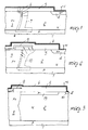
- FIG 1 illustrates a portion of an integrated circuit comprising a junction isolation.
- 1 indicates the substrate with P-type conductivity covered by an N-type epitaxial layer.
- the P+-type region 3 is used for the junction isolation of the epitaxial well or region 2, illustrated in the figure, from the adjacent epitaxial regions, which are not illustrated.
- the well 2 accommodates a layer 4 with N+-type conductivity which belongs to a component of the integrated circuit.
- Said depletion region 7 has been illustrated in the figure in broken lines.
- Figure 2 instead illustrates a known circuit in which the electrostatic shield (field plate) allowing to increase the breakdown voltage is provided.
- a polycrystalline silicon region 9 has been provided inside the oxide layer 5.
- Said region 9 forming a field plate is connected to the ground and has a portion in contact with the isolation region 3 and a region which overlies the junction and is completely embedded in the oxide 5.
- the reference numeral 10 indicates the depletion region around the junction, which as can be seen is altered with respect to the case illustrated in figure 1.
- the region 9 in practice "shields" the effect of the metallization 6, thus increasing the breakdown voltage.
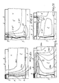
- FIG. 4a and 4b An example of the distribution of the equipotential lines and of the electric field lines with constant modulus for the known solution of figure 2 is illustrated in figures 4a and 4b, from which, as mentioned, it can be seen that the clustering or crowding of the potential lines proximate to the end portion of the shield 9, with a total oxide thickness of approximately 4 »m, induces considerable fields on the surface, causing the breakdown of the junction at a voltage of approximately 300 V (the value of the electric field lines in figure 4b is given in V/cm).
- Figure 3 instead illustrates an example of the solution according to the invention.
- a P ⁇ -type region 15 has been provided which extends along the surface of the body of semiconductor material and more precisely inside the epitaxial well 2 from the isolation region 3 towards the interior of said epitaxial well 2 below the metallization 6.
- Said region 15, together with the shield 9, extends the region on which the potential drop is distributed, thus preventing early breakdown.
- FIGS. 5a and 5b respectively illustrate the distribution of the equipotential lines and of the electric field lines with constant modulus for the solution according to the invention.
- the high-resistivity diffusion 15 allows a more uniform distribution of the potential lines with respect to the similar distributions shown in figures 4a and 4b, and therefore the electric field at the end portion of the polycrystalline-silicon shield 9 decreases considerably.
- the breakdown voltage is therefore raised by a few hundred volts, by virtue of this solution, by appropriately dimensioning the region 9.
- the production of the isolation according to the invention does not require complicated process steps. For example, starting from a P-type substrate, boron is implanted in a known manner to form the lower part of the isolation region 3 (bottom isolation). This is followed by the N-type epitaxial growth (with phosphorus doping), forming the layer 2. A further boron implanting is then performed to provide the upper portion of the isolation (top isolation), followed by a masking to form the extension region 15.
- the P ⁇ implanting of boron (for example with a dose of 3-6x1012cm ⁇ 2, an implanting energy of 70 keV for a length of 50-150 »m) then follows.
- a thermal step is then executed to diffuse the isolation, and then all the other regions of the device, including the silicon oxide layer, the electrostatic shield (field plate) and the metallizations, are produced in a known manner according to the circuit to be obtained.
- the isolation junction can withstand higher voltages, and in particular the surface metallizations passing above the isolation junction can have higher voltages with respect to the case in which only the polycrystalline-silicon electrostatic shield (field plate) is present.
- the described solution is furthermore extremely simple and reliable and requires no complicated process steps, so that the cost of the finished integrated circuit is comparable with that of known devices.
Landscapes
- Element Separation (AREA)
- Semiconductor Integrated Circuits (AREA)
Applications Claiming Priority (2)
| Application Number | Priority Date | Filing Date | Title |
|---|---|---|---|
| IT2034988 | 1988-04-27 | ||
| IT20349/88A IT1217214B (it) | 1988-04-27 | 1988-04-27 | Circuito integrato per alta tensione con isolamento a giunzione |
Publications (3)
| Publication Number | Publication Date |
|---|---|
| EP0339322A2 EP0339322A2 (en) | 1989-11-02 |
| EP0339322A3 EP0339322A3 (en) | 1990-06-13 |
| EP0339322B1 true EP0339322B1 (en) | 1995-12-13 |
Family
ID=11165942
Family Applications (1)
| Application Number | Title | Priority Date | Filing Date |
|---|---|---|---|
| EP89106030A Expired - Lifetime EP0339322B1 (en) | 1988-04-27 | 1989-04-06 | High-voltage integrated circuit with junction isolation |
Country Status (4)
| Country | Link |
|---|---|
| EP (1) | EP0339322B1 (ja) |
| JP (1) | JPH01316971A (ja) |
| DE (1) | DE68925061T2 (ja) |
| IT (1) | IT1217214B (ja) |
Families Citing this family (3)
| Publication number | Priority date | Publication date | Assignee | Title |
|---|---|---|---|---|
| US5426325A (en) * | 1993-08-04 | 1995-06-20 | Siliconix Incorporated | Metal crossover in high voltage IC with graduated doping control |
| US5959342A (en) * | 1993-12-08 | 1999-09-28 | Lucent Technologies Inc. | Semiconductor device having a high voltage termination improvement |
| JP2005236229A (ja) * | 2004-02-23 | 2005-09-02 | Sansha Electric Mfg Co Ltd | 高逆耐圧igbtの構造とその製造方法 |
Citations (1)
| Publication number | Priority date | Publication date | Assignee | Title |
|---|---|---|---|---|
| EP0061551A2 (en) * | 1981-03-28 | 1982-10-06 | Kabushiki Kaisha Toshiba | Planar type semiconductor device with a high breakdown voltage |
Family Cites Families (3)
| Publication number | Priority date | Publication date | Assignee | Title |
|---|---|---|---|---|
| DE2241600A1 (de) * | 1971-08-26 | 1973-03-01 | Dionics Inc | Hochspannungs-p-n-uebergang und seine anwendung in halbleiterschaltelementen, sowie verfahren zu seiner herstellung |
| IT1085486B (it) * | 1977-05-30 | 1985-05-28 | Ates Componenti Elettron | Struttura a semiconduttore integrata monolitica con giunzioni planari schermate da campi elettrostatici esterni |
| NL8401983A (nl) * | 1984-06-22 | 1986-01-16 | Philips Nv | Halfgeleiderinrichting met verhoogde doorslagspanning. |
-
1988
- 1988-04-27 IT IT20349/88A patent/IT1217214B/it active
-
1989
- 1989-04-06 DE DE68925061T patent/DE68925061T2/de not_active Expired - Fee Related
- 1989-04-06 EP EP89106030A patent/EP0339322B1/en not_active Expired - Lifetime
- 1989-04-26 JP JP1107127A patent/JPH01316971A/ja active Pending
Patent Citations (1)
| Publication number | Priority date | Publication date | Assignee | Title |
|---|---|---|---|---|
| EP0061551A2 (en) * | 1981-03-28 | 1982-10-06 | Kabushiki Kaisha Toshiba | Planar type semiconductor device with a high breakdown voltage |
Also Published As
| Publication number | Publication date |
|---|---|
| DE68925061D1 (de) | 1996-01-25 |
| JPH01316971A (ja) | 1989-12-21 |
| IT1217214B (it) | 1990-03-14 |
| IT8820349A0 (it) | 1988-04-27 |
| DE68925061T2 (de) | 1996-05-09 |
| EP0339322A2 (en) | 1989-11-02 |
| EP0339322A3 (en) | 1990-06-13 |
Similar Documents
| Publication | Publication Date | Title |
|---|---|---|
| US5861657A (en) | Graded concentration epitaxial substrate for semiconductor device having resurf diffusion | |
| EP0053854B1 (en) | High voltage semiconductor devices | |
| EP0813250A2 (en) | Trench semiconductor device | |
| EP0632503B1 (en) | Integrated edge structure for high voltage semiconductor devices and related manufacturing process | |
| US6310365B1 (en) | Surface voltage sustaining structure for semiconductor devices having floating voltage terminal | |
| EP0165644B1 (en) | Semiconductor device having an increased breakdown voltage | |
| US20120074458A1 (en) | Quasi-vertical gated npn-pnp esd protection device | |
| US5486718A (en) | High voltage planar edge termination structure and method of making same | |
| US5864167A (en) | Semiconductor device | |
| KR20030005385A (ko) | 전계 효과 트랜지스터의 구조 및 제조 방법 | |
| KR100722012B1 (ko) | 반도체 디바이스 | |
| EP0036319B1 (en) | Semiconductor device | |
| EP0082331B1 (en) | Subsurface avalanche breakdown zener diode | |
| US4892836A (en) | Method for manufacturing semiconductor integrated circuits including CMOS and high-voltage electronic devices | |
| EP0339322B1 (en) | High-voltage integrated circuit with junction isolation | |
| EP0224968B1 (en) | Dielectric passivation | |
| US4125415A (en) | Method of making high voltage semiconductor structure | |
| EP0064614B1 (en) | Improved emitter structure for semiconductor devices | |
| US5959342A (en) | Semiconductor device having a high voltage termination improvement | |
| EP0180315A2 (en) | High breakdown voltage semiconductor device | |
| EP0568692B1 (en) | Power fet with shielded channels | |
| US5324978A (en) | Semiconductor device having an improved breakdown voltage-raising structure | |
| US20030001217A1 (en) | Semiconductor device | |
| EP0780900B1 (en) | Monolithic semiconductor device having an edge structure and method for producing said structure | |
| EP0580256B1 (en) | Semiconductor device for high voltages |
Legal Events
| Date | Code | Title | Description |
|---|---|---|---|
| PUAI | Public reference made under article 153(3) epc to a published international application that has entered the european phase |
Free format text: ORIGINAL CODE: 0009012 |
|
| AK | Designated contracting states |
Kind code of ref document: A2 Designated state(s): DE FR GB NL SE |
|
| PUAL | Search report despatched |
Free format text: ORIGINAL CODE: 0009013 |
|
| AK | Designated contracting states |
Kind code of ref document: A3 Designated state(s): DE FR GB NL SE |
|
| 17P | Request for examination filed |
Effective date: 19901109 |
|
| 17Q | First examination report despatched |
Effective date: 19930427 |
|
| GRAA | (expected) grant |
Free format text: ORIGINAL CODE: 0009210 |
|
| AK | Designated contracting states |
Kind code of ref document: B1 Designated state(s): DE FR GB NL SE |
|
| PG25 | Lapsed in a contracting state [announced via postgrant information from national office to epo] |
Ref country code: NL Free format text: LAPSE BECAUSE OF FAILURE TO SUBMIT A TRANSLATION OF THE DESCRIPTION OR TO PAY THE FEE WITHIN THE PRESCRIBED TIME-LIMIT Effective date: 19951213 |
|
| REF | Corresponds to: |
Ref document number: 68925061 Country of ref document: DE Date of ref document: 19960125 |
|
| PG25 | Lapsed in a contracting state [announced via postgrant information from national office to epo] |
Ref country code: SE Effective date: 19960313 |
|
| ET | Fr: translation filed | ||
| NLV1 | Nl: lapsed or annulled due to failure to fulfill the requirements of art. 29p and 29m of the patents act | ||
| PLBE | No opposition filed within time limit |
Free format text: ORIGINAL CODE: 0009261 |
|
| 26N | No opposition filed | ||
| REG | Reference to a national code |
Ref country code: FR Ref legal event code: D6 |
|
| REG | Reference to a national code |
Ref country code: GB Ref legal event code: IF02 |
|
| PGFP | Annual fee paid to national office [announced via postgrant information from national office to epo] |
Ref country code: GB Payment date: 20020404 Year of fee payment: 14 |
|
| PGFP | Annual fee paid to national office [announced via postgrant information from national office to epo] |
Ref country code: FR Payment date: 20020410 Year of fee payment: 14 Ref country code: DE Payment date: 20020410 Year of fee payment: 14 |
|
| PG25 | Lapsed in a contracting state [announced via postgrant information from national office to epo] |
Ref country code: GB Free format text: LAPSE BECAUSE OF NON-PAYMENT OF DUE FEES Effective date: 20030406 |
|
| PG25 | Lapsed in a contracting state [announced via postgrant information from national office to epo] |
Ref country code: DE Free format text: LAPSE BECAUSE OF NON-PAYMENT OF DUE FEES Effective date: 20031101 |
|
| GBPC | Gb: european patent ceased through non-payment of renewal fee |
Effective date: 20030406 |
|
| PG25 | Lapsed in a contracting state [announced via postgrant information from national office to epo] |
Ref country code: FR Free format text: LAPSE BECAUSE OF NON-PAYMENT OF DUE FEES Effective date: 20031231 |
|
| REG | Reference to a national code |
Ref country code: FR Ref legal event code: ST |