EP0338317B1 - In Direktabbildung und in Bankabbildung wirksamer Informationsprozessor und Verfahren zum Schalten der Abbildungsschemas - Google Patents
In Direktabbildung und in Bankabbildung wirksamer Informationsprozessor und Verfahren zum Schalten der Abbildungsschemas Download PDFInfo
- Publication number
- EP0338317B1 EP0338317B1 EP89105889A EP89105889A EP0338317B1 EP 0338317 B1 EP0338317 B1 EP 0338317B1 EP 89105889 A EP89105889 A EP 89105889A EP 89105889 A EP89105889 A EP 89105889A EP 0338317 B1 EP0338317 B1 EP 0338317B1
- Authority
- EP
- European Patent Office
- Prior art keywords
- address
- memory
- bank
- program
- mapping scheme
- Prior art date
- Legal status (The legal status is an assumption and is not a legal conclusion. Google has not performed a legal analysis and makes no representation as to the accuracy of the status listed.)
- Expired - Lifetime
Links
Images


Classifications
-
- G—PHYSICS
- G06—COMPUTING OR CALCULATING; COUNTING
- G06F—ELECTRIC DIGITAL DATA PROCESSING
- G06F9/00—Arrangements for program control, e.g. control units
- G06F9/06—Arrangements for program control, e.g. control units using stored programs, i.e. using an internal store of processing equipment to receive or retain programs
-
- G—PHYSICS
- G06—COMPUTING OR CALCULATING; COUNTING
- G06F—ELECTRIC DIGITAL DATA PROCESSING
- G06F12/00—Accessing, addressing or allocating within memory systems or architectures
- G06F12/02—Addressing or allocation; Relocation
- G06F12/06—Addressing a physical block of locations, e.g. base addressing, module addressing, memory dedication
- G06F12/0615—Address space extension
- G06F12/0623—Address space extension for memory modules
Definitions
- the present invention relates to an information processing apparatus such as a personal computer, and particularly to an apparatus and method, intended for an information processing apparatus having a plurality of memory blocks each storing a processing program, for mapping the processing programs in the address space of a central processing unit (CPU) based on either direct scheme or bank scheme.
- CPU central processing unit
- Such an information processing apparatus is provided with a ROM-based (ROM : read only memory) program memory for fixedly storing a system program which determines the fundamental operational function of the information processing apparatus.
- the program memory is generally mapped directly in the CPU address space.
- bank scheme as disclosed in, for example, Japanese Patent Unexamined Publication No. 120543/1987 is adopted.
- bank scheme a program memory is formed of multiple memory blocks, with each memory block being mapped on the same address area in the CPU's address space.
- the CPU's address space has an optional area, for storing an application dependent content assigned in proximity to the program area.
- the CPU's address space has an optional area, for storing an application dependent content assigned in proximity to the program area.
- a user wants to load an optional software (program)
- its program memory area is confined in a predetermined address area since the CPU's address space is fixed. Therefore, in order to store the whole of a program which exceeds the limited capacity of the program memory area, it must be mapped on the basis of bank scheme.
- that area can be used as an extended program memory area, and in this case the program memory area can be acquired through the usual direct mapping instead of bank scheme.
- a processor it is desirable for a processor to have the ability of selecting a mapping scheme depending on whether an application involves optional software.
- a recent proposed hardware scheme is capable of selecting either direct or bank mapping for the memory blocks of program memory by use of a jumper wire or hardware switch (or memory switch).
- Information processors with the above-mentioned hardware arrangement have a mapping scheme selected through selective connection by a jumper wire or switch, and have a program memory mounted selectively or replaced from among two kinds of program memories prepared in advance for direct and bank schemes.
- switching of mapping schemes necessitates a hardware modification using a jumper wire or switch, as well as replacement of the program memories for the alternation of software.
- both of these two mapping schemes cannot be accomplished by a single program memory, two types of programs would be required for the two mapping schemes.
- the provision of two kinds of program memories is unfavorable from the viewpoints of working efficiency and maintainability.
- An object of this invention is to provide an improved information processing apparatus which readily deals with both direct scheme and bank scheme.
- Another object of this invention is to provide an information processing apparatus which can deal with both bank scheme and direct scheme by merely switching the mapping schemes on a hardware basis.
- a further object of this invention is to provide an information processing apparatus having a program memory which is in turn conformable with both direct and bank mapping schemes.
- a further object of this invention is to provide a program memory based on the program transition scheme which can deal with both direct and bank mapping schemes.
- a further object of this invention is to provide a program memory based on the program transition scheme which can deal with both direct and bank schemes using only one kind of program.
- a further object of this invention is to provide a program memory based on the program transition scheme which can deal with both direct and bank mapping schemes without program alternation.
- a further object of this invention is to provide a program execution method which can deal with both direct and bank mapping schemes without program memory replacement.
- the information processing apparatus of this invention comprises a program memory for storing a program which can deal with both of bank mapping scheme and direct mapping scheme, and means for selectively setting either direct mapping scheme or bank mapping scheme and mapping the memory address of the program memory in an address space of a central processing unit (CPU) included in the information processing apparatus, in accordance with the selected mapping scheme.
- a program memory for storing a program which can deal with both of bank mapping scheme and direct mapping scheme, and means for selectively setting either direct mapping scheme or bank mapping scheme and mapping the memory address of the program memory in an address space of a central processing unit (CPU) included in the information processing apparatus, in accordance with the selected mapping scheme.
- CPU central processing unit
- the program memory includes a first memory block which stores a first program having the content of processing corresponding to bank mapping scheme, and a second memory block which stores a second program having the content of processing corresponding to direct mapping scheme.
- the second program is substantially the same in the processing content as the first program except for the exclusion of a program for bank switching.
- the program memory includes a third memory block which stores a first processing program, and a fourth memory block which stores a predetermined identification information in a specific memory address and a second processing program.
- the information processing apparatus having the program memory according to the second aspect includes means for, during execution of the first and second processing programs, making decision as to whether the identification information is stored in the address to which the above-mentioned specific memory address corresponds when the fourth memory block is mapped in direct mapping scheme in the CPU's address space in the direct mapping scheme and for implementing the switching of memory banks or the transition of address to be executed in the CPU's address space.
- the second program is executed when the direct mapping scheme is selected, while the first program is executed when the bank mapping scheme is selected.
- the identification information is surely stored in the correspondent address in the CPU's address space when direct mapping scheme is selected, while in bank mapping scheme the identification information is not stored in the correspondent address therein. Accordingly, through the judgement as to whether the identification information is present in the above-mentioned correspondent address, the transition scheme between the first processing program and the second processing program can be selected depending on the mapping scheme. Consequently, the mapping scheme can be switched without replacing the program memory.
- Fig. 1 is a block diagram showing schematically the arrangement of the information processing apparatus which embodies the present invention.
- the inventive information processing apparatus includes a CPU 1 which is the core of the processor for implementing various computational and control operations, and a program memory 4 which is conformable to both direct and bank mappings.
- the CPU 1 has an address space of 1M (20) bytes, for example, and provides the 20-bit address A0 - A19 on an address bus 2.
- the program memory 4 is comprised of a ROM accessible by the 16-bit address MA0 - MA15, i.e., having a capacity of 64K (216) bytes, and it stores, for example, the Basic I/O System (BIOS) that is a control program for input/output units and disk drivers.
- BIOS Basic I/O System
- ROM program memory
- an address decoder 7 which controls enabling and disabling of the output of the ROM 4
- bank registers 5 and 6 and associated address decoders 8 and 9 for designating banks of the ROM 4
- switching circuit 10 which selectively sets direct scheme or bank scheme for mapping the memory area of the ROM 4 in the address space of the CPU 1.
- the address decoders 8 and 9 receive the high-order 6 address bits A14 - A19, for example, provided by the CPU 1 over the address bus 2, and produce an active signal of "1", if the received 6-bit address indicates a location within a predetermined address area and the CPU 1 issues a write signal W.
- the bank registers 5 and 6 are each formed of a D-type flip-flop, for example, having a clock input CK, data input D and data output Q.
- the bank register 5 responds to the active output of the address decoder 8 to latch data D1 on the data bus 3 and to release it as output data through its output terminal Q.
- the bank register 6 responds to the active output of the address decoder 9 to latch data D0 on the data bus 3 and to release it as output data through its output terminal Q.
- the 2 data bits D0 and D1 designate one of four memory blocks (will be mentioned in the below) of the ROM 4.
- the switching circuit 10 includes switches 11, 12 and 13 of hardware implementation for example.
- the switch 11 has an input terminal B receiving the address bit A14 on the address bus 2 and an input terminal C connected to the ground, and delivers its output to the address decoder 7.
- the switch 12 has an input terminal B receiving the Q output of the bank register 5 and an input terminal C connected to a predetermined supply voltage Vcc, and provides its output to the highest address bit MA15 input of the ROM 4.
- the switch 13 has an input terminal B receiving the output Q of the bank register 5 and an input terminal C receiving the address bit A14, and provides its output to the next highest address bit MA14 input of the ROM 4.
- the address decoder 7 receives high-order address bits A15 to A17 from the CPU 1 through the address bus 2 and also receives the output of the switch 11.
- the address decoder 7 produces a "0" signal when the high-order address bits A16 - A19 from the CPU 1 is "C" in hexadecimal or "1100" in binary and the two address bits A14 - A15 are both "0", enabling the ROM 4 to output.
- the reason for setting the address A16 - A19 to the hexadecimal C is that the ROM 4 of the instant embodiment stores, for example, the BIOS mentioned previously and within the segment C000H of CPU 1 is assigned the BIOS area. Accordingly, if the ROM 4 is assigned to other segment of the CPU 1, the address decoder 7 will provide a different value of address bits A16 - A19 for bringing the ROM 4 into the output enabled state.
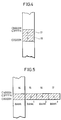
- the ROM 4 has an address space of 0000H-FFFFH (H : hexadecimal) and it is divided into four memory blocks 14, 15, 16 and 17 each having a 16 K (214) byte capacity.
- the first memory block 14 occupies the address area 0000H-3FFFH of ROM 4, the second memory block 15 is assigned to the area 4000H-7FFFH, the third memory block 16 is to the area 8000H-BFFFH, and the fourth memory block 17 is to the area of C000H-FFFFH.
- the first program 100 used in bank mapping is stored in the first and second memory blocks 14 and 15, and the second program used in direct mapping is stored in the third and fourth memory blocks 16 and 17.
- One memory bank is of 16 K bytes in bank mapping.
- first program 100 and second program 200 are virtually the same in the content of process, the first program 100 for bank scheme differs from the second program for direct scheme in the additional inclusion of a bank switching control program for the bank switching between the first memory block 14 and second memory block 15.
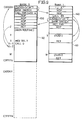
- Fig. 3 shows an example of the first program 100.
- Fig. 3 shows the content of program of the case in which a main routine stored in the first memory block 14 calls a subroutine stored in the second memory block 15.
- the memory bank switching control program is stored in the same address area 110 (hexadecimal 0000-Z of ROM 4 in Fig. 3) of the first and second memory blocks 14 and 15.
- main routine of the first memory block 14 In order for main routine of the first memory block 14 to call a subroutine (SUB1) stored in the second memory block 15, it is appended with instruction MOV BX, Y for transferring starting address y of the subroutine SUB1 relative to the ROM 4 to a register BX (incorporated in the CPU 1), and instruction CALL 0 for invoking the bank switching control program in the first memory block 14.
- the bank switching control program in the memory block 14 includes the bank switching instruction, instruction NOP, and return instruction RET for returning to the main routine.
- the second memory block 15 includes plural kinds of subroutines SUB1 and SUB2, and the bank switching control program.
- the bank switching control program in the second memory block 15 includes the instruction NOP, instruction CALL BX for invoking the content starting at the address stored in register BX (i.e., calling a subroutine), and the bank switching program.
- the operation of the first program will be explained in brief in the following, for the case as an example when the subroutine SUB1 in the second memory block 15 needs to be invoked during execution of the main routine stored in the first memory block 14.
- starting address Y of the subroutine SUB1 is transferred to the register BX.
- the bank switching control program in the first memory block 14 is called by instruction CALL 0, and the memory bank is switched from the first memory block 14 to the second memory block 15 (bank switching operation will be explained later).
- the subroutine SUB1 beginning at address Y is called by instruction CALL BX in the bank switching control program in the second memory block 15, and it is executed.
- the RET instruction transfers control back to the bank switching control program in the second memory block 15 so that the bank is switched from the second memory block 15 to the first memory block 14. Subsequently, the RET instruction of the bank switching control program in the first memory block 14 brings the process back to the main routine.
- address W is transferred to the register BX at address X of the main routine.
- the address area 110 shown in Fig. 3 is extended so that the bank switching control program from the second memory block 15 to the first memory block 14 is stored in the extended area.
- the address decoder 7 receives address bits A16 - A19 and A15 and the "0" bit from the switch 11. The address decoder 7 enables the ROM 4 to output only when the address bit A15 is "0" and the address bits A16 - A19 are equal to hexadecimal C. Accordingly, the contents of ROM 4 are mapped in the address space C0000H-C7FFFH where the address bit A15 is "0" in the segment C of CPU 1. Since the ROM 4 has its most significant address bit MA15 fixed to "1", it has the address area of 80000H-FFFFH be accessible. Consequently, as shown in Fig. 4, the third and fourth memory blocks 16 and 17, i.e., the second program 200, are mapped directly to the address area of C0000H-C7FFFH of CPU 1.
- the ROM 4 With all input terminals of the switches 11 - 13 in the switching circuit 10 being set to the B-input position, the ROM 4 has its address bits MA15 and MA14 receive the outputs of the bank registers 5 and 6, respectively, and the address decoder 7 receives directly the address bits A14 and A15 from the CPU 1. Consequently, as shown in Fig. 5, the first through fourth memory blocks 14 - 17 of ROM 4 are mapped as memory banks 0 - 3 in the address area C0000H-C3FFFH, where the address bits A14 and A15 are both "0", in the address area C0000H-CFFFH of the CPU 1.
- the memory blocks of ROM 4 are selected by the most significant address bits MA14 and A15 provided by the bank registers 5 and 6, i.e., 2-bit data DO and D1 from the CPU 1.
- data (D1, DO) being (0, 0)
- the first memory block (bank 0) 14 is designated, with (0, 0)
- the second memory block (bank 1) 15 is designated, with (1, 0)
- the third memory block (bank 2) 16 is designated, and with (1, 1), the fourth memory block (bank 3) is designated.
- bank switching is carried out by the CPU 1 which sets the bank designation data D0 and D1 to the bank registers 5 and 6 in accordance with the bank switching control program included in the first program 100. More specifically, the bank switching takes place as follows. In the bank designation, the CPU 1 places the bank designation data D0 and D1 on the data bus 3, and thereafter issues a set of predetermined values of address bits A14 - A19 (e.g., 110000) to the address decoders 8 and 9 and further issues the write signal W thereto. The address decoders 8 and 9 respond to the address bits A14-A19 and the write signal W to provide an active signal to the clock input CK of the bank registers 5 and 6.
- a set of predetermined values of address bits A14 - A19 e.g., 110000
- the bank registers 5 and 6 latch the data on the data bus 3.
- the values of address which causes the address decoders 8 and 9 to produce active signals should be set so that the decoders 8 and 9 respond only when a memory bank within address range C0000H-C3FFFH is accessed, thereby avoiding possible unnecessary rewriting of the bank registers 5 and 6.
- the bank registers 5 and 6 are both initialized to have Q output "1" when power is turned on, and therefore the fourth memory block (bank 3) 17 is selected as the memory bank initially. Consequently, the bank switch command to the first memory block 14 is stored in address COOOH (relative to ROM 4) of the fourth memory block 17. By this bank switching command, the bank is switched to the first memory block (memory bank 0) 14 under control of the CPU 1, followed by the execution of the initialization routine and then the prescribed process by the first program which has been mapped as bank 0 and bank 1. It should be noted that address C000H of the fourth memory block (memory bank 3) 17 is unnecessary at the execution of the second processing program 200, and on this account the second program 200 is designed so that the address C000H is not used at the execution of the second program 200.
- a single ROM is used as the program memory 4, in which the first and second programs are stored.
- the first and second programs may be stored in separate ROMs, and furthermore each memory block may be arranged in each individual ROM.
- the information processing apparatus includes a CPU 1, a program memory 40, a bank register 70, address decoders 80 and 90, and a switching circuit 105.
- the CPU 1 has an address space of 1 M bytes (20 bytes) ranging 00000H-FFFFFH, for example, and provides 20-bit address A0 - A19 on the address bus 2.
- the program memory 40 is arranged in a 32 X(215) byte ROM, including a first memory block 50 of 16 K bytes ranging 0000H-3FFFH and a second memory block 60 of 16 K bytes ranging 4000H-7FFFH, as shown schematically in Fig. 7.
- the first memory block 50 stores the first processing program
- the second memory block 60 stores the second processing program.
- the first and second processing programs in unison form a control program such as BIOS.
- the address decoder 80 serves to decode the high-order 6 address bits A14 - A19, for example, on the address bus 2, and only when the given address is within a predetermined area, it provides an active signal to the clock input CK of the bank register 70 in response to the write signal W.
- the bank register 70 responds to the active input at its clock input CK to latch the bank designation data D0 on the data bus 3 and to release the latched data as output Q.
- the switching circuit 105 selects either direct scheme or bank scheme as a scheme for mapping the contents of program memory 40 in the address space of CPU 1.
- the switching circuit 105 includes switches 111 and 112.
- the switch 111 has an input terminal B receiving an address bit A14 from the CPU 1 and an input terminal C connected to the ground, while the switch 112 has an input terminal B receiving the Q output from the bank register 70 and an input terminal C receiving the address bit A14 from the CPU 1.
- the address decoder 90 receives 5 address bits A15-A19 from the CPU 1 and the output of the switch 111, and delivers its output to the output enable terminal OE ⁇ of the program memory 40.
- the address decoder 90 produces an active enable signal ("0" level in Fig. 6) only when the address A16 - A19 from the CPU 1 is hexadecimal C, for example, and at the same time the address bit A15 and the output of switch 111 are both "0".
- the program memory 40 has its address designated by the output of the switch 112 and the address A0 - A13 from the CPU 1. The output of the switch 112 is given to the most significant address bit MA14 of the program memory 40.
- the bank mapping scheme is selected by setting the input terminals of the switches 111 and 112 to the respective B input position.
- the contents of the program memory 40 are mapped as a memory bank in the address area in which the address A16 - A19 is hexadecimal C and address bits A14 and A15 are both "0", i.e., in the area C0000H-C3FFFH of CPU address space.
- the most significant address bit MA14 of the program memory 40 When the most significant address bit MA14 of the program memory 40 is "0", the first memory block 50 in the address area 0000H-3FFFH of the program memory 40 is selected as bank 0, and when the most significant address bit MA14 is "1", the second memory block 60 in the address area 4000H-7FFFH of the program memory 40 is selected as bank 1.
- direct mapping scheme is selected.
- the whole contents of program memory 40 i.e., the first and second memory blocks 50 and 60
- the address bit A14 of CPU 1 is supplied to the most significant address bit MA14 of the program memory 40 through the switch 112, and the first memory block 50 is mapped in the address area COOOOH-3FFFFH of CPU 1, and the second memory block 60 is mapped in the address area C4000H-C7FFFH of CPU 1.
- the first and second processing programs stored in the first memory block 50 and second memory block 60, respectively, is designed to have the contents as shown specifically for example in Fig. 8 and 9, so that both of direct scheme and bank scheme can be compatibly used. Shown in Figs. 8 and 9 are examples in which the main routine of the first processing program invokes the subroutines of the second processing program.
- the first and second memory blocks 50 and 60 store the first and second control programs 130 and 140 in the respective starting addresses 0000H and 4000H through a relative address Z.
- Mapping scheme identification information "JA" is stored in the specific address (4000H in Figs. 8 and 9) of the second memory block 60.
- the "CALL FAR C400 : 4" instruction is to call and execute the contents beginning at the address C4004H which is the starting address C4000H added by the offset address 4.
- the "RET FAR” instruction is to shift the execution address (address to be executed) to the address next to the address where the "CALL FAR” instruction is stored.
- the instructions “CALL FAR C400 : 4" and "RET FAR” are to merely shift the execution address in the address space of CPU 1 in the direct mapping scheme.
- Figs. 8 and 9 the operation in the case in which the main routine in the first processing program calls a subroutine in the second processing program to execute it.
- the addresses X, Y, Z and W represent offset addresses from the starting address C0000H or C40000H of each segment (each memory block). Arrows in the figures indicates the progression of operation.
- the first and second control programs are stored with their addresses being correspondent mutually so that the address counter does not be revised unnecessary at each instruction execution.
- the operation in direct mapping scheme will first be explained with reference to Fig. 8.
- the first memory block 50 is mapped in CPU's address space C0000H-C3FFFH
- the second memory block 60 is mapped in C4000H-C7FFFH thereof. Accordingly, the identification information "JA" is stored in the specific address C4000H of the CPU's address space.
- the starting address Y of the subroutine SUB1 is transferred to the register BX (incorporated in CPU 1).
- the first control program 130 is executed by the instruction "CALL 0".
- the command at the top address C0000H of the first control program 130 decides whether or not the identification information "JA" is stored in address C4000H of CPU 1.
- the decision result is "yes" in this direct mapping scheme. Accordingly, the bank switching instruction stored in the next address is skipped.
- the instruction "CALL FAR C400 : 4" at the skipped destination address causes the execution program to make transition from the first processing program to the second processing program, and then the instruction "CALL BX" at address C4004H is executed as shown by the arrow in Fig. 8.
- the register BX is already supplied with the starting address Y of the subroutine SUB1 by the main routine of the first processing program. Then, the subroutine SUB1 is invoked by the CALL instruction and it is executed. On completion of execution of the subroutine SUB1, the RET instruction in the subroutine SUB1 causes the execution address to move to the decision step of identification information in the second processing program.
- the RET FAR instruction is executed, and the program sequence returns to the first control program 130. Namely, the execution program makes a transition from the second processing program to the first processing program. Subsequently, through the execution of the RET instruction in the first control program 130, the sequence returns to the main routine of the first processing program. It should be noted that if it is intended to call and execute the subroutine SUB2 from the main routine, the subroutine starting address W is stored in the register BX.
- the switches 111 and 112 have their input terminals set to the B input position. Consequently, the first and second memory blocks 50 and 60 are mapped as bank 0 and bank 1 in the address area C0000H-C3FFFH in the address space of CPU 1. Accordingly, the identification information "JA" is not stored in the specific address C4000H of CPU 1. Therefore, when the main routine of the first processing program has invoked the first control program 130, the decision step for identification information results in "no", and the bank switching instruction is executed.
- the bank switching instruction sets the bank register 70 to store "1" under control of CPU 1, and the memory bank is switched from bank 0 to bank 1, followed by the transition from the first processing program to the second processing program.
- the CALL BX instruction in the second control program 140 of the second processing program calls and executes the subroutine SUB1 beginning at the address Y stored in the register BX.
- the RET instruction in the subroutine SUB1 brings the program sequence back to the second control program 140.
- Return to the second control program 140 is immediately followed by the decision on identification information.
- the decision result is "no" in this case, and the bank switching instruction stored in the next address is executed.
- the bank switching takes place in the manner of setting in the bank register 70 "0" under control of CPU 1.
- the transition from the second processing program to the fist processing program is carried out, and then the first control program 130 is executed.
- the RET instruction in the first control program 130 brings the program sequence back to the main routine of the first processing program, and the execution of main routine is resumed at address X + 2.
- mapping schemes are readily accomplished by switching the input terminals of the switches 111 and 112 in the switching circuit 105.
- the second and first control programs are added to the first and second control programs as shown in Figs. 8 and 9, respectively.
- Any decoder configuration may be employed as far as the following requirement is satisfied.
- one is designed to produce an active enable signal when the address A16 - A19 is hexadecimal C and at the same time the address bit A15 is "0" (address bit A14 may be any), and the other is to produce an active enable signal when the address A16 - A19 is hexadecimal C and at the same time address bits A14 and A15 both are "0".
- each processing program may be stored in two or more ROMs.
- each processing program may be stored in two or more ROMs.
- replacing the most significant address bits MA14 of ROM 40 in Fig. 6 with the chip enable signal CE ⁇ allows each memory block to be readily mapped in any of bank mapping scheme and direct mapping scheme.
- the structure may be also employed in which the output of the switch 112 and the output of the address decoder 90 in Fig. 6 is subjected to such a logical operation as OR or NOR corresponding to each memory block and then applied to the output enable terminal of ROM.
- each ROM has its number of address bits decreased as the number of ROMs increases, and, by logically processing the remaining address bits from the CPU 1 appropriately, the ROM memory blocks can readily be mapped in the address space of CPU 1 according to each mapping scheme.
- a program which is designed to deal with both of the bank and direct schemes is stored in the program memory, and therefore the information processing apparatus can deal with any of the direct mapping scheme and bank mapping scheme by merely switching the mapping scheme on a hardware basis, instead of replacing the program memory.
Landscapes
- Engineering & Computer Science (AREA)
- Theoretical Computer Science (AREA)
- Physics & Mathematics (AREA)
- General Engineering & Computer Science (AREA)
- General Physics & Mathematics (AREA)
- Software Systems (AREA)
- Stored Programmes (AREA)
- Executing Machine-Instructions (AREA)
Claims (15)
- Informationsprozessor mit einer zentralen Prozessoreinheit (1) mit einem vorbestimmten Adressenraum, mit:Speichermitteln (4) mit einem ersten Speicherblock (14, 15), der aus einer Anzahl von Speicherblocks zum speichern eines ersten Speicherprogramms (100) gebildet ist, und einem zweiten Speicherblock, der aus wenigstens einem Speicherblock zum Speichern eines zweiten Speicherprogramms (200) gebildet ist, wobei das erste Programm bezüglich des Bearbeitungsinhalts im wesentlichen das Gleiche wie das zweite Programm ist, mit Ausnahme, daß das erste Programm ein Steuerprogramm (110) zum Schalten der Speicherbereiche hat;Mitteln zum wahlweisen bezeichnen entweder der direkten Abbildung oder der Bereichsabbildung als einem Abbildungsschema zum Abbilden der Speicherblocks der Speichermittel in dem vorbestimmten Adressenraum; und Mitteln (5, 6, 7, 8, 9, 11, 12, 13) zum Schalten der Speichermittel in dem Adressenraum gemäß einem Abbildungsschema, welches von den Bezeichnungsmitteln bezeichnet worden ist;wobei die Schaltmittel jede der Anzahl Speicherblocks im ersten Speicherblock als einen Speicherbereich im selben Adressenbereich des Adressenraums abbilden, wenn das Bereichsabbildungsschema bezeichnet ist, so daß das erste Programm durchgeführt wird, und der zweite Speicherblock in eins-zu-eins-Entsprechung in dem Adressenraum abgebildet wird, wenn das direkt Abbildungsschema bezeichnet ist, so daß das zweite Programm durchgeführt wird.
- Prozessor nach Anspruch 1, wobei die Speichermittel einen einzigen Festspeicher aufweisen.
- Prozessor nach Anspruch 1, wobei die Schaltmittel aufweisenMittel (5, 6, 8, 9, 12, 13) zum Bezeichnen eines zugänglichen Speicherbereichs der Speichermittel gemäß dem Abbildungsschema, das von den Bezeichnungsmitteln bezeichnet worden ist, undMittel (7, 11) zum Einstellen eines Adressenbereichs im Adressenraum, in welchem der Speicherbereich, welcher von den Bezeichnungsmitteln bezeichnet worden ist, abgebildet ist.
- Prozessor nach Anspruch 3, wobei die Adressenbereichs-Einstellmittel Ausgangssteuerungsmittel (7, 11) aufweisen, um die Speichermittel in einen eine Ausgabe ermöglichenden Zustand zu bringen, und zwar in Übereinstimmung mit einer vorbestimmten Anzahl von höherwertigen Bits (A14 - A19) aus der Adresse, die von der zentralen Prozessoreinheit abgeleitet sind, und dem Abbildungsschema, welches von den Bezeichnungsmitteln bezeichnet ist, wobei die Ausgangssteuermittel den Ausgang der Speichermittel nur dann ermöglichen, wenn die Adresse, welche von der zentralen Prozessoreinheit geliefert worden ist, eine Adresse in dem Adressenbereich des Adressenraums repräsentiert, der den Speichermitteln in Abhängigkeit von dem aus dem Bereichs- und Direkt-Abbildungsschema bezeichneten Abbildungsschema zugeordnet ist.
- Prozessor nach Anspruch 4, wobei die Ausgangssteuermittel aufweisenerste Wählmittel (11) zum Wählen entweder einen vorbestimmten Binärwertes oder eines vorbestimmten Adressenbits aus den höherwertigen Adressenbits, gemäß dem Abbildungsschema, das von den Bezeichnungsmitteln bezeichnet ist, undDekodermittel (7) zum Dekodieren der verbleibenden Adressenbits aus den höherwertigen Adressenbits und dem Ausgang der ersten Wählmittel und Steuern des Ausgangmöglich-Zustandes der Speichermittel in Abhängigkeit von dem dekodierten Ergebnis.
- Prozessor nach Anspruch 3, wobei die Bezeichnungsmittel Registermittel (5, 6) aufweisen zum Speichern von Daten, welche einen Speicherbereich unter der Vielzahl von Speicherbereichen bezeichnen, und Bezeichnungssteuermittel (12, 13) zum Einstellen eines zugänglichen Speicherbereiches in den Speichermitteln in Übereinstimmung mit dem Bereich, der Daten bezeichnet, die in den Registermitteln gespeichert sind, und dem Abbildungsschema, das durch die Bezeichnungsmittel bezeichnet worden ist;wobei die Bezeichnungssteuermittel den zugänglichen Speicherbereich der Speichermittel so einstellen, daß nur ein Speicherbereich, der durch die bereichsbezeichneten Daten bezeichnet ist, zugänglich ist, wenn das Bereichsabbildungsschema bezeichnet ist, und den zugänglichen Adressenbereich der Speichermittel so einstellen, daß eine derartige zentrale Prozessoreinheit zum ganzen zweiten Speicherblock, der das zweite Programm speichert, den Zugriff durchführen kann, wenn das Direktabbildungsschema bezeichnet ist.
- Prozessor nach Anspruch 6, wobei die Registermittel eine Anzahl von Datenzwischenspeichern (5, 6) aufweisen und weiterhin die Bezeichnungssteuermittel zweite Wählmittel (12) zum Wählen entweder eines zwischengespeicherten Datums in einem vorbestimmten Datenzwischenspeicher aus der Vielzahl von Datenzwischenspeichern oder eines vorbestimmten Binärwertes in Übereinstimmung mit dem bezeichneten Abbildungsschema, aufweisen und zum Zuführen des gewählten an einen Adresseneingang der Speichermittel, und dritte Wählmittel (13) zum Wählen entweder eines zwischengespeicherten Datums in dem verbleibenden Datenzwischenspeicher oder eines vorbestimmten Adressenbits aus den Adressenbits, die von der zentralen Prozessoreinheit zugeführt worden sind, in Abhängigkeit von dem bezeichneten Abbildungsschema, und Zuführen des gewählten an einen Adresseneingang der Speichermittel.
- Informationsprozessor mit einer zentralen Prozessoreinheit (1) mit einem vorbestimmten Adressenraum, mit:Speichermitteln (40) mit einem ersten Speicherblock (50) zum Speichern eines ersten Bearbeitungsprogramms, und einem zweiten Speicherblock zum Speichern eines zweiten Bearbeitungsprogramms, wobei der zweite Speicherblock eine vorbestimmte Identifikationsinformation an einem vorbestimmten Speicherort speichert;Mitteln (105) zum wahlweisen Bezeichnen entweder des Direktabbildungsschemas oder des Bereichsabbildungsschemas als Abbildungsschema zum Abbilden des der Speicherblocks der Speichermittel in dem Adressenraum;Mitteln (70, 80, 90, 111, 112) zum Schalten der Abbildungs-schemata für die Speichermittel in Übereinstimmung mit dem bezeichneten Abbildungsschema, wobei die Schaltmittel die ersten und zweiten Speicherblocks jeweils als einen Speicherbereich auf demselben Adressenbereich in dem Adressenraum abbilden, wenn das Bereichsabildungsschema gewählt ist, und die ersten und zweiten Speicherblocks in 1:1-Entsprechung in dem Adressenraum abbilden, wenn das Direktabbildungsschema gewählt ist;Mitteln (1) zum Entscheiden während der Durchführung des ersten und zweiten Bearbeitungsprogramms, ob die Identifikationsinformation an einer Adresse im Adressenraum entsprechend dem vorbestimmten Speicherort gespeichert ist, wenn der zweite Speicherblock in dem Adressenraum bei Direktabbildungsschema abgebildet ist; und Steuermitteln (1) zum Schalten der Speicherbereiche von einem Speicherbereich, in dem das in Durchführung befindliche Bearbeitungsprogramm gespeichert ist, in den anderen Speicherbereich, wenn das Entscheidungsergebnis der Entscheidungsmittel die Abwesenheit der Identifikationsinformation angibt, und zum Schieben einer Adresse in eine Adresse, die als nächstes in dem zweiten Bearbeitungsprogramm in dem Adressenraum durchgeführt werden soll, ohne daß der Bereich umgeschaltet wird, wenn das Entscheidungsergebnis der Entscheidungsmittel die Anwesenheit der Identifikationsinformation angibt.
- Prozessor nach Anspruch 8, wobei die Speichermittel einen einzigen Festspeicher aufweisen.
- Prozessor nach Anspruch 8, wobei die Schaltmittel aufweisen:Mittel (70, 80, 112) zum Definieren eines zugänglichen Adressenbereiches der Speichermittel in Abhängigkeit von dem Abbildungsschema, welches durch die Bezeichnungsmittel bezeichnet worden ist; und Mitteln (90, 111) zum Einstellen eines Adressenbereiches in dem Adressenraum, in welchem der Speicherbereich, welcher durch die Bezeichnungsmittel bezeichnet worden ist, abgebildet ist, in Abhängigkeit von dem Abbildungsschema, welches durch die Bezeichnungsmittel bezeichnet worden ist.
- Prozessor nach Anspruch 10, wobei die Einstellmittel aufweisen Ausgangssteuermittel (90, 111) zum Ermöglichen des Ausgangs an den Speichermitteln, basierend auf hochwertigen Adressenbits (A14 - A19) von einer Adresse, die von der zentralen Prozessoreinheit geliefert worden ist, und dem Abbildungsschema, welches durch die Bezeichnungsmittel bezeichnet worden ist,wobei die Ausgangssteuermittel die Speichermittel nur dann in den, einen Ausgang ermöglichenden Zustand bringen, wenn die Adresse von der zentralen Prozessoreinheit einen Ort in dem Adressenbereich des Adressenraums representiert, der für die den Speichermittel entsprechend jedem Abbildungsschema von Direkt- und Bereichsabbildungsschema, bezeichnet ist.
- Prozessor nach Anspruch 11, wobei die Ausgangssteuermittel aufweisen:erste Wählmittel (111) zum Wählen und Zuführen entweder eines vorbestimmten Binärwertes oder eines vorbestimmten Adressenbits aus den höherwertigen Adressenbits, in Abhängigkeit von dem Abbildungsschema, das von den Bezeichnungsmitteln bezeichnet worden ist, undDekodermittel (70) zum Dekodieren der empfangenen verbleibenden Adressenbits der hochwertigen Adressenbits und des Ausgangs der ersten Wählmittel und zum Steuern der Möglichkeit des Ausgangs an den Speichermitteln in Abhängigkeit von dem dekodierten Ergebnis.
- Prozessor nach Anspruch 10, wobei die Speicherbereichs-Bezeichnungsmittel aufweisen:Registermittel (70) zum Speichern der Daten zum Bezeichnen eines Speicherbereichs,Bezeichnungssteuermittel (112) zum Einstellen eines zugänglichen Speicherbereiches der Speichermittel in Übereinstimmung mit den bereichsbezeichnenden Daten, die in den Registermitteln gespeichert sind und dem Abbildungsschema, das durch die Bezeichnungsmittel bezeichnet worden ist,wobei die Bezeichnungssteuermittel den zugänglichen Speicherbereich der Speichermittel so bezeichnen, daß nur der von den Bereichsbezeichnungsdaten bezeichnete Speicherbereich zugänglich ist, wenn das Bereichsabbildungsschema bezeichnet ist, und der zugängliche Speicherbereich der Speichermittel so bezeichnet ist, daß die zentrale Prozessoreinheit insgesamt zu den ersten und zweiten Speicherblocks Zugriff erlangen kann, um das erste und zweite Bearbeitungsprogramm zu speichern, wenn das Direktabbildungsschema bezeichnet ist, und wobei weiterhindie Steuermittel (1) Mittel (1) zum Einschreiben der Bankbezeichnungsdaten in die Registermittel in Abhängigkeit von der entschiedenen Abwesenheit der Identifikationsinformation bei der Entscheidung der Entscheidungsmittel.
- Prozessor nach Anspruch 13, wobei die Registermittel einen Datenzwischenspeicher (70) aufweisen und die Bezeichnungssteuermittel zweite Wählmittel (112) aufweisen, um wahlweise einem Adresseneingang der Speichermittel entweder ein zwischengespeichertes Datum in dem Datenzwischenspeicher oder ein vorbestimmtes Adressenbit aus der Adresse von der zentralen Prozessoreinheit zuführen, und zwar in Abhängigkeit von den bezeichneten Abbildungsschema.
- Prozessor nach Anspruch 8, wobei jedes der ersten und zweiten Bearbeitungsprogramme ein Steuerprogramm (130, 140) aufweist, um zu entscheiden, ob die Identifikationsinformation in der Adresse gespeichert ist, welche dem vorbestimmten Speicherort entspricht, wenn die ersten und zweiten Speicherblocks in dem Adressenraum abgebildet werden, basierend auf dem Direktabbildungsschema, und zum Ausführen des Speicherbereichs-Umschaltens in Abhängigkeit von der entschiedenen Abwesenheit dieser Information und zum Schieben einer Adresse in eine Adresse, die als nächstes ausgeführt werden soll, in dem Adressenraum ohne Bereichsumschaltung, in Abhängigkeit von der entschiedenen Anwesenheit der Identifikationsinformation.
Applications Claiming Priority (4)
| Application Number | Priority Date | Filing Date | Title |
|---|---|---|---|
| JP97305/88 | 1988-04-20 | ||
| JP63097305A JPH01267751A (ja) | 1988-04-20 | 1988-04-20 | プログラム遷移方式 |
| JP146306/88 | 1988-06-14 | ||
| JP63146306A JPH0752408B2 (ja) | 1988-06-14 | 1988-06-14 | 情報処理装置 |
Publications (3)
| Publication Number | Publication Date |
|---|---|
| EP0338317A2 EP0338317A2 (de) | 1989-10-25 |
| EP0338317A3 EP0338317A3 (en) | 1990-10-10 |
| EP0338317B1 true EP0338317B1 (de) | 1996-01-10 |
Family
ID=26438491
Family Applications (1)
| Application Number | Title | Priority Date | Filing Date |
|---|---|---|---|
| EP89105889A Expired - Lifetime EP0338317B1 (de) | 1988-04-20 | 1989-04-04 | In Direktabbildung und in Bankabbildung wirksamer Informationsprozessor und Verfahren zum Schalten der Abbildungsschemas |
Country Status (5)
| Country | Link |
|---|---|
| US (1) | US5127096A (de) |
| EP (1) | EP0338317B1 (de) |
| KR (1) | KR920006615B1 (de) |
| CN (1) | CN1016652B (de) |
| DE (1) | DE68925376T2 (de) |
Families Citing this family (12)
| Publication number | Priority date | Publication date | Assignee | Title |
|---|---|---|---|---|
| US5146581A (en) * | 1988-02-24 | 1992-09-08 | Sanyo Electric Co., Ltd. | Subprogram executing data processing system having bank switching control storing in the same address area in each of memory banks |
| US5349680A (en) * | 1990-11-07 | 1994-09-20 | Kabushiki Kaisha Toshiba | Information processing apparatus for executing application programs under control of a system program |
| JP2648768B2 (ja) * | 1991-03-25 | 1997-09-03 | 株式会社椿本チエイン | シーケンス制御動作モードと他の動作モードとの切換変更方法 |
| EP0596198B1 (de) * | 1992-07-10 | 2000-03-29 | Sony Corporation | Flash-EPROM mit Löschprüfung und Architektur zum Adresszerhacken |
| AU710489B2 (en) * | 1995-04-28 | 1999-09-23 | Nec Corporation | Paging receiver employing memory banking system |
| US5802544A (en) * | 1995-06-07 | 1998-09-01 | International Business Machines Corporation | Addressing multiple removable memory modules by remapping slot addresses |
| US5867719A (en) * | 1996-06-10 | 1999-02-02 | Motorola, Inc. | Method and apparatus for testing on-chip memory on a microcontroller |
| US5901103A (en) * | 1997-04-07 | 1999-05-04 | Motorola, Inc. | Integrated circuit having standby control for memory and method thereof |
| DE19720990A1 (de) * | 1997-05-20 | 1998-11-26 | Alsthom Cge Alcatel | Programmgesteuerte Einrichtung mit Nachlademöglichkeit für und Umschaltemöglichkeit auf zweites Betriebssystem ohne Programmunterbrechung |
| US7127718B1 (en) * | 2000-11-15 | 2006-10-24 | National Semiconductor Corporation | Multitasking microcontroller for controlling the physical layer of a network interface card and method of operation |
| US20130132704A1 (en) * | 2010-09-10 | 2013-05-23 | Rambus Inc. | Memory controller and method for tuned address mapping |
| US8914615B2 (en) | 2011-12-02 | 2014-12-16 | Arm Limited | Mapping same logical register specifier for different instruction sets with divergent association to architectural register file using common address format |
Family Cites Families (10)
| Publication number | Priority date | Publication date | Assignee | Title |
|---|---|---|---|---|
| US4300192A (en) * | 1974-04-18 | 1981-11-10 | Honeywell Information Systems Inc. | Method and means for storing and accessing information in a shared access multiprogrammed data processing system |
| GB1483442A (en) * | 1975-10-09 | 1977-08-17 | Standard Telephones Cables Ltd | Computing machine including a directly addressable memory arrangement |
| US4340932A (en) * | 1978-05-17 | 1982-07-20 | Harris Corporation | Dual mapping memory expansion unit |
| US4316244A (en) * | 1978-11-08 | 1982-02-16 | Data General Corporation | Memory apparatus for digital computer system |
| JPS57185551A (en) * | 1981-05-08 | 1982-11-15 | Sharp Corp | Data access system of memory bank in microcomputer system |
| US4475176A (en) * | 1981-08-06 | 1984-10-02 | Tokyo Shibaura Denki Kabushiki Kaisha | Memory control system |
| US4403287A (en) * | 1981-08-24 | 1983-09-06 | Bell Telephone Laboratories, Incorporated | Microprocessor architecture having internal access means |
| US4485457A (en) * | 1983-05-31 | 1984-11-27 | Cbs Inc. | Memory system including RAM and page switchable ROM |
| US4761733A (en) * | 1985-03-11 | 1988-08-02 | Celerity Computing | Direct-execution microprogrammable microprocessor system |
| JPS62120543A (ja) * | 1985-11-20 | 1987-06-01 | Fujitsu Ltd | メモリバンクの切替方式 |
-
1989
- 1989-04-04 DE DE68925376T patent/DE68925376T2/de not_active Expired - Fee Related
- 1989-04-04 EP EP89105889A patent/EP0338317B1/de not_active Expired - Lifetime
- 1989-04-07 US US07/334,498 patent/US5127096A/en not_active Expired - Fee Related
- 1989-04-20 CN CN89103203A patent/CN1016652B/zh not_active Expired
- 1989-04-20 KR KR1019890005286A patent/KR920006615B1/ko not_active Expired
Also Published As
| Publication number | Publication date |
|---|---|
| CN1016652B (zh) | 1992-05-13 |
| US5127096A (en) | 1992-06-30 |
| EP0338317A2 (de) | 1989-10-25 |
| DE68925376T2 (de) | 1996-09-05 |
| KR920006615B1 (ko) | 1992-08-10 |
| KR890016467A (ko) | 1989-11-29 |
| DE68925376D1 (de) | 1996-02-22 |
| EP0338317A3 (en) | 1990-10-10 |
| CN1037416A (zh) | 1989-11-22 |
Similar Documents
| Publication | Publication Date | Title |
|---|---|---|
| US4679140A (en) | Data processor with control of the significant bit lengths of general purpose registers | |
| JP3683230B2 (ja) | データ処理装置、命令セット切換方法、データ処理アーキテクチャおよびデータ処理装置作動方法 | |
| US4361868A (en) | Device for increasing the length of a logic computer address | |
| EP0007028B1 (de) | Externe Speichereinrichtung mit Basisregister | |
| EP0476722B1 (de) | Datenverarbeitungssystem | |
| US4382278A (en) | Hierarchial memory system with microcommand memory and pointer register mapping virtual CPU registers in workspace cache #4 and main memory cache | |
| US5249280A (en) | Microcomputer having a memory bank switching apparatus for accessing a selected memory bank in an external memory | |
| EP0248436A2 (de) | Verfahren und Vorrichtung zur Datenverarbeitung | |
| JPS6114535B2 (de) | ||
| EP0330226B1 (de) | Vorrichtung und Verfahren zur Ausführung eines Unterprogramms in einem Datenverarbeitungssystem mit Blockumschaltung | |
| EP0338317B1 (de) | In Direktabbildung und in Bankabbildung wirksamer Informationsprozessor und Verfahren zum Schalten der Abbildungsschemas | |
| US5283889A (en) | Hardware based interface for mode switching to access memory above one megabyte | |
| US4223381A (en) | Lookahead memory address control system | |
| US4491908A (en) | Microprogrammed control of extended integer and commercial instruction processor instructions through use of a data type field in a central processor unit | |
| EP0315139B1 (de) | Mikroprozessor | |
| JP4988082B2 (ja) | マイクロプロセッサ及びデータ処理システム | |
| KR100287600B1 (ko) | 확장가능한레지스터를제공하는데이타처리시스템및그방법 | |
| US4314332A (en) | Memory control system | |
| US6321332B1 (en) | Flexible control of access to basic input/output system memory | |
| US5664169A (en) | Microprogrammable processor capable of accessing unused portions of control store as fast data memory | |
| KR100960095B1 (ko) | 마이크로컨트롤러 명령어 셋트 | |
| US6321319B2 (en) | Computer system for allowing a two word jump instruction to be executed in the same number of cycles as a single word jump instruction | |
| US20020004877A1 (en) | Method and system for updating user memory in emulator systems | |
| JPS6362778B2 (de) | ||
| JP2954988B2 (ja) | 情報処理装置 |
Legal Events
| Date | Code | Title | Description |
|---|---|---|---|
| PUAI | Public reference made under article 153(3) epc to a published international application that has entered the european phase |
Free format text: ORIGINAL CODE: 0009012 |
|
| AK | Designated contracting states |
Kind code of ref document: A2 Designated state(s): DE FR GB |
|
| PUAL | Search report despatched |
Free format text: ORIGINAL CODE: 0009013 |
|
| AK | Designated contracting states |
Kind code of ref document: A3 Designated state(s): DE FR GB |
|
| 17P | Request for examination filed |
Effective date: 19901016 |
|
| 17Q | First examination report despatched |
Effective date: 19930521 |
|
| GRAA | (expected) grant |
Free format text: ORIGINAL CODE: 0009210 |
|
| AK | Designated contracting states |
Kind code of ref document: B1 Designated state(s): DE FR GB |
|
| REF | Corresponds to: |
Ref document number: 68925376 Country of ref document: DE Date of ref document: 19960222 |
|
| ET | Fr: translation filed | ||
| PLBE | No opposition filed within time limit |
Free format text: ORIGINAL CODE: 0009261 |
|
| STAA | Information on the status of an ep patent application or granted ep patent |
Free format text: STATUS: NO OPPOSITION FILED WITHIN TIME LIMIT |
|
| 26N | No opposition filed | ||
| REG | Reference to a national code |
Ref country code: GB Ref legal event code: IF02 |
|
| PGFP | Annual fee paid to national office [announced via postgrant information from national office to epo] |
Ref country code: GB Payment date: 20030402 Year of fee payment: 15 |
|
| PGFP | Annual fee paid to national office [announced via postgrant information from national office to epo] |
Ref country code: FR Payment date: 20030408 Year of fee payment: 15 |
|
| PGFP | Annual fee paid to national office [announced via postgrant information from national office to epo] |
Ref country code: DE Payment date: 20030417 Year of fee payment: 15 |
|
| PG25 | Lapsed in a contracting state [announced via postgrant information from national office to epo] |
Ref country code: GB Free format text: LAPSE BECAUSE OF NON-PAYMENT OF DUE FEES Effective date: 20040404 |
|
| PG25 | Lapsed in a contracting state [announced via postgrant information from national office to epo] |
Ref country code: DE Free format text: LAPSE BECAUSE OF NON-PAYMENT OF DUE FEES Effective date: 20041103 |
|
| GBPC | Gb: european patent ceased through non-payment of renewal fee | ||
| PG25 | Lapsed in a contracting state [announced via postgrant information from national office to epo] |
Ref country code: FR Free format text: LAPSE BECAUSE OF NON-PAYMENT OF DUE FEES Effective date: 20041231 |
|
| REG | Reference to a national code |
Ref country code: FR Ref legal event code: ST |