EP0337314A1 - Master-Slave-Pufferschaltung - Google Patents
Master-Slave-Pufferschaltung Download PDFInfo
- Publication number
- EP0337314A1 EP0337314A1 EP19890106159 EP89106159A EP0337314A1 EP 0337314 A1 EP0337314 A1 EP 0337314A1 EP 19890106159 EP19890106159 EP 19890106159 EP 89106159 A EP89106159 A EP 89106159A EP 0337314 A1 EP0337314 A1 EP 0337314A1
- Authority
- EP
- European Patent Office
- Prior art keywords
- circuit
- transistor
- coupled
- voltage
- emitter
- Prior art date
- Legal status (The legal status is an assumption and is not a legal conclusion. Google has not performed a legal analysis and makes no representation as to the accuracy of the status listed.)
- Granted
Links
- 239000000872 buffer Substances 0.000 title description 4
- 230000008878 coupling Effects 0.000 claims 1
- 238000010168 coupling process Methods 0.000 claims 1
- 238000005859 coupling reaction Methods 0.000 claims 1
- 230000003139 buffering effect Effects 0.000 abstract description 2
- 238000010586 diagram Methods 0.000 description 7
- 239000004065 semiconductor Substances 0.000 description 7
- 230000015556 catabolic process Effects 0.000 description 1
- 230000000694 effects Effects 0.000 description 1
- 230000002277 temperature effect Effects 0.000 description 1
Images

Classifications
-
- G—PHYSICS
- G05—CONTROLLING; REGULATING
- G05F—SYSTEMS FOR REGULATING ELECTRIC OR MAGNETIC VARIABLES
- G05F3/00—Non-retroactive systems for regulating electric variables by using an uncontrolled element, or an uncontrolled combination of elements, such element or such combination having self-regulating properties
- G05F3/02—Regulating voltage or current
- G05F3/08—Regulating voltage or current wherein the variable is DC
- G05F3/10—Regulating voltage or current wherein the variable is DC using uncontrolled devices with non-linear characteristics
- G05F3/16—Regulating voltage or current wherein the variable is DC using uncontrolled devices with non-linear characteristics being semiconductor devices
- G05F3/20—Regulating voltage or current wherein the variable is DC using uncontrolled devices with non-linear characteristics being semiconductor devices using diode- transistor combinations
- G05F3/22—Regulating voltage or current wherein the variable is DC using uncontrolled devices with non-linear characteristics being semiconductor devices using diode- transistor combinations wherein the transistors are of the bipolar type only
-
- H—ELECTRICITY
- H03—ELECTRONIC CIRCUITRY
- H03K—PULSE TECHNIQUE
- H03K19/00—Logic circuits, i.e. having at least two inputs acting on one output; Inverting circuits
- H03K19/02—Logic circuits, i.e. having at least two inputs acting on one output; Inverting circuits using specified components
- H03K19/08—Logic circuits, i.e. having at least two inputs acting on one output; Inverting circuits using specified components using semiconductor devices
- H03K19/082—Logic circuits, i.e. having at least two inputs acting on one output; Inverting circuits using specified components using semiconductor devices using bipolar transistors
- H03K19/086—Emitter coupled logic
Definitions
- the present invention relates to circuits for providing voltage reference levels to the ECL (Emitter-Coupled Logic) circuitry of a semiconductor chip.
- ECL emitter-Coupled Logic
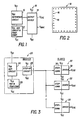
- a typical system for providing a reference voltage level is shown in Figure 1.
- a V bb reference circuit 10 is coupled to a fixed supply voltage, V cc .
- a temperature compensation and V cse reference circuit 12 is also coupled to this V bb reference circuit.
- An output driver circuit 14 provides a step down function to the desired voltage level, V cse and V bb1e , as a voltage reference where needed.
- Elements 10, 12 and 14 form a intermediate voltage reference circuit 16.
- a plurality of voltage reference circuits 16 are arranged around the edges of a semiconductor chip 18 as shown in Figure 2. Each of these circuits 16 reproduces the reference voltage level for supplying reference levels to designated I/0 (Input/Output) circuits.
- the present invention provides a circuit for providing a voltage reference level using a master circuit and a plurality of slave circuits.
- the master circuit includes a V bb reference circuit, a temperature compensation and V cse reference circuit, and a voltage step-up and buffering circuit.
- Each of the slave circuits has a pair of transistors in an emitter-follower configuration to step down the voltage and drive the circuitry requiring the voltage reference.
- the amount of circuitry and power dissipation required to generate each voltage reference level is reduced. This is done by providing the V bb reference circuit, V cs reference circuit and temperature compensation only once in the master circuit, with the output circuit only needing the driver.
- the master is provided with a step-up and buffer circuit and the slaves are provided with a step-down circuit as part of the driver. Because the slave uses an emitter-follower configuration to provide the necessary current, the extra transistor voltage drop must be compensated for with the step-up transistor configuration of the master circuit.
- the master circuit of the present invention can either be provided on a chip or externally from the chip, with each chip having a large number of slave circuits arranged around its edges. Thus, the circuitry required on a particular semiconductor chip is much reduced from that of the prior art.
- FIG. 3 is a block diagram of the present invention showing a master circuit 20 and a plurality of slave circuits 22.
- the master circuit includes a V bb reference circuit 24, a V cs reference circuit and temperature compensation circuit 26 and a step-up and buffer circuit 28.
- Each of the slave circuits has a step-down transistor 30 and a driver transistor 32.
- the step-down transistor also acts as a driver in an emitter-follower configuration with driver 32.
- Figure 4 shows the arrangement of the circuit of the present invention on a semiconductor chip 34.
- a pair of master circuits 20 are shown on two sides of the chip, with a large number of slave circuits 22 arranged around the edges.
- the slave circuits take up much less room than the prior art circuit which included all of the elements in one circuit.
- one master circuit may be used for 90 slave circuits, with each slave circuit driving 35 logic cells.
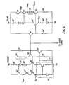
- FIG. 5 shows one embodiment of the present invention in which the master circuit may be located internally to the chip which contains the slave circuits.
- a V bb reference circuit is provided through resistor 36, diode 38 and resistor 40.
- the current from this V bb reference circuit is provided to a transistor 42 which has its emitter coupled to a temperature compensation circuit 26.
- the base of transistor 42 is also coupled to transistors 44 and 46 which provide a V cse voltage reference at their emitters.
- a pair of transistors 48 and 50 provide level shifting to V bb1e and V bb2e , respectively.
- the current through resistor 36, diode 38 and resistor 40 essentially sets up the V bb1e and V bb2e levels and is generated from the V cs reference circuit.
- the present invention shifts up the voltage by one diode level by the addition of a transistor 52.
- Transistor 52 is coupled to V cc through resistor 54 and to V ee through a resistor 56, which provides a level shifting function.
- the base of transistor 52 is coupled to the base of a transistor 58 in each slave circuit.
- Each transistor 58 provides a beta drop down to the level of transistor 42 at the base of a output transistor 60.
- resistors 62 and 64 are coupled to transistor 58 to provide a match to resistors 54 and 56 of transistor 52 to provide the same current density and cancel temperature effects.
- Transistor 52 not only steps up the voltage by one diode level, but also buffers out the temperature and beta effects of transistors 42, 44 and 46.
- Transistor 58 not only steps the voltage back down, but provides the current needed by output transistor 60, thus reducing the current needed to be produced from the master circuit to the base of transistor 58.
- a resistor 66 coupled to output transistor 60 is provided to prevent collector-emitter breakdown.
- a resistor 68 and a diode 70 are coupled between the emitter of transistor 60 and V ee .
- the base of transistor 52 is coupled to the collector of transistor 72 and level shifts the collector to a voltage two V be ( ⁇ ) above V cse .
- Transistors 58 and 60 in each slave circuit shift the voltage down two ⁇ to recreate voltage V cse .
- Transistors 51 and 46 and resistors 47 and 49 provide extra drive capability, and could be eliminated where not needed, as shown in Figure 6.
- Figure 6 shows an alternate embodiment of the present invention intended for use where the master circuit is on the same semiconductor chip as the slave circuits.
- the elements shown with a prime symbol i.e., 54′
- the primary difference is the addition of a third leg to the slave circuit having transistors 74, 76 and 78 along with optional diode 80 and resistor 82.
- This circuit allows the slave circuit to produce two or three higher voltage reference level signals.
- An extra resistor 73 has been added in the master circuit to adjust the temperature compensation from the 100K bias driver shown in Figure 5 to a 10K bias driver shown in Figure 6.
Landscapes
- Engineering & Computer Science (AREA)
- Physics & Mathematics (AREA)
- Microelectronics & Electronic Packaging (AREA)
- Logic Circuits (AREA)
- Radar, Positioning & Navigation (AREA)
- General Physics & Mathematics (AREA)
- Electromagnetism (AREA)
- Automation & Control Theory (AREA)
- Power Engineering (AREA)
- Computer Hardware Design (AREA)
- Computing Systems (AREA)
- General Engineering & Computer Science (AREA)
- Mathematical Physics (AREA)
- Nonlinear Science (AREA)
Applications Claiming Priority (2)
| Application Number | Priority Date | Filing Date | Title |
|---|---|---|---|
| US18101488A | 1988-04-13 | 1988-04-13 | |
| US181014 | 1988-04-13 |
Publications (2)
| Publication Number | Publication Date |
|---|---|
| EP0337314A1 true EP0337314A1 (de) | 1989-10-18 |
| EP0337314B1 EP0337314B1 (de) | 1994-01-12 |
Family
ID=22662526
Family Applications (1)
| Application Number | Title | Priority Date | Filing Date |
|---|---|---|---|
| EP19890106159 Expired - Lifetime EP0337314B1 (de) | 1988-04-13 | 1989-04-07 | Master-Slave-Pufferschaltung |
Country Status (4)
| Country | Link |
|---|---|
| EP (1) | EP0337314B1 (de) |
| JP (1) | JPH01311618A (de) |
| CA (1) | CA1301262C (de) |
| DE (1) | DE68912176T2 (de) |
Cited By (1)
| Publication number | Priority date | Publication date | Assignee | Title |
|---|---|---|---|---|
| EP0438655A3 (en) * | 1989-11-28 | 1991-10-16 | National Semiconductor Corporation | Ecl circuit for resistance and temperature bus drop compensation |
Citations (5)
| Publication number | Priority date | Publication date | Assignee | Title |
|---|---|---|---|---|
| WO1983000397A1 (en) * | 1981-07-20 | 1983-02-03 | Advanced Micro Devices Inc | A current source circuit |
| US4459540A (en) * | 1981-02-25 | 1984-07-10 | Mitsubishi Denki Kabushiki Kaisha | Constant voltage generating circuit |
| EP0140744A2 (de) * | 1983-09-21 | 1985-05-08 | Fujitsu Limited | Integrierte Schaltung |
| US4644249A (en) * | 1985-07-25 | 1987-02-17 | Quadic Systems, Inc. | Compensated bias generator voltage source for ECL circuits |
| EP0219937A2 (de) * | 1985-09-19 | 1987-04-29 | Advanced Micro Devices, Inc. | Gesteuerter ECL-Referenzgenerator |
-
1989
- 1989-04-07 DE DE1989612176 patent/DE68912176T2/de not_active Expired - Fee Related
- 1989-04-07 EP EP19890106159 patent/EP0337314B1/de not_active Expired - Lifetime
- 1989-04-12 CA CA000596422A patent/CA1301262C/en not_active Expired - Fee Related
- 1989-04-13 JP JP1092030A patent/JPH01311618A/ja active Pending
Patent Citations (5)
| Publication number | Priority date | Publication date | Assignee | Title |
|---|---|---|---|---|
| US4459540A (en) * | 1981-02-25 | 1984-07-10 | Mitsubishi Denki Kabushiki Kaisha | Constant voltage generating circuit |
| WO1983000397A1 (en) * | 1981-07-20 | 1983-02-03 | Advanced Micro Devices Inc | A current source circuit |
| EP0140744A2 (de) * | 1983-09-21 | 1985-05-08 | Fujitsu Limited | Integrierte Schaltung |
| US4644249A (en) * | 1985-07-25 | 1987-02-17 | Quadic Systems, Inc. | Compensated bias generator voltage source for ECL circuits |
| EP0219937A2 (de) * | 1985-09-19 | 1987-04-29 | Advanced Micro Devices, Inc. | Gesteuerter ECL-Referenzgenerator |
Cited By (1)
| Publication number | Priority date | Publication date | Assignee | Title |
|---|---|---|---|---|
| EP0438655A3 (en) * | 1989-11-28 | 1991-10-16 | National Semiconductor Corporation | Ecl circuit for resistance and temperature bus drop compensation |
Also Published As
| Publication number | Publication date |
|---|---|
| CA1301262C (en) | 1992-05-19 |
| DE68912176T2 (de) | 1994-07-07 |
| EP0337314B1 (de) | 1994-01-12 |
| DE68912176D1 (de) | 1994-02-24 |
| JPH01311618A (ja) | 1989-12-15 |
Similar Documents
| Publication | Publication Date | Title |
|---|---|---|
| US4628216A (en) | Merging of logic function circuits to ECL latch or flip-flop circuit | |
| US4644194A (en) | ECL to TTL voltage level translator | |
| CA1277722C (en) | Logic circuit | |
| EP0209464B1 (de) | Flip-Flop-Schaltung vom Master-Slave-Typ | |
| GB2076245A (en) | Emitter-coupled logic circuits | |
| US4931665A (en) | Master slave voltage reference circuit | |
| US5250860A (en) | Three-level cascode differential current switch | |
| EP0131205B1 (de) | Stromquellensteuerungspotentialgenerator für ECL-Logikschaltkreise | |
| US4409498A (en) | Transient controlled current switch | |
| EP0337314A1 (de) | Master-Slave-Pufferschaltung | |
| US4749885A (en) | Nonsaturating bipolar logic gate having a low number of components and low power dissipation | |
| JPH0345545B2 (de) | ||
| EP0447912A2 (de) | Schaltung mit einem Pegelkonverter für logische Signale | |
| US5029280A (en) | ECL circuit for resistance and temperature bus drop compensation | |
| JPS6331214A (ja) | 可変遅延回路 | |
| US4277698A (en) | Delay type flip-flop | |
| SU1531208A1 (ru) | Преобразователь уровн | |
| US5274285A (en) | Enhanced differential current switch compensating upshift circuit | |
| JP2776201B2 (ja) | フリップフロップ回路 | |
| JPH04249423A (ja) | マスタースライス型ecl回路 | |
| JP2846372B2 (ja) | 半導体回路 | |
| JPH0433410A (ja) | 半導体集積回路装置 | |
| JPH0389625A (ja) | 半導体論理回路 | |
| JP2681937B2 (ja) | フリツプフロツプ | |
| JPH0314231B2 (de) |
Legal Events
| Date | Code | Title | Description |
|---|---|---|---|
| PUAI | Public reference made under article 153(3) epc to a published international application that has entered the european phase |
Free format text: ORIGINAL CODE: 0009012 |
|
| AK | Designated contracting states |
Kind code of ref document: A1 Designated state(s): DE FR GB IT NL |
|
| 17P | Request for examination filed |
Effective date: 19900302 |
|
| 17Q | First examination report despatched |
Effective date: 19920819 |
|
| GRAA | (expected) grant |
Free format text: ORIGINAL CODE: 0009210 |
|
| AK | Designated contracting states |
Kind code of ref document: B1 Designated state(s): DE FR GB IT NL |
|
| REF | Corresponds to: |
Ref document number: 68912176 Country of ref document: DE Date of ref document: 19940224 |
|
| ET | Fr: translation filed | ||
| ITF | It: translation for a ep patent filed | ||
| PGFP | Annual fee paid to national office [announced via postgrant information from national office to epo] |
Ref country code: NL Payment date: 19940430 Year of fee payment: 6 |
|
| PGFP | Annual fee paid to national office [announced via postgrant information from national office to epo] |
Ref country code: FR Payment date: 19940823 Year of fee payment: 6 |
|
| PGFP | Annual fee paid to national office [announced via postgrant information from national office to epo] |
Ref country code: GB Payment date: 19940905 Year of fee payment: 6 |
|
| PLBE | No opposition filed within time limit |
Free format text: ORIGINAL CODE: 0009261 |
|
| STAA | Information on the status of an ep patent application or granted ep patent |
Free format text: STATUS: NO OPPOSITION FILED WITHIN TIME LIMIT |
|
| 26N | No opposition filed | ||
| PG25 | Lapsed in a contracting state [announced via postgrant information from national office to epo] |
Ref country code: GB Effective date: 19950407 |
|
| PG25 | Lapsed in a contracting state [announced via postgrant information from national office to epo] |
Ref country code: NL Effective date: 19951101 |
|
| GBPC | Gb: european patent ceased through non-payment of renewal fee |
Effective date: 19950407 |
|
| PG25 | Lapsed in a contracting state [announced via postgrant information from national office to epo] |
Ref country code: FR Effective date: 19951229 |
|
| NLV4 | Nl: lapsed or anulled due to non-payment of the annual fee |
Effective date: 19951101 |
|
| REG | Reference to a national code |
Ref country code: FR Ref legal event code: ST |
|
| PGFP | Annual fee paid to national office [announced via postgrant information from national office to epo] |
Ref country code: DE Payment date: 20010402 Year of fee payment: 13 |
|
| PG25 | Lapsed in a contracting state [announced via postgrant information from national office to epo] |
Ref country code: DE Free format text: LAPSE BECAUSE OF NON-PAYMENT OF DUE FEES Effective date: 20021101 |
|
| PG25 | Lapsed in a contracting state [announced via postgrant information from national office to epo] |
Ref country code: IT Free format text: LAPSE BECAUSE OF NON-PAYMENT OF DUE FEES;WARNING: LAPSES OF ITALIAN PATENTS WITH EFFECTIVE DATE BEFORE 2007 MAY HAVE OCCURRED AT ANY TIME BEFORE 2007. THE CORRECT EFFECTIVE DATE MAY BE DIFFERENT FROM THE ONE RECORDED. Effective date: 20050407 |