EP0335486B1 - Optische Informationsaufzeichnungsmethode - Google Patents
Optische Informationsaufzeichnungsmethode Download PDFInfo
- Publication number
- EP0335486B1 EP0335486B1 EP19890301389 EP89301389A EP0335486B1 EP 0335486 B1 EP0335486 B1 EP 0335486B1 EP 19890301389 EP19890301389 EP 19890301389 EP 89301389 A EP89301389 A EP 89301389A EP 0335486 B1 EP0335486 B1 EP 0335486B1
- Authority
- EP
- European Patent Office
- Prior art keywords
- recording
- pulse
- auxiliary
- light pulses
- light
- Prior art date
- Legal status (The legal status is an assumption and is not a legal conclusion. Google has not performed a legal analysis and makes no representation as to the accuracy of the status listed.)
- Expired - Lifetime
Links
Images


Classifications
-
- G—PHYSICS
- G11—INFORMATION STORAGE
- G11B—INFORMATION STORAGE BASED ON RELATIVE MOVEMENT BETWEEN RECORD CARRIER AND TRANSDUCER
- G11B7/00—Recording or reproducing by optical means, e.g. recording using a thermal beam of optical radiation by modifying optical properties or the physical structure, reproducing using an optical beam at lower power by sensing optical properties; Record carriers therefor
- G11B7/12—Heads, e.g. forming of the optical beam spot or modulation of the optical beam
- G11B7/125—Optical beam sources therefor, e.g. laser control circuitry specially adapted for optical storage devices; Modulators, e.g. means for controlling the size or intensity of optical spots or optical traces
- G11B7/126—Circuits, methods or arrangements for laser control or stabilisation
-
- G—PHYSICS
- G11—INFORMATION STORAGE
- G11B—INFORMATION STORAGE BASED ON RELATIVE MOVEMENT BETWEEN RECORD CARRIER AND TRANSDUCER
- G11B7/00—Recording or reproducing by optical means, e.g. recording using a thermal beam of optical radiation by modifying optical properties or the physical structure, reproducing using an optical beam at lower power by sensing optical properties; Record carriers therefor
- G11B7/002—Recording, reproducing or erasing systems characterised by the shape or form of the carrier
- G11B7/0037—Recording, reproducing or erasing systems characterised by the shape or form of the carrier with discs
-
- G—PHYSICS
- G11—INFORMATION STORAGE
- G11B—INFORMATION STORAGE BASED ON RELATIVE MOVEMENT BETWEEN RECORD CARRIER AND TRANSDUCER
- G11B7/00—Recording or reproducing by optical means, e.g. recording using a thermal beam of optical radiation by modifying optical properties or the physical structure, reproducing using an optical beam at lower power by sensing optical properties; Record carriers therefor
- G11B7/004—Recording, reproducing or erasing methods; Read, write or erase circuits therefor
- G11B7/0045—Recording
-
- G—PHYSICS
- G11—INFORMATION STORAGE
- G11B—INFORMATION STORAGE BASED ON RELATIVE MOVEMENT BETWEEN RECORD CARRIER AND TRANSDUCER
- G11B7/00—Recording or reproducing by optical means, e.g. recording using a thermal beam of optical radiation by modifying optical properties or the physical structure, reproducing using an optical beam at lower power by sensing optical properties; Record carriers therefor
- G11B7/004—Recording, reproducing or erasing methods; Read, write or erase circuits therefor
- G11B7/006—Overwriting
Definitions
- This invention relates to a method of recording an information signal on an optical information recording medium by irradiating high density energy flux thereon.
- a phase difference type optical disk is one method available in which the state change either between an amorphous state and a crystal state or between two different crystal states is used.
- Thin recording film to be used in this method features that either an amorphous state or a crystal state is formed in accordance with temperature rising and cooling conditions when a laser beam is irradiated and that these states are changeable reversibly.
- the amorphous state and the crystal state are different from each other in the complex ideas of refraction, which can be expressed by refractive index n and extinction coefficient k, and the signal recording is achieved using thus generated difference in transmittance and reflectance of a recording medium.
- refractive index n and extinction coefficient k refractive index
- k refractive index
- EP-A-0265971 and EP-A-0218243 also describe phase-change type erasable optical disks.
- the laser power is modulated to have three energy levels, a recording (high) power level, an erasing (medium) power level and a cooling (low) power level.
- the light intensity of the erasing light beam is gradually decreased and turned off.
- a first object of this invention is to provide a method of realizing a high erasability when a signal is to be overwritten on a recording medium using a single laser beam.
- a second object of this invention is to provide a recording method which makes it possible to provide a reproduced signal with less waveform distortion.
- the present invention provides a method of recording an information signal by using a single light beam on a recording medium which is reversibly changeable between first and second states which are optically distinguishable from each other, said method having a step of applying the light beam, as a recording light pulse, in response to the information signal to the recording medium for a predetermined duration to cause the recording medium to melt and become the first state thereby forming a record mark, characterized by modifying the light beam before and after the recording light pulse into a train of auxiliary light pulses each having a shorter duration than the predetermined duration and applying the train of auxiliary pulses to an area of the recording medium before and after the record mark to cause the area to melt and become a state substantially identical to the second state.
- the light beam applied to the area between the record marks may preferably consist of a train of auxiliary light pulses each having a pulse width smaller enough than the predetermined duration of the writing laser beam.
- the modification of the light beam may be such that the peak power level is reduced. It is the only requirement for the light beam applied to the area between the record marks to have an energy which does not cause the recording medium to change its state to the first state.
- the present invention provides a method of recording an information signal by using a single light beam on a recording medium which is reversibly changeable between two states which are optically distinguishable from each other, said method having a step of applying the light beam, as a recording light pulse, in response to the information signal to the recording medium for a predetermined duration to cause the recording medium to melt and cause a state change from one of the two states to the other thereby forming a record mark, characterized by modulating the recording light pulse into a plurality of light pulses so as to have a higher energy at the beginning of the predetermined duration than an energy at the ending of the predetermined duration thereby causing the recording medium to melt uniformly at an area applied with the recording light pulse and cause the state change from one of the two states to the other to form said area into a record mark having substantially a symmetrical shape.
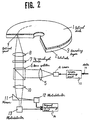
- Fig. 2 shows an optical disk and an optical recording system in accordance with one embodiment of this invention.
- Optical disc 1 is fundamentally made of a substrate 2 and a recording layer 3 disposed on the substrate 2.
- the substrate 2 either resins such as, for example, polymethylmethacrylate (PMMA) and polycarbonate (PC), or glass can be used.
- PMMA polymethylmethacrylate
- PC polycarbonate
- GeTe GeTe, GeSb2Te4, Ge2Sb2Te5, InSe system, InSeTlCo system, GeSnTeAn system, SeSbTeSe system, SeSnTeO system, SeTeS system or the like can be used in case that the phase change is to be taken place between an amorphous state and a crystal state, and InSb system, AgZn system or the like can be used in case that the phase change is to be taken place between two crystal states.
- Recording on the recording layer 3 is generally carried out by using, as a laser beam source, a semiconductor laser 4 with a wavelength of 780 nm.
- Light beam from the semiconductor laser 4 is made parallel by a collimator lens 5, reflected by a polarizing beam splitter 6, passed through a quarter wave length plate 7, and finally focused by an objective lens 8 to form a circular spot 9 of approximately 1 »m in diameter, which is a limit on wave length, on the recording layer 3 of the optical disk 1.
- the light beam reflected by the recording layer 3 passes again through the objective lens 8, the quarter wave length plate 7, the polarizing beam splitter 6 and a lens 10 in this order.
- a part of the light beam thus reflected and passed therethrough is reflected by a mirror 11 to condense onto a photodetector 12 thereby being used for focus control in a signal reproducing circuit 14.
- the rest of the light beam is received by a photodetector 13 thereby to be used for tracking control and signal reproduction in the signal reproducing circuit 14.
- the writing is carried out by modulating the power of the semiconductor laser 4 using a laser driving circuit 15 according to a data 16.
- Figs. 3 (a) and (c) each shows the change of the output power level of a laser beam, in which, (a) is for the first time recording and (c) for the second time recording.
- the output power level thereof changes between a writing power Pw and an erasing power Pe according to the input signal.
- Observation results of recorded areas are illustrated in Fig. 3 (b) and (d) corresponding to the beam irradiation as patterned in Figs. (a) and (c), respectively. Also, for the reason that no examination was given upon the shape of a recording mark, the mark is approximated to be symmetrical in shape.
- an amorphous mark 17 was formed where the writing power Pw was irradiated, and a large crystal grain 18 was observed surrounding the amorphous mark 17. Also, where the erasing power Pe was irradiated, a small crystal grain (microcrystal) 19 was observed.
- microcrystal which is precipitately crystalized from the solid phase state is defined as “solid-phase crystal”
- crystal which is formed in the cooling process from the melt state is defined as “melt-phase crystal”.
- the recording method of an optical information according to this invention restricts the effect of the melt-phase crystal formed surrounding the recording mark as shown above. That is, in order to improve the erasability, an effective modulation is applied to the output waveform of a laser beam to be irradiated onto the optical disk 1.
- the modulation and its effect will be explained below by referring to Fig. 1.
- the waveform of a signal to be recorded on an optical disk is shown in Fig. 1 (a), and the waveform of an output beam from a semiconductor laser modulated in strength by the method of this invention is shown in Fig. 1 (b).
- Fig. 1 (c) shows the temperature change of the recording layer generated when the beam was irradiated.
- Fig. 1 (d) shows the transmission-type electron microscopic observations of the shape of the recorded mark formed actually on the recording layer.
- the output waveform (b) of the semiconductor laser is composed of writing pulses (P1 and P2) which correspond to the level "1" of the code signal (a) and auxiliary pulses (S1 and S2) which occur between the writing pulses.
- Pulse width Ws of each auxiliary pulse is made such as to be smaller than the shortest pulse width of pulse widths Ww of the writing pulse.
- the temperature where irradiation was made is varied as shown in Fig. 1 (c). Namely, an area where the writing pulses P1 and P2 were irradiated is heated to a temperature exceeding the melting point Tm of a material of the recording layer, so that amorphous marks 17 each having a melt-phase crystal surrounding thereto are formed corresponding to the input signal.
- Fig. 4 shows a laser driving circuit for the recording method of this invention.
- This circuit comprises four kinds o current sources according to the modulation power level of the laser beam.
- Current sources 23, 24, 25 and 26 correspond to the reading power, peak power of the writing pulse, peak power of the auxiliary pulse and the erasing power, respectively.
- Each power level can be set to a desired value by varying the current of a corresponding current source.
- Each current source becomes a laser driving output through respective switching circuits 27, 28, 29 and 30.
- the writing gate signal 22 is turned “ON”, and the switching circuit 27 is turned “OFF”, so that no flow of a reading current results.
- the switching circuit 30 is turned “ON”, and a current corresponding to the erasing power Pe is outputted.
- a data 16 is coded by an encoder 33 output a code signal 34.
- This coding can be made in any modulation form, for example, FM code, MFM code, 2-7 code, 8-14 code or the like is general.
- a clock signal 35 is simultaneously outputted together with the code signal 34.
- These signals thus outputted are passed through a writing pulse gate 36 and an auxiliary pulse gate 37 thereby to be outputted as a writing pulse gate signal 36 S and as an auxiliary pulse gate signal 37 S, respectively.
- These signals 36 S and 37 S are to switch the current source 24 for the writing pulse and the current source 25 for the auxiliary pulse, respectively.
- Combined current of the current source 24, 25 and 26 is outputted as the laser driving output 32.
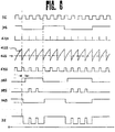
- a concrete example showing the writing pulse gage 36 and auxiliary pulse gate 37 is shown in Fig. 5 and their timing charts are shown in Fig. 6.
- the code signal 34 generated by the encoder 33 and a clock signal generated in the encoding process, particularly the clock signal 35 of higher order are used.
- the clock signal 35 becomes a leading edge signal 40 S of the clock by a delay element 38, an inverter 39 and an AND gate 40.
- Capacitor 42 is charged by a current which is supplied from a power source "+V" and passed through a resistor 43, and discharged by driving a switching circuit 41 by the clock signal 40 S, thus a signal 42 S being outputted.
- Comparator 44 compares a potential signal 46 S obtained by dividing a potential "+V" into a ratio of resistors 45 and 46 with the signal 42S thus outputted thereby to produce a signal 44 S.
- the signal 44 S is outputted to an AND gate 47.
- the code signal 34 becomes a signal 50 S for determining the time period during which the auxiliary pulse is generated by a delay element 48, an OR circuit 49 and an inverter 50 to be inputted to the AND gate 47.
- the auxiliary pulse gate signal 37S is outputted from the AND gate 47.
- the code signal 34 becomes the writing gate pulse signal 36 S through a delay element 51.
- the switching circuits 28, 29 and 30 are operated by the writing gate signal 22, writing pulse gate signal 36 S and auxiliary pulse gate signal 37 S, respectively, to produce the laser driving signal 32.
- An optical disk 1 which comprises a substrate 2 of polycarbonate and a recording layer 3 of Ge2Sb2Te5 which has thermal diffusion layers of Zn S disposed on both sides thereof, was rotated at a linear velocity of 15 m/s thereby to carry out a writing.
- Writing and erasing characteristics were analyzed in such a way that, using two frequencies, 2.5 MHz and 2.14 MHz, a signal of 2.5 MHz was recorded first and C/N (carrier - to - noise ratio) value was measured, and then, a signal of 2.14 MHz was written and the C (carrier) component of the 2.5 MHz signal which had been written in advance was measured. The difference of the C component thus measured from the initial value was defined as erasability.
- Pulse width Ww of each of the writing pulses P1 and P2 for forming recording marks was 200 nS, and the periods T1 and T2 between the writing pulses P1 and P2 were 400 nS and 467 nS from the above-mentioned condition, respectively.
- the power of each pulse was such that the writing power level Pw was 16 mW, erasing power level Pe was 6 mW, and the peak power of the auxiliary pulse was identical to that of the writing power level.
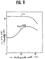
- the pulse width Ws of the auxiliary pulse can be set arbitrarily by changing either the capacity of the capacitor 42 or the value of the resistor 43 in Fig. 5.
- the pulse width Ws of the supplementary pulse is 0 nS corresponds to the erasing according to the prior art, in which erasability is smaller such as to be 23 dB.
- the pulse width Ws is increased, the erasability is improved, particularly in the range of 20 to 40 nS, it exceeds 35 dB. This is considered due to the fact that the area where the auxiliary pulse was irradiated was melted once and then crystallized.
- Modulated waveform of the laser beam was identical to that shown in Fig. 3 (a) and the frequency thereof was varied according to the pitch of the recorded marks. Also, the duty factor of the writing pulse was 50% (the pulse width and pulse interval are equal to each other). In case that the mark pitch exceeds 3 »m, the C/N remains constant, but in case that it becomes below 2 »m, the C/N is decreased gradually, for example, when it is 1 »m, the C/N value decreases 20 dB.
- the wave length of a laser beam was 0.78 »m
- the ratio of the mark pitch and the wave length of the reading beam was about 1.2 times, and it was revealed that if the value of this ratio is either 1.2 or less, its effect on the read signal can be reflected.
- the spot diameter obtained when a laser beam is condensed up to the resolution limit can be supposed to be proportional to the wave length of the laser beam.
- the peak power level of the auxiliary pulse is identical to the writing power level Pw. But, when the peak power level is made higher than the Pw, the pulse width may be made smaller to effect the erasability improvement. Inversely, when the peak power level is made smaller than the Pw, the pulse width to be required is widened, but when made further smaller, the recording material can not be heated to the melting point even if the pulse width to be required is widened, which means that the effects of this invention can not be obtained.
- the peak power level of the auxiliary pulse identical to the writing power level Pw is advantageous because the power level of the laser beam may be only two. Namely, a single current source can be used in common for producing the writing pulse and auxiliary pulse, pulse of the current source 25 can be used in common.
- EXAMPLE 1 modulation of the erasing power was described, but in this EXAMPLE 2, description will be made on a method of further reducing the waveform distortion of a reproduced signal by adding modulation to the writing power.
- Waveform distortion is mainly caused by asymmetry of a recorded mark.
- the phenomenon that the recorded mark becomes asymmetrical is a peculiar one in the heat mode recording. That is, a phase change type recording medium and a optomagnetic recording medium for which the magnetic Kerr effect of a thin ferroelectric film is applied are all such that an absorbed beam is once converted into a heat and a record mark is taken place by the heat thus converted.
- a phase change type recording medium and a optomagnetic recording medium for which the magnetic Kerr effect of a thin ferroelectric film is applied are all such that an absorbed beam is once converted into a heat and a record mark is taken place by the heat thus converted.
- the balance between the heat generation and its diffusion differs due to irradiation time of a beam (pulse width), power or the like, the shape of the recorded mark will be distorted.
- Recording medium 52 was structured so as to be generally used in a rewritable type optical disk.
- GeTe thin film of 90 nm thick whose upper and lower surfaces respectively have ZnS thin films of 100 and 200 nm thick in a sandwich manner was formed on a polycarbonate substrate with a thickness of 2 mm.
- the same substrate as the above-mentioned one was affixed thereon using an adhesive.
- the disk thus formed was turned at a linear velocity of 22.5 m/s.
- Pulse beam 54 (in case there exists no erasing power) or pulse beam 55 (in case there exists the erasing power) was irradiated onto a track 53.
- the writing power to be used was 10 mW.
- the pulse width to be irradiated was 88.8 nS.
- the recording medium moved a small distance of 2 »m during irradiation of the pulse beam.
- Fig. 10 (b) shows the calculated result of the temperature change on the center line of the track at each of the beginning point, intermediate point and finishing point of each mark writing.
- the recording mark had a shape extended irradiation-wise. If the writing power is decreased in order to solve this problem, the temperature at the central portion will be decreased, so that it is anticipated that the mark width can be reduced.
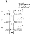
- Fig. 11 shows the observations using a transmission electron microscope on the shape of a mark 57 written on a guide track 56 of the optical disk. In this case, to emphasize the shape of the record mark, the boundary between the melt-phase crystal and the solid-phase crystal was omitted.
- Figs 11 (a), (b) and (c) are the case that the erasing power does not exist, the case that has the same power as the writing power of (a) and yet the erasing power exists, and the case that has the same power as the erasing power of (b) and the writing power is decreased, respectively.
- Point 57 indicates the point where the laser beam is changed from an erasing power 60 to a writing power 59, and a point 58 does the point where to be changed from the writing power to the erasing power.
- the record mark having a shape extended irradiation-wise was formed.
- the writing power was lowered, the record mark having a narrow width as a whole was obtained.
- such a trend that the width of a mark is narrow at the beginning point of writing and wide at the finishing point thereof could be recognized. From the results shown above, it can be said that it is extremely difficult to demodulate a signal written by using a read signal obtained from such a mark as has an error in length and a distortion in shape with no error.
- This invention is to solve the above-mentioned problems by subjecting a density change of high frequency further to an optical energy to be modulated according to an information signal.
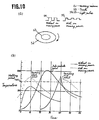
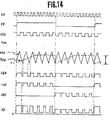
- Fig. 12 an example showing a modified waveform of a beam to be irradiated and its features will be shown below in detail.
- Fig. 13 shows an example of a circuit structure
- Fig. 14 is its timing chart.
- the circuit structure is resemble to that shown in Fig. 5, and pulses having different pulse widths are generated using the difference in charging and discharging characteristic of two capacitors 67 and 73.
- Clock signal 35 of high order drives a switching circuit 64 through a flip-flop 63.
- Capacitor 66 is charged by a current passed through a resistor 67 from a power source "+V" and discharged through a discharging resistor 65 when the switching circuit 64 was driven. At this time, a potential signal 66S is inputted into a comparator 68.
- code signal 34 is similarly passed through a delay element 69 and an exclusive OR gate 70 to output an edge current 73 3 of the coded signal thereby to drive a switching circuit 71.
- Capacitor 72 is charged through a resistor 73 having a suitably high resistance as compared with the resistor 67 and a potential 72 S is increased up to the rated voltage of a Zener diode 74, thereafter indicating a constant value.
- the potential signal 72 S of this capacitor 72 is inputted to the comparator 68. From the comparator 68, a signal obtained by comparing the signals thus inputted, 66 S and 72 S, is outputted for inputting to AND gates 75 and 76.
- the code signal 34 is inputted to the AND gate 75 or the AND gate 76 through an inverter 77 thereby to output a writing pulse gate signal 36 S and a supplementary gate signal 37 S, respectively.
- the length of a record mark can be accurately determined as shown below. Namely, the rise position and fall position during the writing become possible to be precisely determined.
- Fig. 15 shows the temperature change when an overwrite was carried out using the modulated waveform shown in Fig. 12.
- the structure of the optical disk is identical to that shown in Fig. 10, and the result shown is the temperature change at the finishing point of writing.
- the period T4 and the power level Pw were set such as to be 1/6 of T3 and two times of the Pe, respectively.
- the duty of pulse width was 90%, 80%, 70%, 60%, 60% and 60% in the order from a first pulse.
- the melting time was shortened as compared with the example shown in Fig. 10, so that it is supposed to be difficult to give an effect up to the rear portion of a recording mark.
- Fig. 16 shows the observation result of the record mark.
- the shape of a record mark thus obtained was symmetrical at the beginning point and finishing point of writing and its length was of a specified one. Temperature rise could be carried out more smoothly when T4 was at value not exceeding one half of T3.
- the method shown in EXAMPLE 2 in which the pulse width of a writing pulse is changed in order, is a useful method for use in optical recording media of not only the rewriting type but also the write-once type.
- an optical recording member of such a write-once type With an optical recording member of such a write-once type, an asymmetrical record mark in shape as shown in Fig. 11 (a) is formed.
- the area equivalent to this record mark may be, based on the recording material and the recording principle, considered to have various cases such as when the change is made from the amorphous state to the crystal state, when the shape of a recording material is evaporated, or the like.
- the same problem must be pointed out in that the record mark width at the beginning point of writing is narrow and that at the finishing point thereof is wide, so that a reproduced waveform will be distorted.
- the beam irradiating condition for forming one record mark is set so that the energy density can be made high at the beginning point of writing and gradually decreased as it moves toward the finishing point thereof.
- the modulated waveform in this case can be obtained by omitting parts relating the writing pulses of circuits shown in EXAMPLE 2, for example, the current sources 25 and 26.
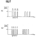
- Fig. 17 shows waveforms written on a medium of the write-once type.
- setting is made so that a plurality of pulses are prepared with respect to one piece of record mark and further a pulse width of these pulses becomes wide at the beginning point of writing and narrow at the finishing point thereof.
- an optical disk which was made of a polycarbonate substrate 2 and a Te-0-Pd system recording layer 3 was used and the writing was carried out under conditions such as to be rotated at a linear velocity of 3 m/S and irradiated at a frequency of 833 kHz for the comparison purpose of this invention with the prior art.
- Evaluation of the shape of a record mark was achieved by measuring the spectrum strength of a reproduced signal using a spectrum analyzer.
- SHD secondary harmonic distortion
- the optimum peak power was 4.5 mW and the SHD value was 25 dB.
- the modulated waveform as shown in Fig. 17 (a) was used under conditions such that the peak power was 8 mW, each pulse space was 300 nS and pulse widths of each pulse, Wa, Wb and Wc, were 180 nS, 150 nS and 140 nS, respectively, the SHD value was 38 dB, which means that the SHD value was increased by 13 dB as compared with the method of the prior art and the record mark is improved in symmetry. By increasing the number of pulses and selecting their pulse width, the SHD value can be further improved.
- modulated waveform as shown in Fig. 17 (b) is available. Contrary to the case shown in Fig. 17 (a) in which the optical energy is concentrated upon the beginning point of writing of a record mark by changing the pulse width of each pulse, in Fig. 12 (b) the pulse width of one pulse and the peak power are held constant and the pulse interval is subjected to modulation. Namely, by setting the pulse interval Da at the beginning point of writing so as to be smaller than successive pulse intervals Db and Dc, the optical energy is concentrated upon the head portion of a record mark.
- writing was carried out in the same manner as above.
- the writing conditions were such that the peak power was 8 mW, the pulse width was 120 nS and pulse spaces Da, Db and Dc were 150 nS, 200 nS and 250 nS, respectively.
- the SHD value obtained was 36 dB, being effective to improve the symmetry of the recording mark.
- the method for concentrating the optical energy upon the beginning portion of a record mark such a method that the pulse interval and pulse width of a plurality of pulses are held constant and the pulse power at the beginning point of writing is set so as to be higher than that of successive pulses is available. In this case, symmetry of a recording mark can be improved.
Landscapes
- Physics & Mathematics (AREA)
- Optics & Photonics (AREA)
- Optical Recording Or Reproduction (AREA)
Claims (21)
- Verfahren zum Aufzeichnen eines Informationssignals unter Benutzung eines Einzellichtstrahls, an einem reversibel zwischen ersten und zweiten voneinander optisch unterscheidbaren Zuständen veränderbaren Aufzeichnungsmedium, welches Verfahren einen Schritt besitzt, daß der Lichtstrahl als ein Aufzeichnungs-Lichtimpuls in Abhängigkeit von dem Informationssignal während einer vorbestimmten Zeitlänge an das Aufzeichnungsmedium angelegt wird, um das Aufzeichnungsmedium aufschmelzen in den ersten Zustand kommen zu lassen und dadurch eine Aufzeichnungs-Markierung zu bilden,
dadurch gekennzeichnet, daß der Lichtstrahl vor und nach dem Aufzeichnungs-Lichtimpuls zu einer Folge von Hilfs-Lichtimpulsen mit jeweils einer kürzeren als der vorbestimmten Zeitlänge modifiziert und die Folge von Hilfsimpulsen auf einen Bereich des Aufzeichnungsmediums vor und nach der Aufzeichnungs-Markierung angelegt wird, um den Bereich schmelzen und in einen Zustand kommen zu lassen, der im wesentlichen identisch mit dem zweiten Zustand ist. - Verfahren nach Anspruch 1, bei dem der erste Zustand ein amorpher Zustand und der zweite Zustand ein kristalliner Zustand ist.
- Verfahren nach Anspruch 1, das im wesentlichen die folgende Bedingung erfüllt:

wobei Ts eine Zeitdauer der Hilfs-Lichtimpulse, L eine Wellenlänge des zum Lesen des auf dem Aufzeichnungsmedium aufgezeichneten Informationssignals benutzten Leselichtstrahls und V eine Relativ-Geschwindigkeit zwischen dem Aufzeichnungsmedium und dem Lese-Lichtstrahl ist. - Verfahren nach Anspruch 1, bei dem ein Spitzen-Leistungspegel jedes Hilfs-Lichtimpulses gleich einem Spitzen-Leistungspegel des Aufzeichnungs-Lichtimpulses ist.
- Verfahren nach Anspruch 1, bei dem der Aufzeichnungs-Lichtimpuls aus einer Folge einer Vielzahl von Hilfs-Aufzeichnungs-Lichtimpulsen besteht.
- Verfahren nach Anspruch 5, bei dem ein als erster auftretender Hilfs-Lichtimpuls die längste Zeitdauer und ein zuletzt auftretender Hilfs-Lichtimpuls die kürzeste Zeitdauer in der Folge der Hilfs-Lichtimpulse besitzt.
- Verfahren nach Anspruch 5, bei dem die Hilfs-Lichtimpulse Impuls-Zeitdauern besitzen, die in der Folge von Hilfs-Lichtimpulsen graduell verringert werden.
- Verfahren nach Anspruch 5, bei dem die Hilfs-Lichtimpulse Impuls-Zeitdauern besitzen, die graduell verringert werden, bis sie einen vorbestimmten konstanten Wert erreichen und danach den vorbestimmten konstanten Wert in der Folge der Hilfs-Lichtimpulse aufrechterhalten.
- Verfahren nach Anspruch 5, bei dem ein zuerst auftretender Hilfs-Aufzeichnungslichtimpuls die längste Zeitdauer und ein zuletzt auftretender Hilfs-Aufzeichnungslichtimpuls die kürzeste Zeitdauer in der Folge der Vielzahl von Hilfs-Aufzeichnungslichtimpulsen besitzt.
- Verfahren nach Anspruch 5, bei dem die Vielzahl von Hilfs-Aufzeichnungslichtimpulsen Impuls-Zeitdauern besitzt, die in der Folge der Vielzahl von Hilfs-Aufzeichnungslichtimpulsen graduell reduziert sind.
- Verfahren nach Anspruch 5, bei dem die Vielzahl von Hilfs-Aufzeichnungslichtimpulsen Impuls-Zeitdauern besitzt, die graduell reduziert werden, bis sie einen vorbestimmten konstanten Wert erreichen und danach der vorbestimmte konstante Wert in der Folge der Vielzahl von Hilfs-Aufzeichnungslichtimpulsen aufrecht erhalten wird.
- Verfahren nach Anspruch 5, bei dem die Folge von Hilfs-Lichtimpulsen die gleiche Frequenz wie und geringeren Spitzen-Leistungspegel besitzt als die Folge der Vielzahl von Hilfs-Aufzeichnungslichtimpulsen.
- Verfahren zum Aufzeichnen eines Informationssignals unter Benutzung eines Einzellichtstrahls auf einem reversibel zwischen zwei optisch voneinander unterscheidbaren Zuständen änderbaren Aufzeichnungsmedium, wobei das Verfahren einen Schritt besitzt, daß ein Lichtstrahl als ein Aufzeichnungs-Lichtimpuls in Abhängigkeit von einem Informationssignal während einer vorbestimmten Zeitdauer an das Aufzeichnungsmedium angelegt wird, um das Aufzeichnungsmedium schmelzen zu lassen und eine Zustandsänderung von einem der beiden Zustände zu dem anderen zu verursachen, die eine Aufzeichnungs-Markierung bildet,
dadurch gekennzeichnet, daß der Aufzeichnungs-Lichtimpuls zu einer Vielzahl von Lichtimpulsen moduliert wird, die an dem Beginn der vorbestimmten Zeitdauer eine höhere Energie besitzen, als die Energie am Ende der vorbestimmten Zeitdauer ist, und dadurch das Aufzeichnungsmedium gleichmäßig in einem mit den Aufzeichnungs-Lichtimpulsen beaufschlagten Bereich schmelzen lassen und die Zustandsänderung von einem der beiden Zustände in den anderen zu verursachen zur Ausbildung des Bereiches zu einer Aufzeichnungs-Markierung mit einer im wesentlichen symmetrischen Form. - Verfahren nach Anspruch 13, bei dem der Aufzeichnungs-Lichtimpuls aus einer Folge einer Vielzahl von Lichtimpulsen besteht, deren Impulsdauer sich allmählich von dem Beginn zum Ende der vorbestimmten Zeitdauer verringert.
- Verfahren nach Anspruch 14, das im wesentlichen die folgende Bedingung erfüllt:

wobei Ts eine Zeitdauer der Vielzahl von Lichtimpulsen, L eine Wellenlänge eines zum Lesen des auf dem Aufzeichnungsmedium aufgezeichneten Informationssignals benutzten Leselichtstrahls und V eine Relativ-Geschwindigkeit des Leselichtstrahls zu dem Aufzeichnungsmedium ist. - Verfahren nach Anspruch 14, bei dem Vielzahl von Lichtimpulsen eine gleiche Impuls-Zeitdauer besitzt.
- Verfahren nach Anspruch 14, bei dem die Vielzahl von Lichtimpulsen den gleichen Spitzen-Leistungspegel besitzt.
- Verfahren nach Anspruch 13, bei dem der Aufzeichnungs-Lichtimpuls aus einer Folge von einer Vielzahl von Lichtimpulsen besteht, deren Impulsdauern allmählich von dem Beginn zum Ende der vorbestimmten Zeitdauer anwachsen.
- Verfahren anch Anspruch 18, bei dem die Vielzahl von Lichtimpulsen die gleiche Impulsdauer besitzt.
- Verfahren nach Anspruch 18, bei dem die Vielzahl von Lichtimpulsen den gleichen Spitzen-Leistungspegel besitzt.
- Verfahren nach Anspruch 13, bei dem der Aufzeichnungs-Lichtimpuls aus einer Folge einer Vielzahl von Lichtimpulsen besteht, deren Spitzen-Leistungspegel graduell vom Beginn zum Ende der vorbestimmten Zeitdauer abnehmen.
Applications Claiming Priority (4)
| Application Number | Priority Date | Filing Date | Title |
|---|---|---|---|
| JP73610/88 | 1988-03-28 | ||
| JP63073610A JP2625843B2 (ja) | 1988-03-28 | 1988-03-28 | 光学情報記録方法 |
| JP63080839A JP2574379B2 (ja) | 1988-03-31 | 1988-03-31 | 光学的情報記録消去方法 |
| JP80839/88 | 1988-03-31 |
Publications (3)
| Publication Number | Publication Date |
|---|---|
| EP0335486A2 EP0335486A2 (de) | 1989-10-04 |
| EP0335486A3 EP0335486A3 (de) | 1991-10-23 |
| EP0335486B1 true EP0335486B1 (de) | 1994-06-15 |
Family
ID=26414751
Family Applications (1)
| Application Number | Title | Priority Date | Filing Date |
|---|---|---|---|
| EP19890301389 Expired - Lifetime EP0335486B1 (de) | 1988-03-28 | 1989-02-14 | Optische Informationsaufzeichnungsmethode |
Country Status (2)
| Country | Link |
|---|---|
| EP (1) | EP0335486B1 (de) |
| DE (1) | DE68916084T2 (de) |
Cited By (1)
| Publication number | Priority date | Publication date | Assignee | Title |
|---|---|---|---|---|
| CN1310218C (zh) * | 2001-09-29 | 2007-04-11 | 三星电子株式会社 | 用于在光记录介质上记录数据的方法 |
Families Citing this family (11)
| Publication number | Priority date | Publication date | Assignee | Title |
|---|---|---|---|---|
| EP0669612B1 (de) * | 1989-12-20 | 2000-03-08 | Sony Corporation | Optisches Aufzeichnungsgerät |
| US5513167A (en) * | 1989-12-20 | 1996-04-30 | Sony Corporation | Optical recording apparatus |
| JP3259204B2 (ja) * | 1992-10-21 | 2002-02-25 | 株式会社ニコン | 光記録方法及び光記録のパルストレイン条件決定方法 |
| EP0594425A3 (en) * | 1992-10-21 | 1996-10-09 | Nippon Kogaku Kk | Pulse train condition/heat shut off condition determination method and apparatus for optical recording, and optical recording method and apparatus |
| JPH06267123A (ja) * | 1992-10-28 | 1994-09-22 | Nikon Corp | 光磁気ディスクに熱遮断方式及びパルストレイン方式で オーバーライトする場合における記録条件決定方法、 同記録条件決定装置、光磁気記録方法及び光磁気記録 装置 |
| US5297129A (en) * | 1992-12-24 | 1994-03-22 | Optical Disc Corporation | Waveform shaping method and apparatus for optical recording |
| JPH08227543A (ja) * | 1995-02-21 | 1996-09-03 | Nikon Corp | 情報消去装置及び情報記録装置 |
| JPH0927154A (ja) * | 1995-07-10 | 1997-01-28 | Fujitsu Ltd | 光磁気ディスク装置 |
| US6028686A (en) * | 1997-03-04 | 2000-02-22 | Mirell; Stuart Gary | Energy-depleted radiation apparatus and method |
| EP0916132A2 (de) * | 1997-05-01 | 1999-05-19 | Koninklijke Philips Electronics N.V. | Verfahren und vorrichtung zum beschreiben optischer aufzeichnungsträger |
| US7525890B2 (en) | 2001-09-29 | 2009-04-28 | Samsung Electronics Co., Ltd. | Method of and apparatus for recording data on optical recording medium |
Family Cites Families (2)
| Publication number | Priority date | Publication date | Assignee | Title |
|---|---|---|---|---|
| KR910001328B1 (ko) * | 1985-10-08 | 1991-03-04 | 마쯔시다덴기산교 가부시기가이샤 | 정보기록재생장치 |
| US4939717A (en) * | 1986-10-31 | 1990-07-03 | Matsushita Electric Industrial Co., Ltd. | Method and apparatus for erasing and recording information using three power levels |
-
1989
- 1989-02-14 DE DE1989616084 patent/DE68916084T2/de not_active Expired - Lifetime
- 1989-02-14 EP EP19890301389 patent/EP0335486B1/de not_active Expired - Lifetime
Cited By (2)
| Publication number | Priority date | Publication date | Assignee | Title |
|---|---|---|---|---|
| CN1310218C (zh) * | 2001-09-29 | 2007-04-11 | 三星电子株式会社 | 用于在光记录介质上记录数据的方法 |
| CN100373466C (zh) * | 2001-09-29 | 2008-03-05 | 三星电子株式会社 | 用于在光记录介质上记录数据的装置 |
Also Published As
| Publication number | Publication date |
|---|---|
| EP0335486A2 (de) | 1989-10-04 |
| EP0335486A3 (de) | 1991-10-23 |
| DE68916084D1 (de) | 1994-07-21 |
| DE68916084T2 (de) | 1995-02-16 |
Similar Documents
| Publication | Publication Date | Title |
|---|---|---|
| US5291470A (en) | Optical information recording method | |
| EP0265971B1 (de) | Verfahren zur optischen Informationsaufzeichnung | |
| EP0405610B1 (de) | Optisches Informationsaufzeichnungsverfahren | |
| JP2797733B2 (ja) | 光学情報記録部材の記録方法 | |
| US6222814B1 (en) | Recording/reproducing apparatus and method for phase-change optical disc | |
| US5396480A (en) | Method and apparatus for recording information using an energy beam of power levels changed stepwise | |
| EP0335486B1 (de) | Optische Informationsaufzeichnungsmethode | |
| JP3201759B2 (ja) | 光磁気記録再生方法、この方法に用いるのに好敵な記録媒体並びに光磁気記録再生装置 | |
| US5367514A (en) | Phase change optical recording device and method employing a laser beam with differently energized pulse portions | |
| US5148335A (en) | Multilevel optical recording arrangement | |
| EP0594406B1 (de) | Verfahren und Vorrichtung zur optischen Aufzeichnung | |
| JPH0532811B2 (de) | ||
| US4806952A (en) | Information recording apparatus for recording/reproducing information by irradiating an information recording medium with an energy beam | |
| JP2728413B2 (ja) | 情報の記録・再生方法及び装置 | |
| US5577019A (en) | Prepulse condition/heat shut off condition determination method and apparatus for optical recording, and optical recording method and apparatus | |
| JP3277733B2 (ja) | 光ディスクへの光学的情報の記録方法および記録装置 | |
| JPH01229426A (ja) | 光学情報の記録方法 | |
| US6117511A (en) | Optical recording media | |
| JP2625843B2 (ja) | 光学情報記録方法 | |
| EP0594425A2 (de) | Verfahren und Vorrichtung zur Bestimmung der Impulsenzugsendbedingung/der Wärmezufuhrausschaltbedingung für optisches Aufzeichnen sowie Verfahren und Vorrichtung zur optischen Aufzeichnung | |
| JP2803245B2 (ja) | 情報記録再生方法 | |
| EP0595625A2 (de) | Verfahren und Vorrichtung zur Bestimmung der Vorimpulsendbedingung/Wärmezufuhrabschaltbedingung für optisches Aufzeichnen sowie Verfahren und Vorrichtung zur optischen Aufzeichnung | |
| JPH04102227A (ja) | 相変化型光ディスクの初期化方法 | |
| JP2602245B2 (ja) | 情報の記録・再生方法 | |
| JPH04102228A (ja) | 光ディスクの初期化方法 |
Legal Events
| Date | Code | Title | Description |
|---|---|---|---|
| PUAI | Public reference made under article 153(3) epc to a published international application that has entered the european phase |
Free format text: ORIGINAL CODE: 0009012 |
|
| AK | Designated contracting states |
Kind code of ref document: A2 Designated state(s): DE FR GB NL |
|
| PUAL | Search report despatched |
Free format text: ORIGINAL CODE: 0009013 |
|
| AK | Designated contracting states |
Kind code of ref document: A3 Designated state(s): DE FR GB NL |
|
| 17P | Request for examination filed |
Effective date: 19920317 |
|
| 17Q | First examination report despatched |
Effective date: 19921124 |
|
| GRAA | (expected) grant |
Free format text: ORIGINAL CODE: 0009210 |
|
| AK | Designated contracting states |
Kind code of ref document: B1 Designated state(s): DE FR GB NL |
|
| REF | Corresponds to: |
Ref document number: 68916084 Country of ref document: DE Date of ref document: 19940721 |
|
| ET | Fr: translation filed | ||
| PLBE | No opposition filed within time limit |
Free format text: ORIGINAL CODE: 0009261 |
|
| STAA | Information on the status of an ep patent application or granted ep patent |
Free format text: STATUS: NO OPPOSITION FILED WITHIN TIME LIMIT |
|
| 26N | No opposition filed | ||
| REG | Reference to a national code |
Ref country code: GB Ref legal event code: IF02 |
|
| REG | Reference to a national code |
Ref country code: GB Ref legal event code: 746 Effective date: 20031002 |
|
| REG | Reference to a national code |
Ref country code: FR Ref legal event code: D6 |
|
| PGFP | Annual fee paid to national office [announced via postgrant information from national office to epo] |
Ref country code: GB Payment date: 20080213 Year of fee payment: 20 Ref country code: DE Payment date: 20080207 Year of fee payment: 20 Ref country code: NL Payment date: 20080217 Year of fee payment: 20 |
|
| PGFP | Annual fee paid to national office [announced via postgrant information from national office to epo] |
Ref country code: FR Payment date: 20080208 Year of fee payment: 20 |
|
| REG | Reference to a national code |
Ref country code: GB Ref legal event code: PE20 Expiry date: 20090213 |
|
| NLV7 | Nl: ceased due to reaching the maximum lifetime of a patent |
Effective date: 20090214 |
|
| PG25 | Lapsed in a contracting state [announced via postgrant information from national office to epo] |
Ref country code: NL Free format text: LAPSE BECAUSE OF EXPIRATION OF PROTECTION Effective date: 20090214 |
|
| PG25 | Lapsed in a contracting state [announced via postgrant information from national office to epo] |
Ref country code: GB Free format text: LAPSE BECAUSE OF EXPIRATION OF PROTECTION Effective date: 20090213 |