EP0333353A2 - Circuit tension de référence à mode double et méthode - Google Patents
Circuit tension de référence à mode double et méthode Download PDFInfo
- Publication number
- EP0333353A2 EP0333353A2 EP89302113A EP89302113A EP0333353A2 EP 0333353 A2 EP0333353 A2 EP 0333353A2 EP 89302113 A EP89302113 A EP 89302113A EP 89302113 A EP89302113 A EP 89302113A EP 0333353 A2 EP0333353 A2 EP 0333353A2
- Authority
- EP
- European Patent Office
- Prior art keywords
- voltage
- trimming
- reference voltage
- interrupt
- circuit
- Prior art date
- Legal status (The legal status is an assumption and is not a legal conclusion. Google has not performed a legal analysis and makes no representation as to the accuracy of the status listed.)
- Ceased
Links
Images
Classifications
-
- G—PHYSICS
- G05—CONTROLLING; REGULATING
- G05F—SYSTEMS FOR REGULATING ELECTRIC OR MAGNETIC VARIABLES
- G05F1/00—Automatic systems in which deviations of an electric quantity from one or more predetermined values are detected at the output of the system and fed back to a device within the system to restore the detected quantity to its predetermined value or values, i.e. retroactive systems
- G05F1/10—Regulating voltage or current
- G05F1/46—Regulating voltage or current wherein the variable actually regulated by the final control device is dc
- G05F1/56—Regulating voltage or current wherein the variable actually regulated by the final control device is dc using semiconductor devices in series with the load as final control devices
Definitions
- This invention relates to voltage reference circuits, and more particularly to voltage reference circuits and methods in which the user can select between a trimmable, internally generated reference voltage, and an externally applied reference voltage.
- the object of the present invention is to provide a voltage reference circuit and method which is capable of supplying either an internally or an externally generated voltage, and of trimming the internally generated voltage, with only two pins.
- This object is accomplished by connecting an internal, trimmable reference voltage source within a voltage reference circuit in circuit with a voltage reference terminal, and connecting a trimming terminal to apply a trimming voltage to the reference voltage source.
- An interrupt circuit is provided which responds to an interrupt voltage at the trimming terminal, the interrupt voltage being within a range outside of the trimming voltage range, to interrupt the connection between the internal reference voltage source and the voltage reference terminal. This in turn enables the application of an externally generated reference voltage to the voltage reference terminal.
- a trimmed, internally generated reference voltage is supplied when a trimming voltage is present at the trimming terminal, while the voltage reference terminal serves to input an externally applied reference voltage when a non-trimming voltage level is applied to the trimming terminal.
- the internal reference voltage source is connected to the output terminal by means of a switch.
- the switch is actuated to disconnect the internal reference voltage source from the output terminal in response to an interrupt voltage level at the trimming terminal.
- the interrupt voltage is within an interrupt range that is greater in absolute magnitude than the voltages within the trimming voltage range.
- the interrupt voltage range may be made to fit the supply voltage level.
- the invention thus provides a dual mode voltage reference that uses only two pins: in one mode a trimmed, internally generated reference voltage is supplied, while in the other mode an externally generated voltage is supplied to the internal circuit.
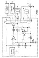
- FIG. 1 A preferred embodiment of the invention is shown in FIG. 1. It employs only two pins, represented as voltage terminal 2 and trimming terminal 4. These two terminals give the user the flexibility of using the internal reference voltage, trimmed or untrimmed, or connecting an external reference voltage to an internal digital-to-analog converter (DAC), ADC or other circuit requiring a reference voltage.
- DAC digital-to-analog converter
- An internal voltage source 8 generates a reference voltage which is brought out on lead 10.
- the internal reference voltage source may be implemented in several conventional ways, such as a bandgap voltage reference or a zener diode reference.
- a supply voltage V+ at supply voltage pin 14 would be +15 volts
- the voltage source 8 would generate 5 volts
- 10V would be the output voltage at terminal 2 when the trimming voltage is below an interrupting level to be described later.
- the voltage at terminal 2 is controlled by the open loop gain of an amplifier A1, a feedback network comprising transistor T1 and internal resistors R3 and R6, a resistor R2 connected between the R3/R6 junction and trimming terminal 4, and an external variable resistor 16.
- R3 and R6 typically 20 kilohms each
- a 5 volt reference applied to the amplifier's non-inverting input would yield 10 volts at terminal 2.
- This voltage is then trimmable by either adding or subtracting a small current through R3, from a potentiometer 16.
- a typical value for R2 would be 400 kilohms, and the variable reistor should be of the order of 100 kilohms.
- the open loop gain of the amplifier should be enough to overcome the voltage drop incurred by R1 and the base- emitter of T1, and still regulate terminal 2 to 12-bit accuracy.
- the reference voltage output level at terminal 2 is tied to the internal source 8 through the intervening circuit elements.
- a trimming voltage can be applied to trimming terminal 4 to adjust the output voltage level on terminal 2, in case it is not at the desired reference level because of circuit tolerances.
- Trimming terminal 4 is connected to the inverting input of op amp A1 through a resistor R2; another resistor R3 provides a feedback element between the emitter of transistor T1 and the inverting input of op amp A1.
- the output of op amp A1 can be adjusted to provide the desired voltage level at output terminal 2.
- the trimming voltage applied to terminal 4 can be derived in a conventional manner from potentiometer 16, which is fed by some convenient voltage supply such as output terminal 2 itself. It is an advantage of the present invention that it permits potentiometer 16 to be replaced with a digital-to-analog converter 18, shown connected to trimming terminal 4 by a dashed line connection, thus raising the reliability of the system.
- the circuit described thus far provides an internally generated, trimmed voltage at output terminal 2.
- the internal load such as one or more ADCs 6, a DAC, a comparator, an analog multiplier or some other circuit requiring a reference voltage, with a voltage produced by an external voltage reference source 20.
- prior voltage references have this capability, they require an additional terminal or pin to receive the external voltage.
- an external voltage source can be accommodated without using up any more pins.
- a special interrupt circuit is provided which interrupts the connection between internal voltage source 8 and output terminal 2 when an external voltage is desired, thus leaving output terminal 2 free to accept the external voltage.
- the preferred form of the interrupt circuit includes a pnp transistor T2 whose emitter is connected to trimming terminal 4.
- the base of T2 is kept at a constant voltage level by a connection to a voltage divider circuit consisting of resistors R7 and R4, which are connected between V+ and ground.
- the collector of T2 is connected to the base of an npn transistor T3, the emitter of which is grounded and the collector of which is connected to the base of transistor T1.
- a resistor R5 is connected between the base and emitter of T3.
- Resistors R7 and R4 are selected such that transistor T2 is held off when the voltage at trimming terminal 4 (and thereby at the emitter of T2) is within the desired trimming voltage range, but is held closed in a conductive state when the voltage at trimming terminal 4 is within some specified interrupt range outside of the trimming voltage range. For example, if the trimming voltage is limited to a maximum of 10 volts, the voltage at the base of transistor T2 could be set at some value greater than 10 volts. In that case, transistor T2 will not become conductive until the voltage applied to trimming terminal 4 exceeds the base voltage of T2 (plus its base-emitter voltage drop). When T2 does become conductive it turns on transistor T3, which is turn grounds the base of transistor T1 to hold T1 non-conductive. This opens up the connection between internal voltage source 8 and output terminal 2 with a high impedance interruption, thereby permitting the output of external voltage reference source 20 to be applied directly to terminal 2. For a negative reference voltage, the circuit polarity would simply be reversed.
- a convenient way to place the circuit in an external voltage reference mode is to simply connect a lead, indicated by dashed line 22, between V+ terminal 14 and trimming terminal 4.
- V+ at 15 volts and a trimming voltage range of 0-10 volts
- the relative values of R7 and R4 can be selected to establish any desired threshold voltage between 10 and 15 volts (at trimming terminal 4) for turning on transistor T2.
- a substantial gap is preferably left between the maximum trimming voltage, and the threshold voltage at trimming terminal 4 that will convert the circuit to its external reference mode.
- Typical resistance values are provided in FIG. 1, but are not to be considered as limiting.
- output terminal 2 can at the same time be used as a voltage reference for an external load circuit 24. Since numerous variations and alternate embodiments will be apparent to those skilled in the art, it is intended that the invention be limited only in terms of the appended claims.
Landscapes
- Engineering & Computer Science (AREA)
- Physics & Mathematics (AREA)
- Electromagnetism (AREA)
- General Physics & Mathematics (AREA)
- Radar, Positioning & Navigation (AREA)
- Automation & Control Theory (AREA)
- Continuous-Control Power Sources That Use Transistors (AREA)
Applications Claiming Priority (2)
| Application Number | Priority Date | Filing Date | Title |
|---|---|---|---|
| US16930888A | 1988-03-17 | 1988-03-17 | |
| US169308 | 1988-03-17 |
Publications (2)
| Publication Number | Publication Date |
|---|---|
| EP0333353A2 true EP0333353A2 (fr) | 1989-09-20 |
| EP0333353A3 EP0333353A3 (fr) | 1991-10-23 |
Family
ID=22615117
Family Applications (1)
| Application Number | Title | Priority Date | Filing Date |
|---|---|---|---|
| EP19890302113 Ceased EP0333353A3 (fr) | 1988-03-17 | 1989-03-02 | Circuit tension de référence à mode double et méthode |
Country Status (2)
| Country | Link |
|---|---|
| EP (1) | EP0333353A3 (fr) |
| JP (1) | JPH01271812A (fr) |
Cited By (2)
| Publication number | Priority date | Publication date | Assignee | Title |
|---|---|---|---|---|
| WO1992007315A1 (fr) * | 1990-10-16 | 1992-04-30 | Siemens Automotive S.A. | Dispositif servant a etablir un courant dans une partie analogique d'un circuit logique et analogique integre |
| WO1993006540A1 (fr) * | 1991-09-25 | 1993-04-01 | Astec International Limited | Circuit de programmation lineaire pour convertisseurs de courant a tension de sortie reglable |
Citations (2)
| Publication number | Priority date | Publication date | Assignee | Title |
|---|---|---|---|---|
| GB2056805A (en) * | 1979-06-28 | 1981-03-18 | Nippon Electric Co | Integrated logic circuits |
| DE3710865A1 (de) * | 1986-04-01 | 1987-10-22 | Toshiba Kawasaki Kk | Halbleitervorrichtung |
Family Cites Families (2)
| Publication number | Priority date | Publication date | Assignee | Title |
|---|---|---|---|---|
| JPS5729916B2 (fr) * | 1973-08-04 | 1982-06-25 | ||
| JPS5999510A (ja) * | 1982-11-30 | 1984-06-08 | Fujitsu Ltd | 定電圧回路 |
-
1989
- 1989-03-02 EP EP19890302113 patent/EP0333353A3/fr not_active Ceased
- 1989-03-17 JP JP6579589A patent/JPH01271812A/ja active Pending
Patent Citations (2)
| Publication number | Priority date | Publication date | Assignee | Title |
|---|---|---|---|---|
| GB2056805A (en) * | 1979-06-28 | 1981-03-18 | Nippon Electric Co | Integrated logic circuits |
| DE3710865A1 (de) * | 1986-04-01 | 1987-10-22 | Toshiba Kawasaki Kk | Halbleitervorrichtung |
Non-Patent Citations (2)
| Title |
|---|
| ELECTRONICS, 13th April 1978, pages 99-105, New York, US; P. BROKAW: "I2L puts it all together for 10-bit a-d converter chip" * |
| WESCON CONFERENCE RECORD, North Hollywood, September 1977, pages 1-5; J. SIMMONS: "Microprocessor 8-bit D/A-converter" * |
Cited By (3)
| Publication number | Priority date | Publication date | Assignee | Title |
|---|---|---|---|---|
| WO1992007315A1 (fr) * | 1990-10-16 | 1992-04-30 | Siemens Automotive S.A. | Dispositif servant a etablir un courant dans une partie analogique d'un circuit logique et analogique integre |
| US5418488A (en) * | 1990-10-16 | 1995-05-23 | Siemens Automotive, S.A. | Device for establishing a current in an analog part of an integrated logic and analog circuit |
| WO1993006540A1 (fr) * | 1991-09-25 | 1993-04-01 | Astec International Limited | Circuit de programmation lineaire pour convertisseurs de courant a tension de sortie reglable |
Also Published As
| Publication number | Publication date |
|---|---|
| JPH01271812A (ja) | 1989-10-30 |
| EP0333353A3 (fr) | 1991-10-23 |
Similar Documents
| Publication | Publication Date | Title |
|---|---|---|
| CA2068219C (fr) | Source d'alimentation stabilisee a deux tensions d'entree | |
| EP0316781A1 (fr) | Régulateur de tension à deux entrées et à faible chute de tension | |
| JP2790364B2 (ja) | 基準電圧を供給する回路 | |
| JPH02220114A (ja) | 電圧安定器 | |
| US5225811A (en) | Temperature limit circuit with dual hysteresis | |
| US4801816A (en) | Generator of periodial signals, in particular for switch-mode power supplies | |
| US4933572A (en) | Dual mode voltage reference circuit and method | |
| US6249162B1 (en) | Hysteresis circuit | |
| US4668875A (en) | Waveshaping circuit | |
| JPS6151813B2 (fr) | ||
| US7091633B2 (en) | Current-limiting logic interface circuit | |
| US5703476A (en) | Reference voltage generator, having a double slope temperature characteristic, for a voltage regulator of an automotive alternator | |
| US4319094A (en) | Three-terminal power supply circuit for telephone set | |
| US5589792A (en) | Resistor programmable temperature switch | |
| US6356061B1 (en) | Fully integrated linear regulator with darlington bipolar output stage | |
| JPH0546571B2 (fr) | ||
| EP0333353A2 (fr) | Circuit tension de référence à mode double et méthode | |
| GB1601595A (en) | Window discriminator or voltage range sensor | |
| US4752700A (en) | Apparatus for pre-defining circuit characteristics | |
| JPH0525201B2 (fr) | ||
| GB2091962A (en) | Volume control circuit | |
| EP0116995B1 (fr) | Configuration de stabilisation de courant | |
| EP0410764A2 (fr) | Circuit comparateur | |
| EP0751451A1 (fr) | Générateur de tension de référence ayant une caractéristique en température à double pente pour un régulateur de tension d'un alternateur d'automobile | |
| EP0343553B1 (fr) | Circuit électronique en veilleuse avec interruption à retard, commandé par basse tension |
Legal Events
| Date | Code | Title | Description |
|---|---|---|---|
| PUAI | Public reference made under article 153(3) epc to a published international application that has entered the european phase |
Free format text: ORIGINAL CODE: 0009012 |
|
| AK | Designated contracting states |
Kind code of ref document: A2 Designated state(s): DE FR GB IT NL |
|
| PUAL | Search report despatched |
Free format text: ORIGINAL CODE: 0009013 |
|
| AK | Designated contracting states |
Kind code of ref document: A3 Designated state(s): DE FR GB IT NL |
|
| 17P | Request for examination filed |
Effective date: 19920323 |
|
| 17Q | First examination report despatched |
Effective date: 19930923 |
|
| STAA | Information on the status of an ep patent application or granted ep patent |
Free format text: STATUS: THE APPLICATION HAS BEEN REFUSED |
|
| 18R | Application refused |
Effective date: 19940721 |