EP0333319A2 - Sammelleitungsverträgliche programmierbare Folgesteuerung - Google Patents
Sammelleitungsverträgliche programmierbare Folgesteuerung Download PDFInfo
- Publication number
- EP0333319A2 EP0333319A2 EP89301379A EP89301379A EP0333319A2 EP 0333319 A2 EP0333319 A2 EP 0333319A2 EP 89301379 A EP89301379 A EP 89301379A EP 89301379 A EP89301379 A EP 89301379A EP 0333319 A2 EP0333319 A2 EP 0333319A2
- Authority
- EP
- European Patent Office
- Prior art keywords
- register
- signals
- programmable sequencer
- bus
- wcs
- Prior art date
- Legal status (The legal status is an assumption and is not a legal conclusion. Google has not performed a legal analysis and makes no representation as to the accuracy of the status listed.)
- Granted
Links
Images

Classifications
-
- G—PHYSICS
- G06—COMPUTING OR CALCULATING; COUNTING
- G06F—ELECTRIC DIGITAL DATA PROCESSING
- G06F13/00—Interconnection of, or transfer of information or other signals between, memories, input/output devices or central processing units
- G06F13/38—Information transfer, e.g. on bus
- G06F13/382—Information transfer, e.g. on bus using universal interface adapter
- G06F13/385—Information transfer, e.g. on bus using universal interface adapter for adaptation of a particular data processing system to different peripheral devices
-
- G—PHYSICS
- G05—CONTROLLING; REGULATING
- G05B—CONTROL OR REGULATING SYSTEMS IN GENERAL; FUNCTIONAL ELEMENTS OF SUCH SYSTEMS; MONITORING OR TESTING ARRANGEMENTS FOR SUCH SYSTEMS OR ELEMENTS
- G05B2219/00—Program-control systems
- G05B2219/20—Pc systems
- G05B2219/22—Pc multi processor system
- G05B2219/2207—Microcontroller combined with state sequencer
Definitions
- This invention relates generally to digital controllers known as sequencers or state machines, and more particularly, to single-chip programmable digital sequencers having an on-chip interface to an external microprocessor.
- sequencers which operate autonomously with only condition codes to control program flow.
- One such sequencer is manufactured as an integrated circuit by Advanced Micro Devices, Inc. and designated the Am29PL141.
- This integrated circuit has an on-chip read-only memory which can store a "control program”.
- An advance over the Am29PL141 is described in the related, co-pending application "Programmable, Expandable Controller With Flexible I/O” and such description is incorporated by reference herein.
- the advance includes the provision of an on-chip memory which is a random access memory (RAM) type.
- the RAM is used to store "microinstructions" which form a control program for the sequencer.
- the control program can be dynamically altered which provides some external control over the sequencer.
- the sequencer should be accessible to an external microprocessor so that a wide variety of status conditions can be monitored by the microprocessor. Changes in the control program can then be dynamically made based on these status conditions internal to the sequencer as well as conditions external to the sequencer which are sensed by the microprocessor.
- An interface preferably integral to the integrated circuit housing the sequencer, should enable one of a number of commonly-used microprocessors to be connected to the intergrated circuit.
- a single-chip sequencer having a bidirectional bus compatible with a number of common microprocessors.
- the bus terminates on a set of pins of the chip housing the sequencer.
- Standard signals are applied to pins of the chip which permit reading and writing of information by the microprocessor to various elements of the sequencer.
- a writeable control store WCS which contains one or more control programs for the sequencer.
- the status of various registers, a stack, a program counter, a pipeline register used for the WCS, and several user-registers, among others, can be accessed by the microprocessor.
- the single-chip bus-compatible sequencer disclosed herein requires no external control store or other support circuitry.
- a microprocessor can be connected to the chip with little or no logic circuitry.
- the sequencer operates in either of two modes: one mode employs a read strobe and a write strobe for reading and writing by the microprocessor and is compatible then with microprocessors manufactured by the Intel Corporation. In a second mode the sequencer employs a data strobe and the direction of transfer on the bus is set by a read/write input signal. In this mode the sequencer is compatible with microprocessors manufactured by the Motorola Corporation.
- the sequencer provides a mechanism for detecting which type of microprocessor is connected to it and can automatically set the mode for compatibility with that particular microprocessor.
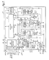
- Fig. 1 illustrates a typical application of a sequencer 10 according to the instant invention, connected to a microprocessor 8 and an object to be controlled 9 by the sequencer 10.
- D7-D0 form bidirectional data bus 12 and are active high three-state, bidirectional bus for transfer of data to and from a microprocessor.
- D/ ⁇ [Data/ ⁇ Address] 14 input for differentiating between Data and Address transfers.
- This signal line would normally be connected to the least significant address line of the host microprocessor bus in order to simplify control of communications.
- ⁇ CS [Chip Select] 16 is an active low input which enables a transfer to begin between the sequencer 10 and the host microprocessor.
- ⁇ RD [Read (Mode 0)] or ⁇ DS [Data Strobe (Mode 1)] 18 is dependent on the mode to which the sequencer 10 has been set (after the first write cycle in the case of mode 1).
- mode 0 the pin connected to line 18 behaves as a read strobe, and a read access is performed when it is received.
- mode 1 the pin behaves as a data strobe and a read or write access is performed depending on the state of the R/ ⁇ W line.
- ⁇ WR [Write (Mode 0)] or R/ ⁇ W [Read/Write (Mode 1)] 20 depends on the mode to which the sequencer 10 has been set (after the first write cycle in the case of mode one).
- mode 0 the pin connected to line 20 behaves as a write strobe, and a write access is performed when it is received.
- mode 1 the pin behaves as a read/write indicator.
- INT [Interrupt] 22 is an active high output that provides an interrupt to the host microprocessor when one or more interrupt mask registers bits are unmasked and the relevant status bit(s) become active.
- I/O15-I/O0 is a bidirectional Input/Output bus 24: as an Output is connected to an internal writable control store (WCS) via a pipeline register. These pins can be individually reconfigured as registered inputs by changing the contents of an Output Disable (O_DIS) register appropriately.
- WCS writable control store
- ⁇ OE [Output enable] 26 is an active low input to enable the relevent bits of the Output bus which are not masked by an Output Mask (O_MSK) register, or disabled by the O_DIS register.
- O_MSK Output Mask
- T7-T0 [Test Inputs] 28 are a set of eight test inputs which are used to conditionally control the flow of the microprogram in the sequencer 10. The polarity of the test is programmable by a bit in the micro code. These inputs are registered.
- ⁇ INT [Micro-interrupt] 30 is a low-to-high edge triggered input to indicate that a micro-interrupt routine should be executed.
- WCS bit 43 in the micro code in conjunction with a Control 1 Register bit 0, enables or disables this interrupt. After an interrupt has been recognized, no further interrupts are recognized until after the first instruction of the current interrupt has been executed. If interrupts are enabled, there is a synchronization latency of at least 1 cycle, and at most 2 cycles, from the rising edge of ⁇ INT to the first cycle of the interrupt routine.
- ⁇ RESET ( ⁇ RES) 32 is an active low input that causes a reset of the sequencer 10.
- CLK [Clock] 34 is an input that supplies a synchronizer clock for all elements of sequencer 10 except for a bus interface control block 36.
- Fig. 2 is a block diagram of a sequencer 10 in accordance with the instant invention.
- the sequencer 10 depicted in Fig. 2 is preferably fabricated as a single monolithic integrated circuit (chip). Access to the elements within the boundary of the chip is via terminals (pins) of the chip. Signal lines crossing the boundary of the chip shown on the left side of Fig. 2 are among those lines connected to the pins. Signal lines shown in Fig. 2 have a number adjacent to a slash through the signal line. This number indicates the number of conductors comprising the signal line and allows that number of signals to be conducted in parallel.
- a bus interface control 36 receives the D/ A , CS , RD ( DS ) and WR (R/ W ) signals from the host microprocessor and generates the INT signal thereto, if an interrupt condition occurs and is unmasked.
- the bus interface control 36 is connected to data bus 12 via a set of control lines 38.
- the structure and operation of the bus interface control 36 is conventional in all respects except for the automatic configuration into mode 0 or 1 which allows bus 12 compatibility with Intel or Motorola microprocessors, respectively. This aspect of the invention is described in the related co-pending application "Universal Microprocessor Interface", and such description is incorporated by reference herein.
- bus interface control 36 will not be described herein since it is conventional and known to those of ordinary skill in the art.
- a register file 40 contains a variety of registers accessible to the host microprocessor via data bus 12. A description of register file 40 will be given hereinbelow in connection with Fig. 2. An address register 41 is used in conjunction with register file 40 and will likewise be described in connection with Fig. 2.
- the register file 40 is seen by the host microprocessor as a single set of addressable registers, organized as a file. However, the register file 40 is implemented to permit the sequencer 10 access to the contents of the various registers and to allow modification of the contents of more than one register therein during a single cycle of the sequencer.
- Fig. 2 The remaining elements shown in Fig. 2 and denoted generally by reference numeral 11, other than a Mask Logic 42, a register 43, a multiplexer (MUX) 44, and a tri-state buffer 45, are described in the related, co-pending application "Programmable, Expandable Controller With Flexible I/O" and such description is incorporated by reference herein. Particular attention is drawn to the block diagram of Fig. 11 in that related application, which is similar in all important respects to that portion of Fig. 2 labelled by numeral II, other than as described above.
- Mask Logic 42 and tri-state buffers 45 permit terminal pins 24 to operate as either input or output terminals, as determined by the OE signal on line 26 and a microinstruction stored in WCS 52.
- This aspect of the sequencer 10 is described in the related, co-pending application entitled “Flexible, Reconfigurable Terminal Pin", and such description is incorporated herein by reference.
- Register file 40 includes four user registers (USERO, USER1, USER2 and USER3) which are accessible via a bus 45 by elements of sequencer 10.
- a bus 46 interconnects the register file 40 and inputs to a PC MUX 48.
- a bus 50 conducts a writeable control store (WCS) address from register file 40 to WCS 52 and to a bidirectional multiplexer (MUX) 54.
- WCS writeable control store
- MUX bidirectional multiplexer
- the MUX 54 also is connected to register file 40 by a bidirectional bus 56 conducting WCS data to and from WCS 52.
- the writable control store (WCS) 52 is preferably arranged as 256 words each of 45 bits. It is accessed by the microprocessor via the bus interface control block 36, which reads or writes six bytes for each word of the micro code.
- the output of the WCS 52 is pipelined (via pipeline register 57) and the word separated into seven fields depending on an instruction format.
- Sixteen bits of the micro code word (0-15) are output on signal lines 24 from the sequencer via three-state buffers 45.
- the upper byte can be replaced by the output of the PC-MUX by setting bit 0 of a Control 2 register (Enable ⁇ PC), and the lower byte can be replaced with the lower 8 bits of the counter by setting bit 1 of the Control 2 register (or by executing a TXC instruction).
- all 16 output bits can be replaced by the contents of one of the User registers by executing a TXU instruction.
- any of these output pins can be individually reconfigured as an input pin by setting a O_DIS register appropriately.
- Sixteen bits of the micro code word (31-16) form a data field which is used for various functions, such as branch addresses or user register addresses.
- the lower 8 bits of this field may be used for data while the upper 8 bits are used as a Mask value.
- the upper 8 bits are used as a Mask value, while the 2 LSBs are used as a User Register Select field and the other 6 bits are unused.
- the 2 LSBs are used as the User Register Select field while the remaining 14 bits are unused.
- One bit of the micro code (36) selects the polarity of the test (true or false) for use with the Test field. Alternatively, it is combined with the 4 bits of the Test field to make up a Register Select field.
- micro code word (43) enables micro-interrupts when set, but it can be overridden by bit 0 of the Control 1 register. This allows the user to have, for example, a subroutine which normally enables interrupts but which, when called from certain places in the program, has its ability to enable interrupts blocked.
- One bit of the micro code word (44) enables the relevent bits of the Output buffers which are not masked by the WCS_OE registers or diabled by the O_DIS register.
- the address register 41 is accessed by the microprocessor when the D/ ⁇ A signal is LOW; otherwise the microprocessor is connected to data registers within register file 40.
- the contents of address register 41 conducted to register file 40 on bus 58 determines which data register is to be accessed by the microprocessor, in accordance with Table I.
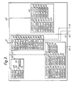
- Register File 40 is shown in block diagram form. Register File 40 consists of four groups of registers: read-only registers (ROM REGS) 60, Writeable Control Store registers (WCS REGS) 62, Sequencer Interface Registers 64, and Sequencer Diagnostic Registers 66.
- ROM REGS read-only registers
- WCS REGS Writeable Control Store registers
- Sequencer Interface Registers 64 Sequencer Diagnostic Registers 66.
- ROM Registers provide information about the sequencer to the host microprocessor.
- MAN_ID 68 contains the manufacturer's identity code.
- REV 70 contains the revision number.
- PART 72, 74 contain the device part number.
- the Status Register 76 serves as the source of interrupts to the host processor, enables the host to establish the cause of an interrupt or to poll the status of the sequencer 10. Each of the bits in this register can generate an interrupt to the host when they are set, if their corresponding mask bit in an Int_Mask register is cleared. While the Status Register is not strictly a ROM location, it is included in this group because it is not setable by the host processor. Instead, writing ones to the status register serves to clear the appropriate bits. For example, if 0000 0001 is written to the Status Register, then the I0 flag (or interrupt) is cleared and all the other bits are unchanged.
- the Status Register 76 contains seven bits which are defined as follows:
- a HALT bit indicates that the sequencer has executed a halt instruction. It is not set when the sequencer is halted by the host microprocessor through the Halt bit in a mode register;
- a BREAK bit indicates that the sequencer has reached a breakpoint
- An A_FULL bit indicates that the sequencer stack has 28 or more entries in it, and that some action may need to be taken to avoid a possible stack overflow
- a SEQ_LD bit indicates that the sequencer has caused one of the user registers to be loaded
- a SEQ_INT bit indicates that the INT instruction has been executed by the sequencer
- a ⁇ INT bit indicates that the micro-interrupt line has been asserted
- An I0 bit indicates the selected test input has been asserted. The selection is made with bits 0 to 2 of a Test_Sel register, and the polarity is selected by bit 7 of the Test_Sel register.
- the Writable Control Store Registers 62 group of registers are the means by which the host microprocessor can access the writable control store 52 and control its contents. All these registers can be read and written by the microprocessor.
- a WCS Address (WCS_A) register 78 holds the address of a micro-word in the WCS 52.
- the host microprocessor To read or write a full word of the WCS, the host microprocessor must read or write 6 bytes of data. When 6 bytes of data have been read or written, the WCS_A register is automatically incremented. This operation is achieved by means of a 3 bit counter (not shown) which is cleared by a write to the WCS address register 78 and which counts in modulo 6 fashion thereafter so as to multiplex the bytes into the proper position in the WCS word (the low order byte is the first byte read or written). To send a block of data, the host microprocessor sets up the base address by writing to the WCS address register 78 and then sends micro-code words in multiples of 6 bytes to a WCS data register 80.
- the WCS_Data (WCS_D) register 80 is the means by which the host microprocessor writes or reads the WCS 52.
- a Test Group 1 (TESTG_1) Register 82 and a Test Group 2 (TESTG_2) Register 84 contain bit patterns indicative of which of the TEST signals 28, or internal signals is selected by the TEST MUX, and is to be tested by a particular microinstruction.
- a CONTROL1 register 86 holds the micro-interrupt enable bit ( ⁇ IEN, bit 0). This bit operates in conjunction with bit 42 of the WCS as shown below.
- CONTROL REGISTER BITS Control 1 ⁇ IEN (bit 0) WCS ⁇ IEN (bit 42) Result: Interrupts are: 1 0 Ignored 1 1 Accepted 0 x Ignored
- an EQ bit which allows the state of the EQ flag to be saved and restored in the event of an interrupt. This bit can be read to obtain the current state and can be set or cleared as desired in order to restore it.
- a CONTROL2 register 88 contains a:
- Bit 0 (EN_ ⁇ PC) which when set, places the 8 bit value of the micro-code address on the upper byte of the input/output lines 24;
- Bit 2 (BRK Match Report bit) which when set, causes the interrupt pin to output the break match logic status so that when a breakpoint match occurs, it is driven high for the duration of the instruction.
- the sequencer continues to run without halting. This is useful when a trigger is desired on the occurrence of the breakpoint but the sequencer should not be halted, as might be the case for oscilloscope-loop type diagnostics.
- this bit When this bit is on, all normal sources of interrupt are blocked, as if EN_INT in the Mode register was set to zero. The BRKEN bit in the Mode register is also ignored.
- An OE_MSK register comprising an OE_MSK L register 90 and an OE_MSK H register 92 provides a mask which determines which bits of the Output bus 24 are affected by the ⁇ OE input signal on line 26. Output bits are three-stated by the ⁇ OE pin only if bits in the mask register 90, 92 are set to a '1'. Since the ⁇ OE signal is a low-true input, the ⁇ OE pin can only three-state the relevant bits of I/O bus 24 when it is a '1' as well.
- a WCS_OE register comprising a WCS_OEL register 94 and a WCS_OEH register 96 performs a similar function to that of the OE_MSK register.
- the WCS_OE register masks bits of the Output bus 24 which are to be three-stated by the ⁇ OE bit in the micro-word. Output bits are three-stated by the ⁇ OE bit in the micro code only if bits in the WCS_OE register are set to a '1'. Since the ⁇ OE bit is an active low micro-code bit, the ⁇ OE bit can only three-state the relevant bits of the bus when it is a '1' as well.
- An Output Disable (O_DIS) register comprising an O_DIS_ L register 98 and an O_DIS_ H register 100 is a mask register similar to the two previous mask registers in that it selects which pins will be enabled as outputs. The difference is that while WCS_OE and OE_MASK can allow pins to be selectively enabled, O_DIS forces pins to be always disabled, allowing them to be used as additional test inputs. This disabling function overrides the function of the WCS_OE, OE_MASK, EN_ ⁇ PC, and EN_TXC. When a bit in this register is set, the corresponding output is disabled.
- the Sequencer Interface Block of registers 64 is the means by which the host microprocessor may affect the sequence of micro code executed. These registers can all be read and written by the microprocessor.
- An Interrupt mask (INT_MASK) register 102 is used to mask off unwanted interrupts to the host microprocessor.
- the bits positions correspond directly to bits in the Status register 76 described hereinabove. To enable an interrupt the relevant bit should be cleared.
- the host microprocessor receives an interrupt it can read the Status Register 76 to determine from the bit pattern which of several possible interrupts actually occurred. Upon learning which interrupt occurred, the host microprocessor can then write a 1 to the corresponding bit in the Status register to reset it while leaving all the other interrupt bits unaffected.
- An enabled interrupt will continue to be asserted to the host processor until the host does one of three things:
- a BRKPOINT register 104 allows the sequencer to stop (or generate an interrupt) at a particular point in the micro code.
- a breakpoint can be set by writing an address into the breakpoint register. When the breakpoint is reached, bit 6 of the Status register 76 is set and the appropriate action taken (halt or interrupt). This register is read/write.
- the micro-interrupt vector ( ⁇ INT_VECT) register 106 specifies the address for micro-interrupts (interrupts to the sequencer). When micro-interrupts are enabled and an interrupt occurs, this register supplies the starting address of the micro-interrupt service routine. The interrupt return address is pushed onto the stack while the first instruction of interrupt service routine is being executed. This register is read/write.
- a mode register 108 controls the global operation of the sequencer; such as start, halt, stop at breakpoint and reset.
- This register is read/write. It contains a START bit, which when set, allows the sequencer to execute micro code. This bit must be set after a reset condition, or after the sequencer is halted or a breakpoint has occurred, in order to start or restart the sequencer. However, if a Halt bit in the Mode register has been set but not yet cleared, then setting the start bit will cause the sequencer to perform a single step operation. The Halt bit in the Status register has no effect on the restarting of the sequencer.
- a ⁇ HALT bit when set, halts the sequencer after the current cycle. The contents of all registers will be maintained.
- the microprocessor may change values in the sequencer (e.g., for debugging) and restart the sequencer. The microprocessor may also use this bit to halt the sequencer in the event of a micro code failure. This bit allows a single-step mode since a Start will cause the sequencer to halt again after only one instruction has been executed.
- a BRKEN bit when set, enables the breakpoint facility.
- the host microprocessor writes an 8-bit address into the breakpoint register 104 and when the ⁇ PC address equals the breakpoint register value, the sequencer will stop on the next cycle, unless the BRK_Match_Report bit (Control register 2 bit 2) is set, in which came an interrupt will be generated instead.
- a EN_INT bit when set, allows the sequencer to interrupt the host microprocessor when one or more of the interrupt conditions occur. It is ignored if the BRK_Match_Report bit 2 of the Control register 2 is set.
- a SINGLE_STEP_DONE bit is set by any successfully run sequencer cycle, and will therefore be always on during normal execution.
- a RESET bit when set, will initiate a software reset of the sequencer.
- a 1 indicates that the device is in the process of performing a reset. This bit automatically returns to 0 when the reset operation is complete.
- a Test register 110 when read, indicates the value of the registered Test inputs on line 28.
- An IOTEST comprising an IOTEST L register 112 and an IOTEST H register 114 forms a 16 bit register which holds the synchronized value of the I/O pins on bus 24. If any of these I/O pins have been selected as inputs by the O_DIS register 98, 100 then the contents of the IOTEST register can be used as test inputs, as selected by the Test Group 2 register 84.
- U_TEST register 116 contains four bits which are set by the microprocessor and accordingly user defined.
- a WRT_FLGS register 118 allows access to four semaphore flags. These flags are set whenever a write to the corresponding User register (high byte only) has taken place from either the sequencer or the host microprocessor. The are cleared whenever either the sequencer or the microprocessor reads the high byte of the register.
- a Test Select (TEST_SEL) register 120 is used to select one of the 8 registered Test input pins to serve as the I0 input to the Status register 76 and so be capable of causing an interrupt to the host microprocessor.
- An I0 Pol bit is used to select the polarity of the test inputs for use as an interrupt. If I0 Pol is 0 then a low to high transition on the selected registered test input can cause an interrupt. If I0 Pol is 1, then a high to low transition is required to cause an interrupt. For either case, I0 interrupts only occur if the I0 mask bit in the Int_Mask register is clear.
- USER [0:3] are four 16-bit user defineable registers comprising a low-order register 122, 126, 130, 134 and a high-order register 124, 128, 132 and 136, respectively, which can be read and written by both the host microprocessor and the sequencer.
- the sequencer can use the contents of these registers as branch addresses and data values.
- the corresponding W flag (Write Flag) in register 118 is also set. This allows either the host microprocessor or the sequencer to sense that the other has written something into a User register, which it can now read as necessary, so that these flags serve as a semaphore communication system between the processors.
- a flag is cleared by either the microprocessor or the sequencer reading the high byte of the appropriate register.
- Sequencer Diagnostic Registers 66 enable the host microprocessor to read or write the sequencer registers. This is especially useful for testing and debugging micro code.
- a ⁇ PC Register 142 contains the value of the Program Counter of the sequencer.
- a STCK_PTR Register 144 contains the value of the stack pointer. After a stack pointer reset, the value in STCK_PTR register 144 is set to zero; a pro-increment is performed on a Push operation prior to writing the top of the stack and a post-decrement is performed after the top of the stack is read.
- a TOS register comprising a low-order register 146 and a high-order register 148 contains the 16-bit value currently in the top of stack register of the sequencer.
- a COUNT register comprising a low-order register 150 and a high-order register 152 contains the 16-bit value currently in the counter of the sequencer.
- a RO_STK register comprising a low-order register 153a and a high-order register 153b contains the 16-bit value currently in the stack of the sequencer.
- a PIPE register comprising six registers 154, 156, 158, 160, 162 and 164 contains the 45-bit value currently in the WCS pipeline register 57 (6 bytes, written or read one byte at a time, starting with the low order byte).
- the ability to read or write this register allows the user the ability, for example, to force a particular instruction to be executed by halting the sequencer, writing a new value into the pipeline register 57, and then restarting the sequencer.
Landscapes
- Engineering & Computer Science (AREA)
- Theoretical Computer Science (AREA)
- Physics & Mathematics (AREA)
- General Engineering & Computer Science (AREA)
- General Physics & Mathematics (AREA)
- Debugging And Monitoring (AREA)
- Information Transfer Systems (AREA)
- Communication Control (AREA)
- Executing Machine-Instructions (AREA)
- Programmable Controllers (AREA)
Applications Claiming Priority (2)
| Application Number | Priority Date | Filing Date | Title |
|---|---|---|---|
| US167598 | 1988-03-14 | ||
| US07/167,598 US4967346A (en) | 1988-03-14 | 1988-03-14 | Universal microprocessor interface circuit |
Publications (3)
| Publication Number | Publication Date |
|---|---|
| EP0333319A2 true EP0333319A2 (de) | 1989-09-20 |
| EP0333319A3 EP0333319A3 (de) | 1993-01-07 |
| EP0333319B1 EP0333319B1 (de) | 1997-05-21 |
Family
ID=22608013
Family Applications (2)
| Application Number | Title | Priority Date | Filing Date |
|---|---|---|---|
| EP89301377A Ceased EP0333318A3 (de) | 1988-03-14 | 1989-02-14 | Schnittstellenschaltungen für einen Mikroprozessor |
| EP89301379A Expired - Lifetime EP0333319B1 (de) | 1988-03-14 | 1989-02-14 | Sammelleitungsverträgliche programmierbare Folgesteuerung |
Family Applications Before (1)
| Application Number | Title | Priority Date | Filing Date |
|---|---|---|---|
| EP89301377A Ceased EP0333318A3 (de) | 1988-03-14 | 1989-02-14 | Schnittstellenschaltungen für einen Mikroprozessor |
Country Status (5)
| Country | Link |
|---|---|
| US (1) | US4967346A (de) |
| EP (2) | EP0333318A3 (de) |
| JP (1) | JPH0214349A (de) |
| AT (1) | ATE153458T1 (de) |
| DE (1) | DE68928052D1 (de) |
Cited By (1)
| Publication number | Priority date | Publication date | Assignee | Title |
|---|---|---|---|---|
| EP0423036A3 (en) * | 1989-10-11 | 1991-09-25 | Bull Micral Of America, Inc. | Cpu-bus controller |
Families Citing this family (27)
| Publication number | Priority date | Publication date | Assignee | Title |
|---|---|---|---|---|
| JPH0235524A (ja) * | 1988-03-14 | 1990-02-06 | Advanced Micro Devicds Inc | バスコンパチブルプログラマブルシーケンサ |
| US5163145A (en) * | 1989-04-25 | 1992-11-10 | Dell Usa L.P. | Circuit for determining between a first or second type CPU at reset by examining upper M bits of initial memory reference |
| US5297272A (en) * | 1989-08-02 | 1994-03-22 | Advanced Logic Research, Inc. | Apparatus for automatically disabling and isolating a computer's original processor upon installation of a processor upgrade card |
| US5155839A (en) * | 1989-09-29 | 1992-10-13 | Allen-Bradley Company, Inc. | Apparatus using in undifferentiated strobe output to interface either of two incompatible memory access signal types to a memory |
| JP2559868B2 (ja) * | 1990-01-06 | 1996-12-04 | 富士通株式会社 | 情報処理装置 |
| GB9018991D0 (en) * | 1990-08-31 | 1990-10-17 | Ncr Co | Work station with timing independant interface units |
| WO1992006433A1 (en) * | 1990-10-03 | 1992-04-16 | Allied-Signal Inc. | Universal processor interface component |
| US5761479A (en) * | 1991-04-22 | 1998-06-02 | Acer Incorporated | Upgradeable/downgradeable central processing unit chip computer systems |
| EP0510241A3 (en) * | 1991-04-22 | 1993-01-13 | Acer Incorporated | Upgradeable/downgradeable computer |
| US5551012A (en) * | 1991-04-22 | 1996-08-27 | Acer Incorporated | Single socket upgradeable computer motherboard with automatic detection and socket reconfiguration for inserted CPU chip |
| US5495594A (en) * | 1991-07-12 | 1996-02-27 | Zilog, Inc. | Technique for automatically adapting a peripheral integrated circuit for operation with a variety of microprocessor control signal protocols |
| EP0529142A1 (de) * | 1991-08-30 | 1993-03-03 | Acer Incorporated | Ausbaubare und abbaubare Rechner |
| KR930006553A (ko) * | 1991-09-27 | 1993-04-21 | 리차드 이. 살웬 | 디지탈 컴퓨터 시스템 |
| KR950002162B1 (ko) * | 1992-02-12 | 1995-03-14 | 삼성전자주식회사 | Cpu 로직의 자동 절환 장치 |
| US5790834A (en) * | 1992-08-31 | 1998-08-04 | Intel Corporation | Apparatus and method using an ID instruction to identify a computer microprocessor |
| US5440702A (en) * | 1992-10-16 | 1995-08-08 | Delco Electronics Corporation | Data processing system with condition code architecture for executing single instruction range checking and limiting operations |
| US5490279A (en) * | 1993-05-21 | 1996-02-06 | Intel Corporation | Method and apparatus for operating a single CPU computer system as a multiprocessor system |
| US5884091A (en) * | 1993-12-08 | 1999-03-16 | Intel Corporation | Computer system having a central processing unit responsive to the identity of an upgrade processor |
| AU2821395A (en) * | 1994-06-29 | 1996-01-25 | Intel Corporation | Processor that indicates system bus ownership in an upgradable multiprocessor computer system |
| US5734872A (en) * | 1994-09-19 | 1998-03-31 | Kelly; Michael | CPU interconnect system for a computer |
| US6038400A (en) * | 1995-09-27 | 2000-03-14 | Linear Technology Corporation | Self-configuring interface circuitry, including circuitry for identifying a protocol used to send signals to the interface circuitry, and circuitry for receiving the signals using the identified protocol |
| US5862351A (en) * | 1996-11-07 | 1999-01-19 | He; Zhi Qiang | Motherboard with automatic configuration |
| WO2000052592A2 (en) * | 1999-02-28 | 2000-09-08 | Embedded Planet Llc | Computer circuit for families of processors |
| US6772328B1 (en) * | 1999-06-18 | 2004-08-03 | Samsung Electronics Co., Ltd. | Dynamic initialization of processor module via motherboard interface |
| US6985987B2 (en) * | 2000-11-01 | 2006-01-10 | Via Technologies, Inc. | Apparatus and method for supporting multi-processors and motherboard of the same |
| US6842816B1 (en) * | 2001-07-31 | 2005-01-11 | Network Elements, Inc. | Configurable glueless microprocessor interface |
| US20040008725A1 (en) * | 2002-07-15 | 2004-01-15 | Analog Devices, Inc. | Method and an interface circuit configurable in two communication protocol modes |
Family Cites Families (3)
| Publication number | Priority date | Publication date | Assignee | Title |
|---|---|---|---|---|
| US4287563A (en) * | 1979-11-13 | 1981-09-01 | Motorola, Inc. | Versatile microprocessor bus interface |
| US4379327A (en) * | 1980-07-21 | 1983-04-05 | Motorola, Inc. | Universal interface circuit for synchronous and asynchronous buses |
| US4641261A (en) * | 1984-05-21 | 1987-02-03 | Rca Corporation | Universal interface circuit for microprocessor peripherals |
-
1988
- 1988-03-14 US US07/167,598 patent/US4967346A/en not_active Expired - Lifetime
-
1989
- 1989-02-14 EP EP89301377A patent/EP0333318A3/de not_active Ceased
- 1989-02-14 EP EP89301379A patent/EP0333319B1/de not_active Expired - Lifetime
- 1989-02-14 DE DE68928052T patent/DE68928052D1/de not_active Expired - Lifetime
- 1989-02-14 AT AT89301379T patent/ATE153458T1/de not_active IP Right Cessation
- 1989-03-13 JP JP1061971A patent/JPH0214349A/ja active Pending
Cited By (1)
| Publication number | Priority date | Publication date | Assignee | Title |
|---|---|---|---|---|
| EP0423036A3 (en) * | 1989-10-11 | 1991-09-25 | Bull Micral Of America, Inc. | Cpu-bus controller |
Also Published As
| Publication number | Publication date |
|---|---|
| EP0333319A3 (de) | 1993-01-07 |
| ATE153458T1 (de) | 1997-06-15 |
| DE68928052D1 (de) | 1997-06-26 |
| US4967346A (en) | 1990-10-30 |
| JPH0214349A (ja) | 1990-01-18 |
| EP0333318A2 (de) | 1989-09-20 |
| EP0333318A3 (de) | 1990-08-01 |
| EP0333319B1 (de) | 1997-05-21 |
Similar Documents
| Publication | Publication Date | Title |
|---|---|---|
| EP0333319A2 (de) | Sammelleitungsverträgliche programmierbare Folgesteuerung | |
| US4670838A (en) | Single chip microcomputer capable of debugging an external program without an increase of the number of terminals/ports | |
| US5826093A (en) | Dual function disk drive integrated circuit for master mode and slave mode operations | |
| EP0720093A1 (de) | Mikroprozessor mit Fehlersuchsystem | |
| US5031091A (en) | Channel control system having device control block and corresponding device control word with channel command part and I/O command part | |
| US4271466A (en) | Direct memory access control system with byte/word control of data bus | |
| US4839797A (en) | Microprocessor compatible with any software represented by different types of instruction formats | |
| US4688166A (en) | Direct memory access controller supporting multiple input/output controllers and memory units | |
| EP0127440B1 (de) | Integrierter Schaltkreis mit einem eingebauten Datenverarbeitungsgerät und einem Festwertspeicher mit darin eingespeisten Anwendersprogrammen | |
| US4669059A (en) | Method and apparatus in a data processor for selectively disabling a power-down instruction | |
| US5042002A (en) | Programmable controller with a directed sequencer | |
| US4573117A (en) | Method and apparatus in a data processor for selectively disabling a power-down instruction | |
| US5717851A (en) | Breakpoint detection circuit in a data processor and method therefor | |
| JPS61241841A (ja) | エミユレ−タ | |
| US5367649A (en) | Programmable controller | |
| CA1036713A (en) | Peripheral interrupt priority resolution in a micro program data processor having plural levels of subinstruction sets | |
| US3742457A (en) | High speed data transfer for a peripheral controller | |
| EP0384570A2 (de) | Kompatibles, erweitertes, programmierbares Optionenauswahlsystem | |
| US5175831A (en) | System register initialization technique employing a non-volatile/read only memory | |
| US5553301A (en) | Programmable sequencher having internal components which are microprocessor read/write interfacable | |
| EP0712078A1 (de) | Verfahren und Datenprozessor zum durchsichtigem Betrieb in einem Hintergrundmodus | |
| JP2591181B2 (ja) | マイクロコンピュータ | |
| US5367641A (en) | MIL-STD-1553 interface device having a bus controller minor frame timer | |
| JPH02252008A (ja) | マイクロプロセッサ | |
| US4095268A (en) | System for stopping and restarting the operation of a data processor |
Legal Events
| Date | Code | Title | Description |
|---|---|---|---|
| PUAI | Public reference made under article 153(3) epc to a published international application that has entered the european phase |
Free format text: ORIGINAL CODE: 0009012 |
|
| AK | Designated contracting states |
Kind code of ref document: A2 Designated state(s): AT BE CH DE ES FR GB GR IT LI LU NL SE |
|
| PUAL | Search report despatched |
Free format text: ORIGINAL CODE: 0009013 |
|
| AK | Designated contracting states |
Kind code of ref document: A3 Designated state(s): AT BE CH DE ES FR GB GR IT LI LU NL SE |
|
| 17P | Request for examination filed |
Effective date: 19930617 |
|
| 17Q | First examination report despatched |
Effective date: 19941013 |
|
| GRAG | Despatch of communication of intention to grant |
Free format text: ORIGINAL CODE: EPIDOS AGRA |
|
| GRAH | Despatch of communication of intention to grant a patent |
Free format text: ORIGINAL CODE: EPIDOS IGRA |
|
| GRAH | Despatch of communication of intention to grant a patent |
Free format text: ORIGINAL CODE: EPIDOS IGRA |
|
| GRAA | (expected) grant |
Free format text: ORIGINAL CODE: 0009210 |
|
| AK | Designated contracting states |
Kind code of ref document: B1 Designated state(s): AT BE CH DE ES FR GB GR IT LI LU NL SE |
|
| PG25 | Lapsed in a contracting state [announced via postgrant information from national office to epo] |
Ref country code: IT Free format text: LAPSE BECAUSE OF FAILURE TO SUBMIT A TRANSLATION OF THE DESCRIPTION OR TO PAY THE FEE WITHIN THE PRE;WARNING: LAPSES OF ITALIAN PATENTS WITH EFFECTIVE DATE BEFORE 2007 MAY HAVE OCCURRED AT ANY TIME BEFORE 2007. THE CORRECT EFFECTIVE DATE MAY BE DIFFERENT FROM THE ONE RECORDED.SCRIBED TIME-LIMIT Effective date: 19970521 Ref country code: AT Effective date: 19970521 Ref country code: ES Free format text: THE PATENT HAS BEEN ANNULLED BY A DECISION OF A NATIONAL AUTHORITY Effective date: 19970521 Ref country code: FR Effective date: 19970521 Ref country code: CH Effective date: 19970521 Ref country code: BE Effective date: 19970521 Ref country code: GR Free format text: LAPSE BECAUSE OF FAILURE TO SUBMIT A TRANSLATION OF THE DESCRIPTION OR TO PAY THE FEE WITHIN THE PRESCRIBED TIME-LIMIT Effective date: 19970521 Ref country code: LI Effective date: 19970521 Ref country code: NL Free format text: LAPSE BECAUSE OF FAILURE TO SUBMIT A TRANSLATION OF THE DESCRIPTION OR TO PAY THE FEE WITHIN THE PRESCRIBED TIME-LIMIT Effective date: 19970521 |
|
| REF | Corresponds to: |
Ref document number: 153458 Country of ref document: AT Date of ref document: 19970615 Kind code of ref document: T |
|
| REG | Reference to a national code |
Ref country code: CH Ref legal event code: EP |
|
| REF | Corresponds to: |
Ref document number: 68928052 Country of ref document: DE Date of ref document: 19970626 |
|
| PG25 | Lapsed in a contracting state [announced via postgrant information from national office to epo] |
Ref country code: SE Effective date: 19970821 |
|
| PG25 | Lapsed in a contracting state [announced via postgrant information from national office to epo] |
Ref country code: DE Effective date: 19970822 |
|
| EN | Fr: translation not filed | ||
| NLV1 | Nl: lapsed or annulled due to failure to fulfill the requirements of art. 29p and 29m of the patents act | ||
| REG | Reference to a national code |
Ref country code: CH Ref legal event code: PL |
|
| PG25 | Lapsed in a contracting state [announced via postgrant information from national office to epo] |
Ref country code: LU Free format text: LAPSE BECAUSE OF NON-PAYMENT OF DUE FEES Effective date: 19980214 Ref country code: GB Free format text: LAPSE BECAUSE OF NON-PAYMENT OF DUE FEES Effective date: 19980214 |
|
| PLBE | No opposition filed within time limit |
Free format text: ORIGINAL CODE: 0009261 |
|
| STAA | Information on the status of an ep patent application or granted ep patent |
Free format text: STATUS: NO OPPOSITION FILED WITHIN TIME LIMIT |
|
| 26N | No opposition filed | ||
| GBPC | Gb: european patent ceased through non-payment of renewal fee |
Effective date: 19980214 |