EP0332218A2 - Verfahren zur Herstellung einer supraleitenden Schicht - Google Patents
Verfahren zur Herstellung einer supraleitenden Schicht Download PDFInfo
- Publication number
- EP0332218A2 EP0332218A2 EP89104323A EP89104323A EP0332218A2 EP 0332218 A2 EP0332218 A2 EP 0332218A2 EP 89104323 A EP89104323 A EP 89104323A EP 89104323 A EP89104323 A EP 89104323A EP 0332218 A2 EP0332218 A2 EP 0332218A2
- Authority
- EP
- European Patent Office
- Prior art keywords
- film
- superconductive
- ion milling
- produced
- present
- Prior art date
- Legal status (The legal status is an assumption and is not a legal conclusion. Google has not performed a legal analysis and makes no representation as to the accuracy of the status listed.)
- Withdrawn
Links
Images
Classifications
-
- H—ELECTRICITY
- H10—SEMICONDUCTOR DEVICES; ELECTRIC SOLID-STATE DEVICES NOT OTHERWISE PROVIDED FOR
- H10N—ELECTRIC SOLID-STATE DEVICES NOT OTHERWISE PROVIDED FOR
- H10N60/00—Superconducting devices
- H10N60/01—Manufacture or treatment
- H10N60/0268—Manufacture or treatment of devices comprising copper oxide
- H10N60/0661—Processes performed after copper oxide formation, e.g. patterning
- H10N60/0688—Etching
Definitions
- This invention relates to a superconductor and, more particularly, to a process of forming a superconductive film on a substrate.
- One of the film formation processes is related to sputtering techniques, and another process is associated with physical vapor deposition techniques. If a sputtering technique is applied to the film formation process, a target is formed of a superconductive oxide containing a rare earth metal such as yttrium, an alkaline earth metal, copper and oxygen. The target is sputtered to deposit a thin film of the superconductive oxide on a substrate. However, the thin film is covered with an undesirable surface film, and the superconductivity tends to be suppressed due to the surface film.
- the sputtering stage is usually followed by a heat treatment which aims at refining the surface film, and the heat treatment is carried out in a high temperature oxidation ambient ranging between about 700 degrees and about 950 degrees in centigrade for an hour.
- the present invention proposes to apply an ion milling to the formation process of the superconductive film.
- a process for forming a superconductive film comprising the steps of: a) preparing a lower film structure and a bulk of a superconductive oxide; b) transferring a part of the bulk so as to deposit an upper film of the superconductive oxide on the lower film structure, an undesirable surface film being produced and covering the upper film; and c) removing the undesirable surface film by using an ion milling.
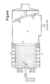
- an ion milling system is provided with a plasma chamber 1 as well as a sputtering chamber 2.
- the ion milling system is used in a process of forming a superconducting film embodying the present invention.
- the ion milling system is associated with a gas source 3 which supplies the plasma chamber 1 with argon gas, however, another gas such as, for example, xenon gas, helium gas, neon gas, krypton gas or oxygen gas is available.
- the plasma chamber 1 is accompanied with a cathode 4 and a magnet unit 5, and electrons discharged from the cathode 4 are guided by the magnetic field created by the magnet unit 5, so that the argon gas supplied to the plasma chamber 1 is ionized to produce a plasma.
- a guide electrode 6 which guides the plasma to a holder 7 in the sputtering chamber 2.
- substrates 8 and 9 respectively formed with superconductive films 10 are mounted and, for this reason, subjected to a bombardment of the plasma. With the bombardment of the plasma, the surface portion of each superconductive film 10 is etched away to expose a fresh surface thereof.
- the process sequence starts with preparation of targets of various superconductive oxides indicated in Table 1.
- Each of the targets is installed in a sputtering chamber defined in a sputtering system and faced to a substrate by a distance of about 90 millimeters.
- the substrate is formed of a single crystal magnesium oxide (MgO) and has a square surface of about 10 millimeters x about 10 millimeters.
- MgO single crystal magnesium oxide
- the substrate is heated up to about 650 degrees in centigrade, and, then, a gaseous mixture is supplied to a plasma chamber of the sputtering system.
- the gaseous mixture contains argon and oxygen mixed in a proportion of 3 : 1.
- a low pressure ambient of about 5 x 10 ⁇ 8 torr is created in the plasma chamber for producing a plasma, and the plasma bombards the target, thereby allowing the superconductive oxide to be deposited to a thickness of about 2 microns on the substrate.
- the sputtering is thus carried out at about 200 watts for about 10 hours and repeated with the targets of the various superconductive oxides.
- films of the various superconductive oxides are produced on the substrates, respectively, and a plurality of films of each superconductive oxide are divided into two groups for evaluation described hereinafter.
- the superconductive films of the first groups are mounted on the holder 7 and subjected to the ion milling in an argon ambient for about 3 hours.
- the ion milling is carried out at about 600 volts for the ionization and at about 780 mA/cm2 as the beam current density.
- the superconductive films of the second groups are subjected to a heat treatment in an oxidation ambient at about 910 degrees in centigrade for about an hour.
- Jc and Tc stand for the critical current density and the critical temperature, respectively.
- the superconductive films formed by the process according to the present invention are advantageous over the superconductive films produced in the prior-art process in the surface roughness and, accordingly, the smooth topography. Moreover, no crack takes place in the superconductive films produced by the process according to the present invention, so that the production yield are improved.
- the deposition stage may be carried out by using a physical vapor deposition.
- the superconductive film may be patterned to form an electrical wiring strip.
Landscapes
- Engineering & Computer Science (AREA)
- Manufacturing & Machinery (AREA)
- Superconductor Devices And Manufacturing Methods Thereof (AREA)
- Superconductors And Manufacturing Methods Therefor (AREA)
- Inorganic Compounds Of Heavy Metals (AREA)
- Physical Vapour Deposition (AREA)
Applications Claiming Priority (2)
| Application Number | Priority Date | Filing Date | Title |
|---|---|---|---|
| JP63056809A JPH01230275A (ja) | 1988-03-10 | 1988-03-10 | 超電導薄膜の形成法 |
| JP56809/88 | 1988-03-10 |
Publications (2)
| Publication Number | Publication Date |
|---|---|
| EP0332218A2 true EP0332218A2 (de) | 1989-09-13 |
| EP0332218A3 EP0332218A3 (de) | 1990-10-03 |
Family
ID=13037713
Family Applications (1)
| Application Number | Title | Priority Date | Filing Date |
|---|---|---|---|
| EP19890104323 Withdrawn EP0332218A3 (de) | 1988-03-10 | 1989-03-10 | Verfahren zur Herstellung einer supraleitenden Schicht |
Country Status (2)
| Country | Link |
|---|---|
| EP (1) | EP0332218A3 (de) |
| JP (1) | JPH01230275A (de) |
Cited By (5)
| Publication number | Priority date | Publication date | Assignee | Title |
|---|---|---|---|---|
| US5326747A (en) * | 1991-04-09 | 1994-07-05 | Sumitomo Electric Industries, Ltd. | Process for patterning layered thin films including a superconductor |
| EP0791968A1 (de) * | 1996-02-22 | 1997-08-27 | E.I. Du Pont De Nemours And Company | Verfahren zur Leistungsverbesserung von Hochtemperatur-supraleitenden Dünnschichten |
| WO2002095084A1 (en) * | 2001-05-22 | 2002-11-28 | Commonwealth Scientific And Industrial Research Organisation | Process and apparatus for producing crystalline thin film buffer layers and structures having biaxial texture |
| US6694412B2 (en) | 1987-12-22 | 2004-02-17 | Sun Microsystems, Inc. | Multiprocessor digital data processing system |
| AU2002302168B2 (en) * | 2001-05-22 | 2007-11-08 | Commonwealth Scientific And Industrial Research Organisation | Process and apparatus for producing crystalline thin film buffer layers and structures having biaxial texture |
Family Cites Families (1)
| Publication number | Priority date | Publication date | Assignee | Title |
|---|---|---|---|---|
| US4456506A (en) * | 1982-01-28 | 1984-06-26 | Sperry Corporation | Superconducting circuit fabrication |
-
1988
- 1988-03-10 JP JP63056809A patent/JPH01230275A/ja active Pending
-
1989
- 1989-03-10 EP EP19890104323 patent/EP0332218A3/de not_active Withdrawn
Cited By (5)
| Publication number | Priority date | Publication date | Assignee | Title |
|---|---|---|---|---|
| US6694412B2 (en) | 1987-12-22 | 2004-02-17 | Sun Microsystems, Inc. | Multiprocessor digital data processing system |
| US5326747A (en) * | 1991-04-09 | 1994-07-05 | Sumitomo Electric Industries, Ltd. | Process for patterning layered thin films including a superconductor |
| EP0791968A1 (de) * | 1996-02-22 | 1997-08-27 | E.I. Du Pont De Nemours And Company | Verfahren zur Leistungsverbesserung von Hochtemperatur-supraleitenden Dünnschichten |
| WO2002095084A1 (en) * | 2001-05-22 | 2002-11-28 | Commonwealth Scientific And Industrial Research Organisation | Process and apparatus for producing crystalline thin film buffer layers and structures having biaxial texture |
| AU2002302168B2 (en) * | 2001-05-22 | 2007-11-08 | Commonwealth Scientific And Industrial Research Organisation | Process and apparatus for producing crystalline thin film buffer layers and structures having biaxial texture |
Also Published As
| Publication number | Publication date |
|---|---|
| EP0332218A3 (de) | 1990-10-03 |
| JPH01230275A (ja) | 1989-09-13 |
Similar Documents
| Publication | Publication Date | Title |
|---|---|---|
| EP0351035A2 (de) | Herstellung von supraleitenden Oxidfilmen durch eine pre-Sauerstoff-Stickstoffglühbehandlung | |
| US4882312A (en) | Evaporation of high Tc Y-Ba-Cu-O superconducting thin film on Si and SiO2 with a zirconia buffer layer | |
| EP0337725B1 (de) | Herstellung von supraleitenden Oxidfilmen durch eine pre-Sauerstoff-Stickstoffglühbehandlung | |
| EP0292958B1 (de) | Verfahren zur Herstellung einer dünnen Schicht aus supraleitendem Mischoxid | |
| US5057201A (en) | Process for depositing a superconducting thin film | |
| EP0725448A2 (de) | Supraleitender keramischer verlängerter Gegenstand und dessen Herstellungsverfahren | |
| EP0332218A2 (de) | Verfahren zur Herstellung einer supraleitenden Schicht | |
| US4959346A (en) | Composite with Y-BA-CU-O superconductive film | |
| KR920007799B1 (ko) | 초전도 산화물 세라믹 막 제조방법 및 산화물 초전도 세라믹 막 침착장치 | |
| US6238774B1 (en) | Protection of oxide superconductor | |
| EP0526326A2 (de) | Verfahren zur Herstellung einer supraleitenden Dünnschicht aus Oxydverbindungen | |
| JPH05116940A (ja) | 基板上に金属酸化物の薄膜を生成させる方法 | |
| EP0334352B1 (de) | Supraleitender Streifen mit internem Stressabsorber | |
| EP0528332B1 (de) | Supraleitender Draht | |
| JP2713343B2 (ja) | 超電導回路の作製方法 | |
| EP0334374A2 (de) | Verfahren zur Herstellung von supraleitenden Schaltungen bei niedriger Umgebungstemperatur | |
| EP0412986B1 (de) | Epitaktische abscheidung | |
| JPH01152770A (ja) | 超電導薄膜を有する基板 | |
| JPH05213699A (ja) | 酸化物超電導体の製造方法 | |
| JP2742418B2 (ja) | 酸化物超電導薄膜の製造方法 | |
| EP0323003A2 (de) | Supraleitende Dünnschichten | |
| EP0485141B1 (de) | Verbund-Supraleiter | |
| JP2502344B2 (ja) | 複合酸化物超電導体薄膜の作製方法 | |
| EP0326087A2 (de) | Verfahren zur Herstellung einer supraleitenden Schicht | |
| JPH02141568A (ja) | 複合酸化物超電導薄膜の製造方法 |
Legal Events
| Date | Code | Title | Description |
|---|---|---|---|
| PUAI | Public reference made under article 153(3) epc to a published international application that has entered the european phase |
Free format text: ORIGINAL CODE: 0009012 |
|
| AK | Designated contracting states |
Kind code of ref document: A2 Designated state(s): DE FR GB |
|
| PUAL | Search report despatched |
Free format text: ORIGINAL CODE: 0009013 |
|
| AK | Designated contracting states |
Kind code of ref document: A3 Designated state(s): DE FR GB |
|
| 17P | Request for examination filed |
Effective date: 19910328 |
|
| RAP1 | Party data changed (applicant data changed or rights of an application transferred) |
Owner name: MITSUBISHI MATERIALS CORPORATION |
|
| 17Q | First examination report despatched |
Effective date: 19930609 |
|
| STAA | Information on the status of an ep patent application or granted ep patent |
Free format text: STATUS: THE APPLICATION HAS BEEN WITHDRAWN |
|
| 18W | Application withdrawn |
Withdrawal date: 19931209 |