EP0331498B1 - Method for providing heat resistant domain refinement of electrical steels to reduce core loss - Google Patents
Method for providing heat resistant domain refinement of electrical steels to reduce core loss Download PDFInfo
- Publication number
- EP0331498B1 EP0331498B1 EP89302104A EP89302104A EP0331498B1 EP 0331498 B1 EP0331498 B1 EP 0331498B1 EP 89302104 A EP89302104 A EP 89302104A EP 89302104 A EP89302104 A EP 89302104A EP 0331498 B1 EP0331498 B1 EP 0331498B1
- Authority
- EP
- European Patent Office
- Prior art keywords
- electron beam
- sheet
- strip
- core loss
- heat resistant
- Prior art date
- Legal status (The legal status is an assumption and is not a legal conclusion. Google has not performed a legal analysis and makes no representation as to the accuracy of the status listed.)
- Expired - Lifetime
Links
- 238000000034 method Methods 0.000 title claims abstract description 32
- 239000010959 steel Substances 0.000 title abstract description 61
- 229910000831 Steel Inorganic materials 0.000 title abstract description 60
- 238000010894 electron beam technology Methods 0.000 claims abstract description 79
- 229910000976 Electrical steel Inorganic materials 0.000 claims abstract description 26
- 230000000694 effects Effects 0.000 claims abstract description 17
- 230000007547 defect Effects 0.000 claims abstract description 13
- 238000004519 manufacturing process Methods 0.000 claims abstract description 12
- 239000011248 coating agent Substances 0.000 claims description 42
- 238000000576 coating method Methods 0.000 claims description 42
- 238000000137 annealing Methods 0.000 claims description 23
- 230000035699 permeability Effects 0.000 claims description 19
- 230000005291 magnetic effect Effects 0.000 claims description 15
- 229910052751 metal Inorganic materials 0.000 claims description 11
- 239000002184 metal Substances 0.000 claims description 11
- 238000005096 rolling process Methods 0.000 claims description 9
- 230000005381 magnetic domain Effects 0.000 claims description 6
- 238000002844 melting Methods 0.000 claims 1
- 230000008018 melting Effects 0.000 claims 1
- 238000009413 insulation Methods 0.000 abstract description 2
- 239000000696 magnetic material Substances 0.000 abstract description 2
- XUIMIQQOPSSXEZ-UHFFFAOYSA-N Silicon Chemical compound [Si] XUIMIQQOPSSXEZ-UHFFFAOYSA-N 0.000 description 12
- 229910052710 silicon Inorganic materials 0.000 description 12
- 239000010703 silicon Substances 0.000 description 12
- 239000000463 material Substances 0.000 description 9
- 239000000047 product Substances 0.000 description 9
- 239000000203 mixture Substances 0.000 description 8
- 230000009467 reduction Effects 0.000 description 7
- 229910052839 forsterite Inorganic materials 0.000 description 6
- HCWCAKKEBCNQJP-UHFFFAOYSA-N magnesium orthosilicate Chemical compound [Mg+2].[Mg+2].[O-][Si]([O-])([O-])[O-] HCWCAKKEBCNQJP-UHFFFAOYSA-N 0.000 description 6
- 238000001953 recrystallisation Methods 0.000 description 6
- 238000005097 cold rolling Methods 0.000 description 4
- 238000011161 development Methods 0.000 description 4
- 230000006872 improvement Effects 0.000 description 4
- CPLXHLVBOLITMK-UHFFFAOYSA-N magnesium oxide Inorganic materials [Mg]=O CPLXHLVBOLITMK-UHFFFAOYSA-N 0.000 description 4
- 239000000395 magnesium oxide Substances 0.000 description 4
- 239000000155 melt Substances 0.000 description 4
- 230000008569 process Effects 0.000 description 4
- 238000012545 processing Methods 0.000 description 4
- 238000007670 refining Methods 0.000 description 4
- 238000012360 testing method Methods 0.000 description 4
- 238000005266 casting Methods 0.000 description 3
- 230000001419 dependent effect Effects 0.000 description 3
- 238000009826 distribution Methods 0.000 description 3
- 230000003993 interaction Effects 0.000 description 3
- 230000007246 mechanism Effects 0.000 description 3
- 230000001681 protective effect Effects 0.000 description 3
- IJGRMHOSHXDMSA-UHFFFAOYSA-N Atomic nitrogen Chemical compound N#N IJGRMHOSHXDMSA-UHFFFAOYSA-N 0.000 description 2
- 230000006866 deterioration Effects 0.000 description 2
- 238000005530 etching Methods 0.000 description 2
- 239000011521 glass Substances 0.000 description 2
- 238000005098 hot rolling Methods 0.000 description 2
- AXZKOIWUVFPNLO-UHFFFAOYSA-N magnesium;oxygen(2-) Chemical compound [O-2].[Mg+2] AXZKOIWUVFPNLO-UHFFFAOYSA-N 0.000 description 2
- 229910052757 nitrogen Inorganic materials 0.000 description 2
- 238000010899 nucleation Methods 0.000 description 2
- 230000006911 nucleation Effects 0.000 description 2
- 239000011148 porous material Substances 0.000 description 2
- 239000000161 steel melt Substances 0.000 description 2
- 229910052717 sulfur Inorganic materials 0.000 description 2
- NINIDFKCEFEMDL-UHFFFAOYSA-N Sulfur Chemical compound [S] NINIDFKCEFEMDL-UHFFFAOYSA-N 0.000 description 1
- 238000004458 analytical method Methods 0.000 description 1
- 238000005452 bending Methods 0.000 description 1
- 230000009286 beneficial effect Effects 0.000 description 1
- 230000008901 benefit Effects 0.000 description 1
- 229910052799 carbon Inorganic materials 0.000 description 1
- 229910052802 copper Inorganic materials 0.000 description 1
- 239000010949 copper Substances 0.000 description 1
- 239000013078 crystal Substances 0.000 description 1
- 238000005520 cutting process Methods 0.000 description 1
- 125000004122 cyclic group Chemical group 0.000 description 1
- 230000007423 decrease Effects 0.000 description 1
- 238000013461 design Methods 0.000 description 1
- 230000002349 favourable effect Effects 0.000 description 1
- 239000012467 final product Substances 0.000 description 1
- 238000010438 heat treatment Methods 0.000 description 1
- 238000003384 imaging method Methods 0.000 description 1
- 239000012535 impurity Substances 0.000 description 1
- 230000006698 induction Effects 0.000 description 1
- 230000005764 inhibitory process Effects 0.000 description 1
- 230000000977 initiatory effect Effects 0.000 description 1
- SZVJSHCCFOBDDC-UHFFFAOYSA-N iron(II,III) oxide Inorganic materials O=[Fe]O[Fe]O[Fe]=O SZVJSHCCFOBDDC-UHFFFAOYSA-N 0.000 description 1
- 150000002739 metals Chemical class 0.000 description 1
- 230000004048 modification Effects 0.000 description 1
- 238000012986 modification Methods 0.000 description 1
- 150000004767 nitrides Chemical class 0.000 description 1
- 238000005457 optimization Methods 0.000 description 1
- 239000002244 precipitate Substances 0.000 description 1
- 238000000746 purification Methods 0.000 description 1
- 238000007493 shaping process Methods 0.000 description 1
- 239000011593 sulfur Substances 0.000 description 1
- 239000000725 suspension Substances 0.000 description 1
- 150000003568 thioethers Chemical class 0.000 description 1
- 238000003466 welding Methods 0.000 description 1
Images

Classifications
-
- C—CHEMISTRY; METALLURGY
- C21—METALLURGY OF IRON
- C21D—MODIFYING THE PHYSICAL STRUCTURE OF FERROUS METALS; GENERAL DEVICES FOR HEAT TREATMENT OF FERROUS OR NON-FERROUS METALS OR ALLOYS; MAKING METAL MALLEABLE, e.g. BY DECARBURISATION OR TEMPERING
- C21D1/00—General methods or devices for heat treatment, e.g. annealing, hardening, quenching or tempering
- C21D1/34—Methods of heating
-
- H—ELECTRICITY
- H01—ELECTRIC ELEMENTS
- H01F—MAGNETS; INDUCTANCES; TRANSFORMERS; SELECTION OF MATERIALS FOR THEIR MAGNETIC PROPERTIES
- H01F1/00—Magnets or magnetic bodies characterised by the magnetic materials therefor; Selection of materials for their magnetic properties
- H01F1/01—Magnets or magnetic bodies characterised by the magnetic materials therefor; Selection of materials for their magnetic properties of inorganic materials
- H01F1/03—Magnets or magnetic bodies characterised by the magnetic materials therefor; Selection of materials for their magnetic properties of inorganic materials characterised by their coercivity
- H01F1/12—Magnets or magnetic bodies characterised by the magnetic materials therefor; Selection of materials for their magnetic properties of inorganic materials characterised by their coercivity of soft-magnetic materials
- H01F1/14—Magnets or magnetic bodies characterised by the magnetic materials therefor; Selection of materials for their magnetic properties of inorganic materials characterised by their coercivity of soft-magnetic materials metals or alloys
- H01F1/16—Magnets or magnetic bodies characterised by the magnetic materials therefor; Selection of materials for their magnetic properties of inorganic materials characterised by their coercivity of soft-magnetic materials metals or alloys in the form of sheets
-
- C—CHEMISTRY; METALLURGY
- C21—METALLURGY OF IRON
- C21D—MODIFYING THE PHYSICAL STRUCTURE OF FERROUS METALS; GENERAL DEVICES FOR HEAT TREATMENT OF FERROUS OR NON-FERROUS METALS OR ALLOYS; MAKING METAL MALLEABLE, e.g. BY DECARBURISATION OR TEMPERING
- C21D8/00—Modifying the physical properties by deformation combined with, or followed by, heat treatment
- C21D8/12—Modifying the physical properties by deformation combined with, or followed by, heat treatment during manufacturing of articles with special electromagnetic properties
- C21D8/1294—Modifying the physical properties by deformation combined with, or followed by, heat treatment during manufacturing of articles with special electromagnetic properties involving a localized treatment
-
- H—ELECTRICITY
- H01—ELECTRIC ELEMENTS
- H01F—MAGNETS; INDUCTANCES; TRANSFORMERS; SELECTION OF MATERIALS FOR THEIR MAGNETIC PROPERTIES
- H01F1/00—Magnets or magnetic bodies characterised by the magnetic materials therefor; Selection of materials for their magnetic properties
- H01F1/01—Magnets or magnetic bodies characterised by the magnetic materials therefor; Selection of materials for their magnetic properties of inorganic materials
- H01F1/03—Magnets or magnetic bodies characterised by the magnetic materials therefor; Selection of materials for their magnetic properties of inorganic materials characterised by their coercivity
- H01F1/12—Magnets or magnetic bodies characterised by the magnetic materials therefor; Selection of materials for their magnetic properties of inorganic materials characterised by their coercivity of soft-magnetic materials
- H01F1/14—Magnets or magnetic bodies characterised by the magnetic materials therefor; Selection of materials for their magnetic properties of inorganic materials characterised by their coercivity of soft-magnetic materials metals or alloys
- H01F1/147—Alloys characterised by their composition
- H01F1/153—Amorphous metallic alloys, e.g. glassy metals
- H01F1/15341—Preparation processes therefor
Definitions
- This invention relates to a method for working the surface of electrical sheet or strip products to affect the domain size so as to reduce the core loss properties. More particularly, this invention relates to providing localized strains in the surface of electrical steels to provide heat resistant domain refinement.
- the Goss secondary recrystallization texture (110) [001] in terms of Miller's indices, results in improved magnetic properties, particularly permeability and core loss over nonoriented silicon steels.
- the Goss texture refers to the body-centered cubic lattice comprising the grain or crystal being oriented in the cube-on-edge position.
- the texture or grain orientation of this type has a cube edge parallel to the rolling direction and in the plane of rolling. with the (110) plane being in the sheet plane.
- steels having this orientation are characterized by a relatively high permeability in the rolling direction and a relatively low permeability in a direction at right angles thereto.
- typical steps include providing a melt having of the order of 2-4.5% silicon, casting the melt, hot rolling, cold rolling the steel to final gauge; e.g., of up to about 14 mils (0.3556mm) and typically 7 to 9 mils (0.1778 to 0.2286mm) with an intermediate annealing when two or more cold rollings are used, decarburizing the steel, applying a refractory oxide base coating, such as a magnesium oxide coating, to the steel, and final texture annealing the steel at elevated temperatures in order to produce the desired secondary recrystallization and purification treatment to remove impurities such as nitrogen and sulfur.
- the development of the cube-on-edge orientation is dependent upon the mechanism of secondary recrystallization wherein during recrystallization, secondary cube-on-edge oriented grains are preferentially grown at the expense of primary grains having a different and undesirable orientation.
- Grain-oriented silicon steel is conventionally used in electrical applications, such as power transformers, distribution transformers, generators, and the like.
- the domain structure and resistivity of the steel in electrical applications permits cyclic variation of the applied magnetic field with limited energy loss, which is termed "core loss". It is desirable, therefore, in steels used for such applications, that such steels have reduced core loss values.
- sheet and “strip” are used interchangeably and mean the same unless otherwise specified.
- first, regular or conventional grain oriented silicon steel and second, high permeability grain oriented silicon steel are generally characterized by permeabilities of less than 1850 at 10 Oersteds (795.77A/m) with a core loss of greater than 0.400 watts per pound (WPP) (0.882 watts per kilogram) at 1.5 Tesla at 60 Hertz for nominally 8 mil (0.2286mm) material.
- WPP watts per pound
- High permeability grain oriented silicon steels are characterized by higher permeabilities and lower core losses. Such higher permeability steels may be the result of compositional changes alone or together with process changes.
- high permeability silicon steels may contain nitrides, sulfides and/or borides which contribute to the precipitates and inclusions of the inhibition system which contribute to the properties of the final steel product.
- high permeability silicon steels generally undergo cold reduction operations to final gauge wherein a final heavy cold reduction of the order of greater than 80% is made in order to facilitate the grain orientation.
- domain size and thereby core loss values of electrical steels may be reduced if the steel is subjected to any of various practices to induce localized strains in the surface of the steel.
- Such practices may be generally referred to as “scribing” or “domain refining” and are performed after the final high temperature annealing operation. If the steel is scribed after the final texture annealing, then there is induced a localized stress state in the texture annealed sheet so that the domain wall spacing is reduced.
- These disturbances typically are relatively narrow, straight lines, or scribes generally spaced at regular intervals. The scribe lines are substantially transverse to the rolling direction and typically are applied to only one side of the steel.
- the particular end use and the fabrication techniques may require that the scribed steel product survive a stress relief anneal (SRA), while other products do not undergo such an SRA.
- SRA stress relief anneal
- a flat, domain refined silicon steel which is not subjected to stress relief annealing.
- the scribed steel does not have to provide heat resistant domain refinement.
- What is needed is a method and apparatus for treating electrical sheet products to effect domain refinement which is heat resistant and can withstand a stress relief anneal (SRA) typically used in the fabrication of transformers. Still further, the method and apparatus should be suitable for treating grain-oriented silicon steels of both the high permeability and conventional types as well as amorphous type electrical materials.
- SRA stress relief anneal
- a method for improving the core loss of an electrical sheet or strip having final annealed magnetic domain structures as set-out in the appended claims and which in its principal features includes subjecting at least one surface of the sheet to an electron beam treatment Lo produce narrow substantially parallel bands of treated regions separated by untreated regions substantially transverse to the direction of sheet manufacture.
- the electron beam treatment includes providing an energy density sufficient to produce a permanent defect in each treated region to effect a refinement of magnetic domain wall spacing which is heat resistant.
- the treated sheet or strip may be subsequently processed by annealing, applying a tension coating, or some combination to reduce the core loss.
- a method for improving the magnetic properties of regular and high permeability grain-oriented silicon steels and amorphous materials.
- the method is useful for treating such steels to effect a permanent refinement of the magnetic domain wall spacing for improving core loss of the steel strip.
- the width of the scribed lines and the spacing of the treated regions or lines substantially transverse to the rolling direction of the silicon strip and the casting direction of amorphous material is conventional. What is not conventional, however, is the method of the present invention for effecting such magnetic domain wall spacing in a controlled manner such that the steel so treated has improved magnetic properties which are heat resistant to survive a stress relief anneal (SRA).
- SRA stress relief anneal
- Typical electron beam generating equipment used in welding and cutting requires that the electron beam be generated in and used in at least a partial vacuum in order to provide control of the beam and spot size or width focused on the workpiece.
- Such typical equipment was modified and used in the development of the present invention.
- a particular modification included high frequency electron beam deflection coils to generate selected patterns to scan the electrical sheet.
- the speed at which the electron beam traversed the steel sheets was controlled in the laboratory development work by setting the scan frequency with a wave form generator (sold by Wavetek) which drove the electron beam deflection coils.
- the electron beam useful in the present invention could have a direct current (DC) for providing continuous beam energy or a modulated current for providing pulsed or discontinuous beam energy.
- DC direct current
- the DC electron beam was used in the examples.
- a single electron beam was used, a plurality of beams may be used to create a single treated region or to create a plurality of regions at the same time.
- the current of the electron beam may range from 0.5 to 100 milliamperes (ma); however, narrower preferred ranges may be selected for specific equipment and conditions as described herein.
- the voltage of the electron beam generated may range from 20 to 200 kilovolts (kV), preferably 60 to 150 kV. For these ranges of currents and voltages, the speed at which the electron beam traverses the steel strip must be properly selected in order to effect the domain refinement and create a permanent defect which will improve core loss values which survive subsequent annealing. It has been found that the scanning speed may range up to 10,000 ips (254m per second).
- the parameters of current, voltage, scan speed, and strip speed are interdependent for a desired scribing effect; selected and preferred ranges of the parameters are dependent upon machine design and production requirements.
- the electron beam current is adjusted to compensate for the speed of the strip and the electron beam scan speed.
- the scan speed for a given width of strip would be determined and from that the desired and suitable electrical parameters would be set to satisfactorily treat the strip in accordance with the present invention.
- the size of the electron beam focused on and imparting energy to the strip is also an important factor in determining the effect of domain refinement.
- Conventional electron beam generating equipment can produce electron beam diameters of the order of 4 to 16 mils (0.102 to 0.406mm) in a hard vacuum, usually less than 10 ⁇ 4 Torr (1,333 ⁇ 10 ⁇ Pa).
- the electron beam generally produced focuses an elliptical or circular spot size. It is expected that other shapes may be suitable.
- the focussed beam spot size effectively determines the width of the narrow irradiated or treated regions.
- the size across the focussed spot, in terms of diameter or width, of the electron beam used in the laboratory development work herein was of the order of 5 mils (0.127mm), unless otherwise specified.
- a key parameter for the electron beam treatment in accordance with the present invention is the energy being transferred to the electrical material. Particularly, it was found that it is not the beam power, but the energy density which is determinative of the extent of treatment to the sheet material.
- the energy density is a function of the electron current, voltage, scanning speed, spot size, and the number of teams used on the treated region.
- the energy density may be defined as the energy per area in units of Joules per square inch (J/in).
- the areal energy density should be about 150 J/in (23.25 J/cm) or more and may range from 150 to 4000 J/in (23.25 to 620 J/cm).
- the electron beam spot size of 5 mils (0.127mm) was constant.
- the linear energy density can be simply calculated by dividing the beam power (in J/sec. units) by the beam scanning speed (in ips units). With low beam currents of 0.5 to 10 ma, the linear energy density, expressed in such units should be about 0.75 J/in. (0.3 J/cm) or more and may range from 0.75 to 20 J/in. (0.3 to 7.9 J/cm). Broadly, the upper limit of energy density is that value at which the sheet is severely damaged or cut through.
- the specific parameters within the ranges identified depend upon the type and end use of the domain refined electrical steel. When the end use is in distribution or wound core transformers, for example, where heat resistant domain refining is needed, then the parameters will need to be selected so that the controlled working and damage to the steel will survive a subsequent stress relief anneal which is used to relieve the mechanical stresses induced in making fabricated steel articles.
- the electron beam treatment for the present invention will vary somewhat between grain-oriented silicon steels of the regular or conventional type and a high permeability steel as well as with amorphous metals. Any of these magnetic materials may have an insulative coating thereon, such as a mill glass, applied coating, for combination thereof.
- Another factor to consider in establishing the parameters for electron beam treatment is whether or not the coating on the final annealed electrical steel is damaged as a result of the treatment. Generally, it would be advantageous and desirable that the coating would not be damaged or removed in the areas of the induced stress so as to avoid any subsequent recoating process.
- An acceptable trade-off, however, to subsequent recoating steps is an electron beam treatment which provides a permanent and heat resistant domain refinement.
- the present invention described in detail hereafter has utility with grain-oriented silicon steel generally, the following typical compositions are two examples of silicon steel compositions adapted for use with the present invention and which were used in developing the present invention.
- the steel melts of the two steels initially contained the nominal compositions of: Steel C N Mn S Si Cu B Fe 1 .030 50 PPM .07 .022 3.15 .22 -- Bal. 2 .030 Less than 50PPM .038 .017 3.15 .30 10 PPM Bal.
- composition ranges are in weight percent.
- Steel 1 is a conventional grain-oriented silicon steel and Steel 2 is a high permeability grain-oriented silicon steel. Both Steels 1 and 2 were produced by casting, hot rolling, normalizing, cold rolling to final gauge with an intermediate annealing when two or more cold rolling stages were used, decarburizing, coating with MgO and final texture annealing to achieve the desired secondary recrystallization of cube-on-edge orientation. After decarburizing the steel, a refractory oxide base coating containing primarily magnesium oxide was applied before final texture annealing at elevated temperature, such annealing caused a reaction at the steel surface to create a forsterite base coating. Although the steel melts of Steels 1 and 2 initially contained the nominal compositions recited above, after final texture annealing, the C, N and S were reduced to trace levels of less than about 0.001% by weight.
- the strips were about 1.2 inches (30.5mm) wide and were passed under a stationary or fixed electron beam at 3.3 ips (83.82mm/second) and subsequently stress relied annealed, tension coated, and again stress relief annealed as indicated.
- the electron beam was generated by a machine manufactured by Leybold Heraeus.
- the machine generated a beam having a spot size of about 5 mils (0.127mm) for treating the steels in a vacuum of about 10 ⁇ 4 Torr (1.333 ⁇ 10 ⁇ 2 Pa) or better.
- the parallel bands of treated regions were about 6 millimeters apart.
- Pack 40-33A was annealed at 1475°F (800°C) to flatten the strips and exhibited watt losses which were lower than the Control values.
- the strips of Pack 40-33A were then coated with a known tension coating. The watt losses were slightly lower after tension coating than the Control Pack in the as-received condition.
- Domain imaging was conducted in a known manner with magnetite suspension and flexible permanent magnets to determine the effect on domain refinement.
- Figure 2 is a 7.5X photomicrograph which shows that the domain refinement survived the SRA and tension coating.
- the pack was reannealed twice more and watt loss properties measured each time as shown with overall improvement of 4% at 1.5T and 5% at 1.7T as compared to the Control Pack. The stability of the domain refinement and its heat resistance are demonstrated by such data.
- Figure 1 is a Scanning Electron Microscope (SEM) photomicrograph in partial cross-section of a treated zone of a strip of Pack 40-33A shown by a nital-etching.
- SEM Scanning Electron Microscope
- High energy electron beam treatment produces a cavity in the metal strip which is back filled by the melted metal strip as the electron beam moves relative to the strip.
- an interface between the metal strip and the treated zone results as shown in Figure 1. Defects such as pores or "cold-shuts" (voids due to poor adhesion of the resolidified metal to the metal strip) may be created in the subsurface.
- the metal strip has a coating thereon, such as a forsterite base-coating, mill glass, or an insulation coating for example, some of the coating material may be deposited into the cavity and melted into the zone. If the resolidified metal adheres well to the cavity wall, then the interface between the strip and the resolidified zone may disappear all, or in part, due to a subsequent high temperature anneal; however, the pores and cold-shut defects remain for the nucleation of domain wall.
- a preferred mechanism for generating heat resistant domain refinement is the interaction of tension or stress with the electron beam induced defects. Such defects and any residual stresses not relieved by annealing can be sufficient for nucleation of domain walls when tension is applied. Applying a stress coating which does not degrade upon annealing will provide "heat resistant" localized stresses introduced by the tension/defect interaction.
- Epstein Packs 40-37A, 40-34A, and 40-35A contained final texture annealed strips having a forsterite base coating thereon in the Control Pack.
- the other Epstein packs contained final texture annealed strips having a forsterite base coating and a stress or tension coating thereon in the Control Pack.
- Table II demonstrates that some samples have improved magnetic core loss properties after SRA.
- Epstein Packs 40-8 and 40-37A were subjected to electron beam treatment using the same parameters as for Pack 40-33-A of Example I. The packs seemed to respond similarly. The strips treated with 150kV were bent more severely than strips scribed with 60kV even though the linear energy densities were lower. Domain images showed that the stressed zones tended to be more localized in strips scribed with 150kV. Generally, the packs exhibited a deterioration in magnetic properties in the as-treated condition; however, they also exhibited an overall 2 to 7% watt loss reduction after one SRA.
- the data demonstrate that after electron beam treatment and SRA, the watt los properties were reduced in 18 of the 21 single strips as compared to the as-received condition up to 19% improvement at 1.5T. The watt losses were lower in 20 of 21 strips up to 15% at 1.5T in the subsequent tension coated condition.
- the second SRA demonstrated the permanence of the domain refinement induced by the electron beam and tension coating since all 21 strips exhibited lower watt losses at 1.5T when compared with the as-received condition.
- the data demonstrate that the tension/defect interaction results in heat resistant domain refinement.
- the electron beam treatment of base coated strips yielded the best watt loss reductions at 4 ma and 8.6 J/in (3.44 J/cm) linear energy density.
- the permeabilities at 10 Oersteds were reduced by about 55-94 G/o e after the second SRA when compared to the as-received condition.
- Metallographic analysis of the electron beam treated zones in cross-sections etched with nital showed that the melt zone depth and width increased with either beam current or linear energy density.
- the strips treated at 4 ma and 8.6 J/in (3.44 J/cm) exhibit the deepest and widest melt zone.
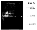
- Figure 3 is an SEM photomicrograph at 600X of Steel 2 in cross-section shown by nital etching (with copper spacer) illustrating minimal coating damage and a shallow resolidified melt zone in the treated region of about 12 microns.
- the sample of Figure 3 was subjected to electron beam treatment of 2.25 J/in. (0.9 J/cm) at 150 kV, 0.75 ma, and 50 ips (12.7 cm/sec) to affect heat resistant domain refinement just above the threshold for coating damage.
- Example IV show that the electron beam treatment was more effective on base-coated strip. Packs 2 and 3, which were stress coated prior to the electron beam treatment, did not result in reduced core loss properties under the parameters used.
- the data of Table VI show that modulated electron beam treatment produces a permanent defect to effect heat resistant domain refinement in sheet suitable to provide reduced core loss.
- Packs A and C show that base-coated material may be stress coated after electron beam treatment and thereafter subjected to an SRA and still provide reduced core loss properties in the sheet product.
- a subsequent heat treating or annealing up to 1800°F (982°C) is a critical step to achieve reductions in core loss properties. Electron beam treatment alone does not yield lower core loss properties.
- the invention includes embodiments of subsequent processing by tension coating and stress relief annealing in that order or in reversed sequence.
- a method has been developed using electron beam treatment for effecting domain refinement of electrical steels, particularly, exemplified by grain-oriented silicon steel to improve core loss values.
- a further advantage of the method of the present invention is that such improvements in core loss are heat resistant such that they survive a stress relief anneal and would be suitable for a wide variety of electrical applications.
Landscapes
- Chemical & Material Sciences (AREA)
- Engineering & Computer Science (AREA)
- Physics & Mathematics (AREA)
- Dispersion Chemistry (AREA)
- Electromagnetism (AREA)
- Power Engineering (AREA)
- Thermal Sciences (AREA)
- Mechanical Engineering (AREA)
- Materials Engineering (AREA)
- Metallurgy (AREA)
- Organic Chemistry (AREA)
- Crystallography & Structural Chemistry (AREA)
- Manufacturing & Machinery (AREA)
- Manufacturing Of Steel Electrode Plates (AREA)
- Soft Magnetic Materials (AREA)
- Manufacture Of Macromolecular Shaped Articles (AREA)
- Insulating Bodies (AREA)
- Heat Treatment Of Sheet Steel (AREA)
Abstract
Description
- This invention relates to a method for working the surface of electrical sheet or strip products to affect the domain size so as to reduce the core loss properties. More particularly, this invention relates to providing localized strains in the surface of electrical steels to provide heat resistant domain refinement.
- In the manufacture of grain oriented silicon steel, it is known that the Goss secondary recrystallization texture, (110) [001] in terms of Miller's indices, results in improved magnetic properties, particularly permeability and core loss over nonoriented silicon steels. The Goss texture refers to the body-centered cubic lattice comprising the grain or crystal being oriented in the cube-on-edge position. The texture or grain orientation of this type has a cube edge parallel to the rolling direction and in the plane of rolling. with the (110) plane being in the sheet plane. As is well known, steels having this orientation are characterized by a relatively high permeability in the rolling direction and a relatively low permeability in a direction at right angles thereto.
- In the manufacture of grain-oriented silicon steel, typical steps include providing a melt having of the order of 2-4.5% silicon, casting the melt, hot rolling, cold rolling the steel to final gauge; e.g., of up to about 14 mils (0.3556mm) and typically 7 to 9 mils (0.1778 to 0.2286mm) with an intermediate annealing when two or more cold rollings are used, decarburizing the steel, applying a refractory oxide base coating, such as a magnesium oxide coating, to the steel, and final texture annealing the steel at elevated temperatures in order to produce the desired secondary recrystallization and purification treatment to remove impurities such as nitrogen and sulfur. The development of the cube-on-edge orientation is dependent upon the mechanism of secondary recrystallization wherein during recrystallization, secondary cube-on-edge oriented grains are preferentially grown at the expense of primary grains having a different and undesirable orientation.
- Grain-oriented silicon steel is conventionally used in electrical applications, such as power transformers, distribution transformers, generators, and the like. The domain structure and resistivity of the steel in electrical applications permits cyclic variation of the applied magnetic field with limited energy loss, which is termed "core loss". It is desirable, therefore, in steels used for such applications, that such steels have reduced core loss values.
- As used herein, "sheet" and "strip" are used interchangeably and mean the same unless otherwise specified.
- It is also known that through the efforts of many prior art workers, cube-on-edge grain-oriented silicon steels generally fall into two basic categories: first, regular or conventional grain oriented silicon steel and second, high permeability grain oriented silicon steel. Regular grain oriented silicon steel is generally characterized by permeabilities of less than 1850 at 10 Oersteds (795.77A/m) with a core loss of greater than 0.400 watts per pound (WPP) (0.882 watts per kilogram) at 1.5 Tesla at 60 Hertz for nominally 8 mil (0.2286mm) material. High permeability grain oriented silicon steels are characterized by higher permeabilities and lower core losses. Such higher permeability steels may be the result of compositional changes alone or together with process changes. For example, high permeability silicon steels may contain nitrides, sulfides and/or borides which contribute to the precipitates and inclusions of the inhibition system which contribute to the properties of the final steel product. Furthermore, such high permeability silicon steels generally undergo cold reduction operations to final gauge wherein a final heavy cold reduction of the order of greater than 80% is made in order to facilitate the grain orientation.
- It is known that domain size and thereby core loss values of electrical steels, such as amorphous materials and particularly grain-oriented silicon steels, may be reduced if the steel is subjected to any of various practices to induce localized strains in the surface of the steel. Such practices may be generally referred to as "scribing" or "domain refining" and are performed after the final high temperature annealing operation. If the steel is scribed after the final texture annealing, then there is induced a localized stress state in the texture annealed sheet so that the domain wall spacing is reduced. These disturbances typically are relatively narrow, straight lines, or scribes generally spaced at regular intervals. The scribe lines are substantially transverse to the rolling direction and typically are applied to only one side of the steel.
- In the use of such amorphous and grain-oriented silicon steels, the particular end use and the fabrication techniques may require that the scribed steel product survive a stress relief anneal (SRA), while other products do not undergo such an SRA. During fabrication incident to the production of stacked core transformers and, more particularly, in the power transformers of the United States, there is a demand for a flat, domain refined silicon steel which is not subjected to stress relief annealing. In other words, the scribed steel does not have to provide heat resistant domain refinement.
- During the fabrication incident to the production of other transformers, such as most distribution transformers in the United States, the steel is cut and subjected to various bending and shaping operations which produce stresses in the steel. In such instances, it is necessary and conventional for manufacturers to stress relief anneal the product to relieve such stresses. During stress relief annealing, it has been found that the beneficial effect on core loss resulting from some scribing techniques, such as thermal scribing, are lost. For such end uses, it is required and desired that the product exhibit heat resistant domain refinement (HRDR) in order to retain the improvements in core loss values resulting from scribing.
- It has also been suggested in prior patent art that electron beam technology may be suitable for scribing silicon steel. U.S. Patent 3,990,923-Takashina et al., dated November 9, 1976 discloses that electron beams may be used on primary recrystallized silicon steel to control or inhibit the growth of secondary recrystallization grains. U.S. Patent 4,554,029-Schoen et al., dated November 19, 1985, generally discloses that electron beam resistance heating may be used on finally annealed electrical steel if damage of the insulated coating is not of concern. The damage to the insulative coating and requirements of a vacuum were considered to be major drawbacks. There is no teaching or suggestion in the art, however, of any actual or practical use of electron beam technology for scribing electrical steels.
- What is needed is a method and apparatus for treating electrical sheet products to effect domain refinement which is heat resistant and can withstand a stress relief anneal (SRA) typically used in the fabrication of transformers. Still further, the method and apparatus should be suitable for treating grain-oriented silicon steels of both the high permeability and conventional types as well as amorphous type electrical materials.
- The present invention is defined in the appended claim 1.
- Preferred embodiments are disclosed in claims 2 to 13.
- In accordance with an embodiment of the present invention, there is provided a method for improving the core loss of an electrical sheet or strip having final annealed magnetic domain structures as set-out in the appended claims and which in its principal features includes subjecting at least one surface of the sheet to an electron beam treatment Lo produce narrow substantially parallel bands of treated regions separated by untreated regions substantially transverse to the direction of sheet manufacture. The electron beam treatment includes providing an energy density sufficient to produce a permanent defect in each treated region to effect a refinement of magnetic domain wall spacing which is heat resistant. The treated sheet or strip may be subsequently processed by annealing, applying a tension coating, or some combination to reduce the core loss.
- The invention will be more particularly described in the following description and with reference to the accompanying drawings, in which:-
- Figure 1 is a photomicrograph in partial cross-section of Steel 2 of Example I showing a typical treated region.
- Figure 2 is a 7.5X photomicrograph of the magnetic domain structure of Steel 2 of Example I, in accordance with the present invention.
- Figure 3 is a photomicrograph in cross-section of Steel 2 illustrating coating damage and a resolidified melt zone.
- Broadly, in accordance with the present invention, a method is provided for improving the magnetic properties of regular and high permeability grain-oriented silicon steels and amorphous materials. Preferably, the method is useful for treating such steels to effect a permanent refinement of the magnetic domain wall spacing for improving core loss of the steel strip. The width of the scribed lines and the spacing of the treated regions or lines substantially transverse to the rolling direction of the silicon strip and the casting direction of amorphous material is conventional. What is not conventional, however, is the method of the present invention for effecting such magnetic domain wall spacing in a controlled manner such that the steel so treated has improved magnetic properties which are heat resistant to survive a stress relief anneal (SRA).
- Typical electron beam generating equipment used in welding and cutting, for example, requires that the electron beam be generated in and used in at least a partial vacuum in order to provide control of the beam and spot size or width focused on the workpiece. Such typical equipment was modified and used in the development of the present invention. A particular modification included high frequency electron beam deflection coils to generate selected patterns to scan the electrical sheet. The speed at which the electron beam traversed the steel sheets was controlled in the laboratory development work by setting the scan frequency with a wave form generator (sold by Wavetek) which drove the electron beam deflection coils.
- As used herein, the electron beam useful in the present invention could have a direct current (DC) for providing continuous beam energy or a modulated current for providing pulsed or discontinuous beam energy. Unless otherwise specified herein, the DC electron beam was used in the examples. Furthermore although a single electron beam was used, a plurality of beams may be used to create a single treated region or to create a plurality of regions at the same time.
- Other parameters or conditions of the electron beam must also be selected within certain ranges in order to provide the proper balance to effect the domain refinement. The current of the electron beam may range from 0.5 to 100 milliamperes (ma); however, narrower preferred ranges may be selected for specific equipment and conditions as described herein. The voltage of the electron beam generated may range from 20 to 200 kilovolts (kV), preferably 60 to 150 kV. For these ranges of currents and voltages, the speed at which the electron beam traverses the steel strip must be properly selected in order to effect the domain refinement and create a permanent defect which will improve core loss values which survive subsequent annealing. It has been found that the scanning speed may range up to 10,000 ips (254m per second). It should be understood that the parameters of current, voltage, scan speed, and strip speed are interdependent for a desired scribing effect; selected and preferred ranges of the parameters are dependent upon machine design and production requirements. For example, the electron beam current is adjusted to compensate for the speed of the strip and the electron beam scan speed. As a practical matter, based on the speed of the strip, the scan speed for a given width of strip would be determined and from that the desired and suitable electrical parameters would be set to satisfactorily treat the strip in accordance with the present invention.
- The size of the electron beam focused on and imparting energy to the strip is also an important factor in determining the effect of domain refinement. Conventional electron beam generating equipment can produce electron beam diameters of the order of 4 to 16 mils (0.102 to 0.406mm) in a hard vacuum, usually less than 10⁻⁴ Torr (1,333·10⁻ Pa). The electron beam generally produced focuses an elliptical or circular spot size. It is expected that other shapes may be suitable. The focussed beam spot size effectively determines the width of the narrow irradiated or treated regions. The size across the focussed spot, in terms of diameter or width, of the electron beam used in the laboratory development work herein was of the order of 5 mils (0.127mm), unless otherwise specified.
- A key parameter for the electron beam treatment in accordance with the present invention is the energy being transferred to the electrical material. Particularly, it was found that it is not the beam power, but the energy density which is determinative of the extent of treatment to the sheet material. The energy density is a function of the electron current, voltage, scanning speed, spot size, and the number of teams used on the treated region. The energy density may be defined as the energy per area in units of Joules per square inch (J/in). The areal energy density should be about 150 J/in (23.25 J/cm) or more and may range from 150 to 4000 J/in (23.25 to 620 J/cm). In developing the present invention, the electron beam spot size of 5 mils (0.127mm) was constant. The linear energy density can be simply calculated by dividing the beam power (in J/sec. units) by the beam scanning speed (in ips units). With low beam currents of 0.5 to 10 ma, the linear energy density, expressed in such units should be about 0.75 J/in. (0.3 J/cm) or more and may range from 0.75 to 20 J/in. (0.3 to 7.9 J/cm). Broadly, the upper limit of energy density is that value at which the sheet is severely damaged or cut through.
- The specific parameters within the ranges identified depend upon the type and end use of the domain refined electrical steel. When the end use is in distribution or wound core transformers, for example, where heat resistant domain refining is needed, then the parameters will need to be selected so that the controlled working and damage to the steel will survive a subsequent stress relief anneal which is used to relieve the mechanical stresses induced in making fabricated steel articles. The electron beam treatment for the present invention will vary somewhat between grain-oriented silicon steels of the regular or conventional type and a high permeability steel as well as with amorphous metals. Any of these magnetic materials may have an insulative coating thereon, such as a mill glass, applied coating, for combination thereof. Another factor to consider in establishing the parameters for electron beam treatment is whether or not the coating on the final annealed electrical steel is damaged as a result of the treatment. Generally, it would be advantageous and desirable that the coating would not be damaged or removed in the areas of the induced stress so as to avoid any subsequent recoating process. An acceptable trade-off, however, to subsequent recoating steps is an electron beam treatment which provides a permanent and heat resistant domain refinement.
- Although the present invention described in detail hereafter has utility with grain-oriented silicon steel generally, the following typical compositions are two examples of silicon steel compositions adapted for use with the present invention and which were used in developing the present invention. The steel melts of the two steels initially contained the nominal compositions of:
Steel C N Mn S Si Cu B Fe 1 .030 50 PPM .07 .022 3.15 .22 -- Bal. 2 .030 Less than 50PPM .038 .017 3.15 .30 10 PPM Bal. - Unless otherwise noted, all composition ranges are in weight percent.
- Steel 1 is a conventional grain-oriented silicon steel and Steel 2 is a high permeability grain-oriented silicon steel. Both Steels 1 and 2 were produced by casting, hot rolling, normalizing, cold rolling to final gauge with an intermediate annealing when two or more cold rolling stages were used, decarburizing, coating with MgO and final texture annealing to achieve the desired secondary recrystallization of cube-on-edge orientation. After decarburizing the steel, a refractory oxide base coating containing primarily magnesium oxide was applied before final texture annealing at elevated temperature, such annealing caused a reaction at the steel surface to create a forsterite base coating. Although the steel melts of Steels 1 and 2 initially contained the nominal compositions recited above, after final texture annealing, the C, N and S were reduced to trace levels of less than about 0.001% by weight.
- In order to better understand the present invention, the following examples are presented.
- To illustrate the several aspects of the domain refining process of the present invention, various samples of the silicon steel having a composition similar to Steel 2 were melted, cast, hot rolled, cold rolled to a final gauge of about 9-mils (0.2286mm), intermediate annealed when necessary, decarburized, and final texture annealed with an MgO annealing separator coating. The final texture annealed and base coated sample was magnetically tested before electron beam treatment to be used as a Control Pack. One surface of the steel was subjected to an electron beam treatment to produce narrow substantially parallel bands of treated regions separated by untreated regions substantially transverse to the rolling direction. For Epstein Pack 40-33a, the strips were about 1.2 inches (30.5mm) wide and were passed under a stationary or fixed electron beam at 3.3 ips (83.82mm/second) and subsequently stress relied annealed, tension coated, and again stress relief annealed as indicated.
- The electron beam was generated by a machine manufactured by Leybold Heraeus. The machine generated a beam having a spot size of about 5 mils (0.127mm) for treating the steels in a vacuum of about 10⁻⁴ Torr (1.333·10⁻2 Pa) or better. The parallel bands of treated regions were about 6 millimeters apart.
- The magnetic properties of core loss at 60 Hertz (Hz) at 1.3, 1.5 and 1.7 Tesla, permeability at 10 Oersteds (H) (795.77A/m) and at an induction of 200 Gauss (0.02T) were determined in a conventional manner for Epstein Packs. Samples were also stress relief annealed each time at 1475°F (800°C) temperature for 2 hours in a protective atmosphere.

- Domain refinement was achieved in Pack 40-33A but the electron beam conditions were of such severity that the Epstein strips were bent and deep grooves were cut through the coating on the silicon steel. The grooves were rough to the touch and would require further processing in an effort to make a satisfactory final product.
- Because of the extreme deformation and coating damage, Pack 40-33A was annealed at 1475°F (800°C) to flatten the strips and exhibited watt losses which were lower than the Control values. The strips of Pack 40-33A were then coated with a known tension coating. The watt losses were slightly lower after tension coating than the Control Pack in the as-received condition. Domain imaging was conducted in a known manner with magnetite suspension and flexible permanent magnets to determine the effect on domain refinement. Figure 2 is a 7.5X photomicrograph which shows that the domain refinement survived the SRA and tension coating. The pack was reannealed twice more and watt loss properties measured each time as shown with overall improvement of 4% at 1.5T and 5% at 1.7T as compared to the Control Pack. The stability of the domain refinement and its heat resistance are demonstrated by such data. These favorable results indicate that at least one additional processing step is necessary to yield a heat-resistant domain refined product which initially exhibits a deterioration in magnetics in the as-treated condition.
- Figure 1 is a Scanning Electron Microscope (SEM) photomicrograph in partial cross-section of a treated zone of a strip of Pack 40-33A shown by a nital-etching. Although there is no intent to be bound by theory, there is a proposed mechanism for producing heat resistant domain refinement in accordance with the present invention. High energy electron beam treatment produces a cavity in the metal strip which is back filled by the melted metal strip as the electron beam moves relative to the strip. When the melt solidifies, an interface between the metal strip and the treated zone results as shown in Figure 1. Defects such as pores or "cold-shuts" (voids due to poor adhesion of the resolidified metal to the metal strip) may be created in the subsurface. If the metal strip has a coating thereon, such as a forsterite base-coating, mill glass, or an insulation coating for example, some of the coating material may be deposited into the cavity and melted into the zone. If the resolidified metal adheres well to the cavity wall, then the interface between the strip and the resolidified zone may disappear all, or in part, due to a subsequent high temperature anneal; however, the pores and cold-shut defects remain for the nucleation of domain wall. Another embodiment suggests that a preferred mechanism for generating heat resistant domain refinement is the interaction of tension or stress with the electron beam induced defects. Such defects and any residual stresses not relieved by annealing can be sufficient for nucleation of domain walls when tension is applied. Applying a stress coating which does not degrade upon annealing will provide "heat resistant" localized stresses introduced by the tension/defect interaction.
- By way of further examples, additional tests were performed to demonstrate the heat resistant domain refined (HRDR) magnetic properties after stress relief annealing (SRA) of the samples in Table II and III obtained from various samples of nominally 9-mil (0.2286mm) silicon steel of the typical composition of Steel 2 described in Example I and subjected to a similar stress relief anneal. For Table II, Epstein Packs 40-37A, 40-34A, and 40-35A contained final texture annealed strips having a forsterite base coating thereon in the Control Pack. The other Epstein packs contained final texture annealed strips having a forsterite base coating and a stress or tension coating thereon in the Control Pack. For Table III all of the Single Sheet Panels were final texture annealed having a forsterite base coating and a stress or tension coating thereon in the Control Pack. All of the samples were electron beam treated by fixing the samples in place to a table translated in the rolling direction and deflecting the beam to scan across the strips. Some of the samples were about 1.2 inch (30.48mm) wide strips for Epstein packs and some were 4 x 22 inch (101.6 x 558.8mm) Single Sheet panels as indicated.


- Under the experimental conditions described above for stress relief annealing for given electron eam conditions to effect domain refinement, Table II demonstrates that some samples have improved magnetic core loss properties after SRA. Epstein Packs 40-8 and 40-37A were subjected to electron beam treatment using the same parameters as for Pack 40-33-A of Example I. The packs seemed to respond similarly. The strips treated with 150kV were bent more severely than strips scribed with 60kV even though the linear energy densities were lower. Domain images showed that the stressed zones tended to be more localized in strips scribed with 150kV. Generally, the packs exhibited a deterioration in magnetic properties in the as-treated condition; however, they also exhibited an overall 2 to 7% watt loss reduction after one SRA. All but Pack 40-34A was coated with a known tension coating after the first SRA. The watt losses were slightly lower after the tension coating for Packs 4-8 and 4-37A. For these Packs, a second SRA did not improve core loss but it demonstrated the permanence of the defect in providing a heat resistant domain refinement.
- Prior to the tests for Table III, preliminary tests were conducted for traversing speeds of 1000 and 2000 ips (2540 and 5080cm/sec.) over a range of electron beam currents ranging from 2 to 10 ma resulting in linear energy densities from 0.14 to 1.47 Joules/inch (0.056 to 5.88 J/cm). Comparisons confirmed that approximately 0.3 Joules/inch (0.1 J/cm) is the threshold density at 150 kV beam voltage for initiating domain refinement. None of the samples exhibited any visible disruption or disturbance of the coating and only a slight curvature or warpage of the strip. Although all of the samples exhibited significant core loss reductions in the as-treated condition, none of the samples exhibited any significant heat resistant domain refinement after SRA confirming the need for higher energy density for HRDR effect.
- Various samples of nominally 9-mil (0.2286 mm) silicon steel having the typical composition of Steel 2 were prepared as described in Example II to provide final texture annealed samples having a forsterite base coating. The samples were magnetically tested as-received to obtain control level properties. All of the samples are Epstein single strip results from strips of 1.2 x 12 inches (30.48 x 304.8mm) processed under the experimental conditions described in Table IV with parallel bands of treated regions about 6mm apart. All of the electron beam domain refining treatment was done with an electron beam having a voltage of 150 kilovolts, a current of 3 or 4 milliamperes and scan speed of 35 or 70 ips (889 or 1778 mm/sec) to provide different linear energy density levels as indicated. All the strips were initially heat flattened by stress relief annealing as in Example I, then tension coated with a known stress coating and then subjected to a second SRA at 1475°F (800°C) for 2 hours in a protective atmosphere. Magnetic properties were determined after each step as indicated.


- Under the experimental conditions described above, the data demonstrate that after electron beam treatment and SRA, the watt los properties were reduced in 18 of the 21 single strips as compared to the as-received condition up to 19% improvement at 1.5T. The watt losses were lower in 20 of 21 strips up to 15% at 1.5T in the subsequent tension coated condition. The second SRA demonstrated the permanence of the domain refinement induced by the electron beam and tension coating since all 21 strips exhibited lower watt losses at 1.5T when compared with the as-received condition. The data demonstrate that the tension/defect interaction results in heat resistant domain refinement.
- For the experimental conditions of this example, the electron beam treatment of base coated strips yielded the best watt loss reductions at 4 ma and 8.6 J/in (3.44 J/cm) linear energy density. With these parameters, the permeabilities at 10 Oersteds were reduced by about 55-94 G/oe after the second SRA when compared to the as-received condition. Metallographic analysis of the electron beam treated zones in cross-sections etched with nital showed that the melt zone depth and width increased with either beam current or linear energy density. As shown in Table V, the strips treated at 4 ma and 8.6 J/in (3.44 J/cm) exhibit the deepest and widest melt zone. It appears that the decreases in permeability and reductions in watt loss are dependent upon the size of the electron beam created defect and should be controllable through process optimization.
TABLE V Electron Beam Conditions @150 kV Treated Zone Current (ma) Speed (ips) Linear Energy Density (J/in) Depth (um) Width (um) @ surface Width (um) @ half-depth 3 70 6.4 35 298 225 4 70 8.6 72 404 300 5 35 12.8 71 359 265 - Figure 3 is an SEM photomicrograph at 600X of Steel 2 in cross-section shown by nital etching (with copper spacer) illustrating minimal coating damage and a shallow resolidified melt zone in the treated region of about 12 microns. The sample of Figure 3 was subjected to electron beam treatment of 2.25 J/in. (0.9 J/cm) at 150 kV, 0.75 ma, and 50 ips (12.7 cm/sec) to affect heat resistant domain refinement just above the threshold for coating damage.
- Additional tests were performed to effect domain refinement by a discontinuous or modulated electron beam and to explore the order or sequence of subsequent processing steps following the electron beam treatment. The beam current was modulated by a square pulse from a waveform generator. Various samples of 9-mil (0.2286 mm) steel of Steel 2 were prepared as in Example III except strips in Packs A and C were base-coated and Packs 2 and 3 were stress-coated prior to electron beam treatment. All the magnetic properties are for 20-strip Epstein Packs of 1.2 inch (30.48mm) wire strips. One surface of each strip was subjected to an electron beam treatment using a modulated beam energy of 100 Hertz pulsing at a voltage of 150 kilovolts at the currents and energy densities indicated in Table VI. After electron beam treatment, the strips of Packs A and C were tension coated with a known stress coating and then stress relief annealed as in Example I at 1475°F (800°C) for 2 hours in a protective atmosphere as indicated. Packs 2 and 3 were subjected to the same SRA after electron beam treatment. Pack 2 was also then tension coated as indicated. Magnetic properties were determined after each step as shown.
TABLE VI Pack No./Condition Permeability Core Loss @60 Hz (mWPP) @10H @200B 1.3T 1.5T 1.7T 10.7 J/inch @ 1 mA, 14 inch/sec scan speed with 100 Hz pulse A as-recd 1910 15380 310 422 591 treated 1644 1790 551 730 956 +T-coated 1912 14290 304 410 565 SRA 1910 14490 298 403 551 2 as-recd 1909 13990 312 416 553 treated 1649 2150 533 715 948 SRA 1908 12740 311 414 553 +T-coated 1897 13160 315 417 553 10.7 J/inch @ 2 mA, 28 inch/sec scan speed with 100 Hz pulse C as-recd 1933 17540 313 426 590 treated 1410 1460 806 1040 - +T-coated 1898 12500 325 439 608 SRA 1898 15880 288 399 555 3 as-recd 1905 13330 313 418 562 scr.+SRA 1832 11170 322 460 636 - A,C - scribed as-base-coated
2,3 - scribed as-stress-coated
T-coated - Tension coated
Scr + SRA - Electron beam treatment followed by SRA - Under the experimental conditions described above, it was found that the pulsed or modulated electron beam treatment yielded minimal strip curvature even at the relatively high linear energy density of 10.7 J/in. (4.28 J/cm). All of the strips from Packs A, C, 2, and 3 were flat as-treated indicating that a SRA or other heat flattening step may be eliminated after the electron beam treatment, if a subsequent operation, such as tension coating, is to be employed.
- The data of Example IV also show that the electron beam treatment was more effective on base-coated strip. Packs 2 and 3, which were stress coated prior to the electron beam treatment, did not result in reduced core loss properties under the parameters used.
- The data of Table VI show that modulated electron beam treatment produces a permanent defect to effect heat resistant domain refinement in sheet suitable to provide reduced core loss. Furthermore, Packs A and C show that base-coated material may be stress coated after electron beam treatment and thereafter subjected to an SRA and still provide reduced core loss properties in the sheet product. In accordance with the heat resistant domain refinement process of the present invention, a subsequent heat treating or annealing up to 1800°F (982°C) is a critical step to achieve reductions in core loss properties. Electron beam treatment alone does not yield lower core loss properties. Furthermore, the invention includes embodiments of subsequent processing by tension coating and stress relief annealing in that order or in reversed sequence.
- As was an object of the present invention, a method has been developed using electron beam treatment for effecting domain refinement of electrical steels, particularly, exemplified by grain-oriented silicon steel to improve core loss values. A further advantage of the method of the present invention is that such improvements in core loss are heat resistant such that they survive a stress relief anneal and would be suitable for a wide variety of electrical applications.
Claims (13)
- A method for improving the core loss properties of electrical sheet or strip products, characterised in that the method comprises:annealing an electrical metal sheet to obtain its magnetic properties ;thereafter, subjecting at least one surface of the sheet or strip to an electron beam treatment to produce narrow substantially parallel bands of treated regions separated by untreated regions substantially transverse to the direction of sheet manufacture;said treated regions resulting from melting and resolidifying of metal in those regions;the electron beam treatment including generating an electron beam 0.1 to 0.41 mm (4 to 16 mils) wide with a voltage of 20 to 200 kilovolts and deflecting the electron beam transverse to the rolling direction at a speed of.08 to 254 metres (3.3 to 10,000 inches) per second providing an energy density of from 23.25 to 620 J/cm (150 to 4000 Joules per square inch) which is sufficient to produce a permanent defect in each treated region to effect refinement of magnetic domain wall spacing of the sheet or strip heat resistant up to 982°C (1800°F) suitable to provide reduced core loss, the method further comprising annealing the sheet or strip at temperatures up to 982°C (1800°F) to provide a sheet or strip product having reduced core loss.
- A method according to claim 1, wherein the linear energy density ranges from 0.3 J/cm, (0.75 Joules per inch) or more for an electron beam spot size of about 0.127mm (4 mils) across.
- A method according to claim 1, wherein the linear energy density ranges from 0.3 to 7.9 J/cm (0.75 to 20 Joules per inch) with a current of 0.5 to 10 milliamperes.
- A method according to claims 1 or 2, wherein the electron beam is generated with a current of 0.5 to 100 milliamperes.
- A method according to any one of the preceding claims, wherein after the electron beam treatment, recoating the sheet or strip product on at least one side.
- A method according to claim 5, wherein said recoating comprises applying a tension coating to at least one surface of the treated sheet or strip to reduce core loss.
- A method according to any one of the preceding claims, wherein the electron beam treated sheet or strip is thereafter processed by applying a tension coating to reduce core loss.
- A method according to any one of the preceding claims, comprising providing continuous electron beam energy to effect said heat resistant domain refinement.
- A method according to any one of claims 1 to 7, comprising providing discontinuous electron beam energy to effect said heat resistant domain refinement.
- A method according to any one of the preceding claims, wherein the sheet or strip is conventional cubc-on-edge grain-oriented silicon steel, high permeability cube-on-edge grain-oriented silicon steel or amorphous magnetic metal.
- A method according to any one of the preceding claims, wherein the sheet or strip final gauge ranges up to about 0.3556mm (14 mils).
- A method according to any one of the preceding claims, including the step of providing at least a partial vacuum in the vicinity of the sheet or strip being subjected to the electron beam treatment.
- A method according to any one of the preceding claims except claim 4, wherein the electron beam is generated with a voltage of 150 kilovolts and current of 4,5 or 6 milliamperes and deflecting the electron beam transverse to the rolling direction at a speed of 52.8 metres (2080 inches) per second.
Applications Claiming Priority (2)
| Application Number | Priority Date | Filing Date | Title |
|---|---|---|---|
| US07/163,670 US4915750A (en) | 1988-03-03 | 1988-03-03 | Method for providing heat resistant domain refinement of electrical steels to reduce core loss |
| US163670 | 1998-09-30 |
Publications (3)
| Publication Number | Publication Date |
|---|---|
| EP0331498A2 EP0331498A2 (en) | 1989-09-06 |
| EP0331498A3 EP0331498A3 (en) | 1991-09-18 |
| EP0331498B1 true EP0331498B1 (en) | 1996-05-15 |
Family
ID=22591059
Family Applications (1)
| Application Number | Title | Priority Date | Filing Date |
|---|---|---|---|
| EP89302104A Expired - Lifetime EP0331498B1 (en) | 1988-03-03 | 1989-03-02 | Method for providing heat resistant domain refinement of electrical steels to reduce core loss |
Country Status (7)
| Country | Link |
|---|---|
| US (1) | US4915750A (en) |
| EP (1) | EP0331498B1 (en) |
| JP (1) | JPH01281709A (en) |
| KR (1) | KR960014945B1 (en) |
| AT (1) | ATE138109T1 (en) |
| BR (1) | BR8900960A (en) |
| DE (1) | DE68926470T2 (en) |
Families Citing this family (13)
| Publication number | Priority date | Publication date | Assignee | Title |
|---|---|---|---|---|
| JP3023242B2 (en) * | 1992-05-29 | 2000-03-21 | 川崎製鉄株式会社 | Method for producing low iron loss unidirectional silicon steel sheet with excellent noise characteristics |
| US5296051A (en) * | 1993-02-11 | 1994-03-22 | Kawasaki Steel Corporation | Method of producing low iron loss grain-oriented silicon steel sheet having low-noise and superior shape characteristics |
| DE19625851A1 (en) * | 1996-06-27 | 1998-01-02 | Ebetech Electron Beam Technolo | Amorphous layer crystallisation using focussed electron beam |
| JP4398666B2 (en) * | 2002-05-31 | 2010-01-13 | 新日本製鐵株式会社 | Unidirectional electrical steel sheet with excellent magnetic properties and method for producing the same |
| US8314357B2 (en) * | 2009-05-08 | 2012-11-20 | Children's Hospital And Research Center At Oakland | Joule heated nanowire biosensors |
| US20130228251A1 (en) * | 2010-08-06 | 2013-09-05 | Jfe Steel Corporation | Grain oriented electrical steel sheet and method for manufacturing the same |
| JP5870580B2 (en) * | 2011-09-26 | 2016-03-01 | Jfeスチール株式会社 | Method for producing grain-oriented electrical steel sheet |
| EP2799579B1 (en) * | 2011-12-28 | 2018-06-20 | JFE Steel Corporation | Grain-oriented electrical steel sheet and method for manufacturing the same |
| JP5594439B1 (en) * | 2012-10-31 | 2014-09-24 | Jfeスチール株式会社 | Oriented electrical steel sheet and manufacturing method thereof |
| WO2017201418A1 (en) | 2016-05-20 | 2017-11-23 | Arcanum Alloys, Inc. | Methods and systems for coating a steel substrate |
| WO2021155280A1 (en) * | 2020-01-31 | 2021-08-05 | Arcanum Alloys, Inc. | Modified steel compositions and methods related thereto |
| JP7331800B2 (en) * | 2020-07-31 | 2023-08-23 | Jfeスチール株式会社 | Oriented electrical steel sheet |
| US12030115B2 (en) | 2020-09-25 | 2024-07-09 | Metglas, Inc. | Process for in-line mechanically scribing of amorphous foil for magnetic domain alignment and core loss reduction |
Citations (1)
| Publication number | Priority date | Publication date | Assignee | Title |
|---|---|---|---|---|
| EP0108573A2 (en) * | 1982-11-08 | 1984-05-16 | Armco Inc. | Local heat treatment of electrical steel |
Family Cites Families (12)
| Publication number | Priority date | Publication date | Assignee | Title |
|---|---|---|---|---|
| DE2408878C3 (en) * | 1974-02-23 | 1979-08-16 | Kloeckner-Werke Ag, 4100 Duisburg | Device for the injection molding of moldings from unfired ceramic masses |
| JPS5423647B2 (en) * | 1974-04-25 | 1979-08-15 | ||
| GB2062972B (en) * | 1979-10-19 | 1983-08-10 | Nippon Steel Corp | Iron core for electrical machinery and apparatus and well as method for producing the iron core |
| US4645547A (en) * | 1982-10-20 | 1987-02-24 | Westinghouse Electric Corp. | Loss ferromagnetic materials and methods of improvement |
| GB8324643D0 (en) * | 1983-09-14 | 1983-10-19 | British Steel Corp | Production of grain orientated steel |
| US4655854A (en) * | 1983-10-27 | 1987-04-07 | Kawasaki Steel Corporation | Grain-oriented silicon steel sheet having a low iron loss free from deterioration due to stress-relief annealing and a method of producing the same |
| JPS60213005A (en) * | 1984-04-06 | 1985-10-25 | Mitsubishi Electric Corp | Manufacture of amorphous magnetic core |
| US4724015A (en) * | 1984-05-04 | 1988-02-09 | Nippon Steel Corporation | Method for improving the magnetic properties of Fe-based amorphous-alloy thin strip |
| GB2168626B (en) * | 1984-11-10 | 1987-12-23 | Nippon Steel Corp | Grain-oriented electrical steel sheet having stable magnetic properties resistant to stress-relief annealing, and method and apparatus for producing the same |
| JPH0672266B2 (en) * | 1987-01-28 | 1994-09-14 | 川崎製鉄株式会社 | Method for manufacturing ultra low iron loss unidirectional silicon steel sheet |
| US4909864A (en) * | 1986-09-16 | 1990-03-20 | Kawasaki Steel Corp. | Method of producing extra-low iron loss grain oriented silicon steel sheets |
| EP0875587B1 (en) * | 1997-04-30 | 2001-01-31 | Corus UK Limited | Iron or sintering process with reduced emissions of toxic gases |
-
1988
- 1988-03-03 US US07/163,670 patent/US4915750A/en not_active Expired - Fee Related
-
1989
- 1989-03-02 KR KR1019890002564A patent/KR960014945B1/en not_active IP Right Cessation
- 1989-03-02 DE DE68926470T patent/DE68926470T2/en not_active Expired - Fee Related
- 1989-03-02 AT AT89302104T patent/ATE138109T1/en not_active IP Right Cessation
- 1989-03-02 EP EP89302104A patent/EP0331498B1/en not_active Expired - Lifetime
- 1989-03-02 BR BR898900960A patent/BR8900960A/en unknown
- 1989-03-03 JP JP1051830A patent/JPH01281709A/en active Pending
Patent Citations (1)
| Publication number | Priority date | Publication date | Assignee | Title |
|---|---|---|---|---|
| EP0108573A2 (en) * | 1982-11-08 | 1984-05-16 | Armco Inc. | Local heat treatment of electrical steel |
Also Published As
| Publication number | Publication date |
|---|---|
| KR960014945B1 (en) | 1996-10-21 |
| JPH01281709A (en) | 1989-11-13 |
| EP0331498A2 (en) | 1989-09-06 |
| DE68926470T2 (en) | 1996-10-02 |
| BR8900960A (en) | 1989-10-24 |
| KR890014756A (en) | 1989-10-25 |
| DE68926470D1 (en) | 1996-06-20 |
| EP0331498A3 (en) | 1991-09-18 |
| US4915750A (en) | 1990-04-10 |
| ATE138109T1 (en) | 1996-06-15 |
Similar Documents
| Publication | Publication Date | Title |
|---|---|---|
| EP0334223B1 (en) | Ultra-rapid heat treatment of grain oriented electrical steel | |
| EP0331497B1 (en) | Method for improving core loss properties of electrical sheet product | |
| JP3023242B2 (en) | Method for producing low iron loss unidirectional silicon steel sheet with excellent noise characteristics | |
| EP0331498B1 (en) | Method for providing heat resistant domain refinement of electrical steels to reduce core loss | |
| KR20180073306A (en) | Grain oriented electrical steel sheet and method for refining magnetic domains therein | |
| KR102133909B1 (en) | Grain oriented electrical steel sheet and method for manufacturing the same | |
| US4545828A (en) | Local annealing treatment for cube-on-edge grain oriented silicon steel | |
| US20230060105A1 (en) | Grain-oriented electrical steel sheet and magnetic domain refinement method thereof | |
| KR100345723B1 (en) | Method for manufacturing a grain oriented electrical steel sheet having a low magnetostriction and manufacturing apparaturs used therein | |
| EP0367467B1 (en) | Low iron loss grain oriented silicon steel sheets and method of producing the same | |
| KR102149826B1 (en) | Grain oriented electrical steel sheet and method for manufacturing the same | |
| EP0345936B1 (en) | Method of refining magnetic domains of electrical steels | |
| US4904313A (en) | Method of producing stable magnetic domain refinement of electrical steels by metallic contaminants | |
| JPH0432517A (en) | Production of grain-oriented silicon steel sheet reduced in iron loss | |
| US4911766A (en) | Method of refining magnetic domains of electrical steels using phosphorus | |
| US5114501A (en) | Method employing skin-pass rolling to enhance the quality of phosphorous-striped silicon steel | |
| JPH05311241A (en) | Manufacture of low core loss grain-oriented silicon steel sheet and irradiation device for electron beam | |
| KR102133910B1 (en) | Grain oriented electrical steel sheet and method for manufacturing the same | |
| US5041170A (en) | Method employing skin-pass rolling to enhance the quality of phosphorus-striped silicon steel | |
| KR840000179B1 (en) | Method of a grain-oriented electromagnetic steel sheet with improved watt loss | |
| JPS61248507A (en) | Method for improvement in magnetic properties of amorphous alloy stacked core | |
| JPH04202627A (en) | Method for irradiating electron beam | |
| JPH01127621A (en) | Production of crystal grain oriented silicon steel having small amount of added boron | |
| JP2008057001A (en) | Grain-oriented electromagnetic steel sheet | |
| JPS6139395B2 (en) |
Legal Events
| Date | Code | Title | Description |
|---|---|---|---|
| PUAI | Public reference made under article 153(3) epc to a published international application that has entered the european phase |
Free format text: ORIGINAL CODE: 0009012 |
|
| AK | Designated contracting states |
Kind code of ref document: A2 Designated state(s): AT BE CH DE FR GB IT LI LU NL SE |
|
| PUAL | Search report despatched |
Free format text: ORIGINAL CODE: 0009013 |
|
| AK | Designated contracting states |
Kind code of ref document: A3 Designated state(s): AT BE CH DE FR GB IT LI LU NL SE |
|
| 17P | Request for examination filed |
Effective date: 19920203 |
|
| 17Q | First examination report despatched |
Effective date: 19921204 |
|
| GRAA | (expected) grant |
Free format text: ORIGINAL CODE: 0009210 |
|
| AK | Designated contracting states |
Kind code of ref document: B1 Designated state(s): AT BE CH DE FR GB IT LI LU NL SE |
|
| PG25 | Lapsed in a contracting state [announced via postgrant information from national office to epo] |
Ref country code: NL Free format text: LAPSE BECAUSE OF FAILURE TO SUBMIT A TRANSLATION OF THE DESCRIPTION OR TO PAY THE FEE WITHIN THE PRESCRIBED TIME-LIMIT Effective date: 19960515 Ref country code: LI Effective date: 19960515 Ref country code: CH Effective date: 19960515 Ref country code: AT Effective date: 19960515 |
|
| REF | Corresponds to: |
Ref document number: 138109 Country of ref document: AT Date of ref document: 19960615 Kind code of ref document: T |
|
| ITF | It: translation for a ep patent filed | ||
| REF | Corresponds to: |
Ref document number: 68926470 Country of ref document: DE Date of ref document: 19960620 |
|
| ET | Fr: translation filed | ||
| NLV1 | Nl: lapsed or annulled due to failure to fulfill the requirements of art. 29p and 29m of the patents act | ||
| REG | Reference to a national code |
Ref country code: CH Ref legal event code: PL |
|
| PGFP | Annual fee paid to national office [announced via postgrant information from national office to epo] |
Ref country code: SE Payment date: 19970213 Year of fee payment: 9 Ref country code: FR Payment date: 19970213 Year of fee payment: 9 |
|
| PGFP | Annual fee paid to national office [announced via postgrant information from national office to epo] |
Ref country code: DE Payment date: 19970225 Year of fee payment: 9 |
|
| PGFP | Annual fee paid to national office [announced via postgrant information from national office to epo] |
Ref country code: GB Payment date: 19970226 Year of fee payment: 9 |
|
| PGFP | Annual fee paid to national office [announced via postgrant information from national office to epo] |
Ref country code: BE Payment date: 19970317 Year of fee payment: 9 |
|
| PLBE | No opposition filed within time limit |
Free format text: ORIGINAL CODE: 0009261 |
|
| STAA | Information on the status of an ep patent application or granted ep patent |
Free format text: STATUS: NO OPPOSITION FILED WITHIN TIME LIMIT |
|
| PG25 | Lapsed in a contracting state [announced via postgrant information from national office to epo] |
Ref country code: LU Free format text: LAPSE BECAUSE OF NON-PAYMENT OF DUE FEES Effective date: 19970331 |
|
| 26N | No opposition filed | ||
| PG25 | Lapsed in a contracting state [announced via postgrant information from national office to epo] |
Ref country code: GB Free format text: LAPSE BECAUSE OF NON-PAYMENT OF DUE FEES Effective date: 19980302 |
|
| PG25 | Lapsed in a contracting state [announced via postgrant information from national office to epo] |
Ref country code: SE Free format text: LAPSE BECAUSE OF NON-PAYMENT OF DUE FEES Effective date: 19980303 |
|
| PG25 | Lapsed in a contracting state [announced via postgrant information from national office to epo] |
Ref country code: FR Free format text: THE PATENT HAS BEEN ANNULLED BY A DECISION OF A NATIONAL AUTHORITY Effective date: 19980331 Ref country code: BE Free format text: LAPSE BECAUSE OF NON-PAYMENT OF DUE FEES Effective date: 19980331 |
|
| BERE | Be: lapsed |
Owner name: ALLEGHENY LUDLUM CORP. Effective date: 19980331 |
|
| GBPC | Gb: european patent ceased through non-payment of renewal fee |
Effective date: 19980302 |
|
| PG25 | Lapsed in a contracting state [announced via postgrant information from national office to epo] |
Ref country code: DE Free format text: LAPSE BECAUSE OF NON-PAYMENT OF DUE FEES Effective date: 19981201 |
|
| EUG | Se: european patent has lapsed |
Ref document number: 89302104.8 |
|
| REG | Reference to a national code |
Ref country code: FR Ref legal event code: ST |
|
| PG25 | Lapsed in a contracting state [announced via postgrant information from national office to epo] |
Ref country code: IT Free format text: LAPSE BECAUSE OF NON-PAYMENT OF DUE FEES;WARNING: LAPSES OF ITALIAN PATENTS WITH EFFECTIVE DATE BEFORE 2007 MAY HAVE OCCURRED AT ANY TIME BEFORE 2007. THE CORRECT EFFECTIVE DATE MAY BE DIFFERENT FROM THE ONE RECORDED. Effective date: 20050302 |