EP0330355A2 - Cathode for electron tube - Google Patents
Cathode for electron tube Download PDFInfo
- Publication number
- EP0330355A2 EP0330355A2 EP89301345A EP89301345A EP0330355A2 EP 0330355 A2 EP0330355 A2 EP 0330355A2 EP 89301345 A EP89301345 A EP 89301345A EP 89301345 A EP89301345 A EP 89301345A EP 0330355 A2 EP0330355 A2 EP 0330355A2
- Authority
- EP
- European Patent Office
- Prior art keywords
- electron
- cathode
- layer
- oxide
- emissive
- Prior art date
- Legal status (The legal status is an assumption and is not a legal conclusion. Google has not performed a legal analysis and makes no representation as to the accuracy of the status listed.)
- Granted
Links
Images


Classifications
-
- H—ELECTRICITY
- H01—ELECTRIC ELEMENTS
- H01J—ELECTRIC DISCHARGE TUBES OR DISCHARGE LAMPS
- H01J29/00—Details of cathode-ray tubes or of electron-beam tubes of the types covered by group H01J31/00
- H01J29/02—Electrodes; Screens; Mounting, supporting, spacing or insulating thereof
- H01J29/04—Cathodes
-
- H—ELECTRICITY
- H01—ELECTRIC ELEMENTS
- H01J—ELECTRIC DISCHARGE TUBES OR DISCHARGE LAMPS
- H01J1/00—Details of electrodes, of magnetic control means, of screens, or of the mounting or spacing thereof, common to two or more basic types of discharge tubes or lamps
- H01J1/02—Main electrodes
- H01J1/13—Solid thermionic cathodes
- H01J1/14—Solid thermionic cathodes characterised by the material
- H01J1/142—Solid thermionic cathodes characterised by the material with alkaline-earth metal oxides, or such oxides used in conjunction with reducing agents, as an emissive material
-
- H—ELECTRICITY
- H01—ELECTRIC ELEMENTS
- H01J—ELECTRIC DISCHARGE TUBES OR DISCHARGE LAMPS
- H01J1/00—Details of electrodes, of magnetic control means, of screens, or of the mounting or spacing thereof, common to two or more basic types of discharge tubes or lamps
- H01J1/02—Main electrodes
- H01J1/13—Solid thermionic cathodes
- H01J1/14—Solid thermionic cathodes characterised by the material
Definitions
- This invention relates to cathodes for electron tubes such as cathode-ray tubes of TV sets and particularly to an improvement in electron emission characteristics of an oxide-coated cathode.
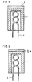
- Fig. 1 is a sectional view schematically showing a conventional oxide-coated cathode for used in a cathode-ray tube or an image pickup tube for a TV system.
- an electron-emissive substance layer 2 made of alkaline earth metal oxides containing at least Ba and further containing Sr and/or Ca is formed on a cylindrical base 1 made of Ni as a major element containing a small amount of a reducing element such as Si or Mg.
- a heater 3 is provided inside the base 1 and the electron-emissive layer 2 is heated by the heater 3 to emit thermal electrons. At this time, main donors for the emission of thermal electrons are free Ba reduced by Si, Mg or the like.
- Such a conventional cathode is manufactured by a process as described below.
- a suspension of carbonates of alkaline earth metals (Ba, Sr, Ca, etc.) is applied on the base 1 and heated in vacuum by the heater 3.
- the alkaline earth metal carbonates are converted to oxides.
- the alkaline earth metal oxides are partially reduced at a high temperature of 900 to 1100°C so that they are activated to have a semiconductive property, whereby the electron-emissive layer 2 made of alkaline earth metal oxide is formed on the base 1.
- reducing elements such as Si and Mg contained in the base 1 diffuse to move toward the interface between the alkaline earth metal oxide layer 2 and the base 1, and then react with the alkaline earth metal oxides.
- the alkaline earth metal oxide is barium oxide (BaO)
- BaO + 1/2 Si Ba + 1/2 SiO2
- BaO + Mg Ba + MgO (2)
- the alkaline earth metal oxide layer 2 formed on the base 1 is partially reduced to become a semiconductor of an oxygen deficient type. Consequently, an emission current of 0.5 to 0.8 A/cm2 is obtained under the normal condition at an operation temperature of 700 to 800°C.
- a current density higher than 0.5 to 0.8A/cm2 can not be obtained for the following reasons.
- an interface layer of oxides or composite oxides such as SiO2, MgO, and BaO.SiO2 is formed in the interface region between the base 1 and the alkaline earth metal oxide layer 2 as is obvious from the formulas (1) and (2).
- the interface layer tends to be formed at nickel crystal grain boundaries near the interface region and at a position of about 10 ⁇ m from the interface into the electron-emissive layer 2.
- This interface layer is a layer of a high resistance which obstructs flow of current.
- the interface layer prevents the reducing element in the base 1 from diffusing into the electron-emissive layer 2, and thus, prevents formation of a sufficient amount of Ba for emitting thermal electrons.
- Japanese Patent Application No. 229303/1985 discloses a cathode comprising a base 1 of Ni containing a rare earth metal of 0.1 to 0.5 wt.%.
- oxidation of the base 1 is prevented when alkaline earth metal carbonates are decomposed to form the electron-emissive layer 2 or when barium oxide is reduced during operation of the cathode.
- an interface layer of composite oxides is prevented from being formed in a concentrated manner near the interface between the base 1 and the electron-emissive layer 2, and the composite oxides is formed in a diffused manner in the electron-emissive layer 1. Accordingly, a moderate diffusion of the reducing element such as Si or Mg is maintained. As a result, there is less deterioration of the electron emission characteristics in operation of the cathode even at a high current density of about 1 to 2 A/cm2.
- Japanese Patent Application No. 160851/1985 discloses a cathode comprising an electron-emissive layer 2 containing a rare earth metal oxide of 0.1 to 20 wt.%. Also in this cathode, oxidation of the base 1 is prevented and formation of an interface layer is prevented. The electron emission characteristics of this cathode are little deteriorated in operation even at a high current density of 2A/cm2 as in the above mentioned cathode. However, a further improvement is still required. More specifically, if the cathode after the normal activation process is operated at a high current density of more than 2A/cm2, it happens that free Ba is considerably evaporated to deteriorate the electron emission characteristics.
- an object of this invention is to provide an oxide-coated cathode for an electron tube, having stable emission characteristics in operation at a current density higher than 2A/cm2.
- An oxide-coated cathode for an electron tube comprises: a base containing Ni as a major element; a reducing agent contained in the base; an electron-emissive substance layer formed on the base, containing (a) an alkaline earth metal oxide as a principal component containing at least Ba, (b) a compound of Sc, and (c) at least a heat-resisting oxide selected from the group consisting of oxides of Al, Si, Ti, V, Cr, Fe, Zr, Nb, Hf, Ta, Mo, and W; and a heater for heating the electron-emissive layer.
- An oxide-coated cathode for an electron tube comprises: a base containing Ni as a major element; a reducing agent contained in the base; a first electron-emissive layer containing (a) an alkaline earth metal oxide as a principal component containing at least Ba, and (b) a compound of Sc; a second electron-emissive layer formed on the first electron-emissive layer, containing (c) an alkaline earth metal oxide as a principal component containing at least Ba, and (d) at least one heat-resisting oxide selected from the group consisting of oxides of Al, Si, Ti, V, Cr, Fe, Zr, Nb, Hf, Ta, Mo and W; and a heater for heating the first and second electron-emissive layers.
- a cathode comprises a base 1 including Ni as a major element containing a small amount of a reducing element such as Si or Mg, and a heater 3 in the same manner as in the conventional cathodes.
- An electron-emissive layer 2 in the cathode of this embodiment contains not only triple alkaline earth metal oxides of Ba, Sr and Ca and a scandium oxide, but also at least one heat-resisting oxide selected from the group consisting of oxides of Al, Si, Ti, V, Cr, Fe, Zr, Nb, Hf, Ta, Mo and W.
- Those alkaline earth metal oxides are formed by decomposing carbonates as in the prior art and the oxides thus obtained are partially reduced and activated.
- Fig. 2 there are shown deterioration curves of electron emission characteristics of cathodes according to the embodiment.
- Those cathodes are incorporated in diode bulbs so as to be subjected to life tests at a high current density of 2.5 A/cm2 and changes in the emission current under the normal condition after the tests were examined.
- the curve A represents a deterioration of the electron emission characteristics in a cathode comprising an electron-emissive layer 2 of an alkaline earth metal oxide of Ba, Sr, and Ca containing scandium oxide (Sc2O3) of 4 wt.% and heat-resisting titanium oxide (TiO2) of 4 wt.%.
- Sc2O3 scandium oxide
- TiO2 heat-resisting titanium oxide
- the curve B represents a deterioration of the electron emission characteristics in a cathode containing heat-resisting chromium oxide (Cr2O3) of 4 wt.% in place of TiO2.
- the curve C represents a deterioration of the electron-emissive characteristics of a cathode containing Sc2O3 of 4 wt.% but not containing TiO2 nor Cr2O3
- the curve D represents a deterioration of the electron emission characteristics of a cathode not containing any of Sc2O3, TiO2 and Cr2O3.
- the cathodes containing the heat-resisting oxide Ti2O3 or Cr2O3 in addition to Sc2O3 exhibit less deterioration in the electron emission characteristics during operation at a high current density, compared with the cathodes of the prior art. It is believed that this improvement is obtained because added TiO2 or Cr2O3 prevents evaporation of free Ba as donor for thermionic emission.
- the addition amounts are preferably 0.1 to 20 wt.% for Sc2O3 and 0.5 to 10 wt.% for TiO2 and/or Cr2O3. More specifically, if the amount of Sc2O3 exceeds 20 wt.%, the initial emission current is lowered and if it is less than 0.1 wt.%, an interface layer can not be effectively prevented from being formed. If TiO2 or Cr2O3 exceeds 10 wt.%, the initial emission current is also lowered and if it is less than 0.5 wt.% conversely, evaporation of Ba can not be effectively prevented.
- Al2O3, SiO2, V2O5, Fe2O3, ZrO2, Nb2O5, HfO2, Ta2O5, MoO3 or WO3 for example may be used in place of TiO2 and/or Cr2O3.
- FIG. 3 there is shown a structure of a cathode according to another embodiment of the invention.
- the cathode of Fig. 3 is similar to that of Fig. 1, except that the electron-emissive layer 2 in Fig. 3 includes a first sub layer 2a and a second sub layer 2b.
- a first suspension is prepared by adding and mixing scandium oxide of 50 wt.% (wt.% after barium carbonate has been converted to an oxide) into a carbonate of Ba. This suspension is applied on the base 1 to a thickness of about 10 ⁇ m by using a spray.
- a second suspension is prepared by mixing TiO2 or Cr2O3 of 4 wt.% into carbonates of Ba, Sr and Ca. This second suspension is applied on the first suspension layer to a thickness of about 90 ⁇ m.
- the carbonates are decomposed in vacuum and an activation process is applied, whereby the cathode of Fig. 3 is completed.
- Fig. 4 shows the results of life test at a high current density of 2.5 A/cm2 for cathodes thus manufactured.
- the curve E represents a deterioration of the electron emission characteristics in the cathode including the first sub layer of BaO-50wt.%Sc2O3 and the second sub layer of (Ba ⁇ Sr ⁇ Ca)O-4wt.%TiO2.
- the curve F represents a deterioration of the electron emission characteristics in the cathode including the second sub layer of (Ba ⁇ Sr ⁇ Ca)O-4wt.%Cr2O3 in place of (Ba ⁇ Sr ⁇ Ca)O-4wt.%TiO2.
- the curves C and D in Fig. 4 are the same as in Fig. 2. As is clear from Fig. 4, it is understood that the cathodes as shown in Fig. 3 exhibit less deterioration in the electron emission characteristics during operation at a high current density compared with the conventional cathodes.
- the first sub layer may contain an alkaline earth metal oxide containing at least Ba, and Sc2O3 and accordingly it may further contain an oxide of Sr or Ca.
- the thickness of the first sub layer is preferably less than 50 ⁇ m and more preferably 10 to 20 ⁇ m. This is because if the first sub layer 2a has a large thickness, the distance for the reducing agents Si and/or Mg in the base 1 to migrate to the second sub layer becomes long.
- the first sub layer is sufficiently thin and a sufficient amount of free Ba is formed in the second sub layer, the initial emission current is not lowered even if Sc2O3 of more than 20 wt.% is contained in the first sub layer.
- the heat-resisting oxide in the second sub layer is contained preferably in the range from 0.05 to 10 wt.% in order to avoid lowering of the initial emission current.
- a small amount of metal powder of Ni, Co, Fe, Al, Ti, Zr, Hf, Nb, Ta, Mo, W, Mg, Re, Os, Ir, Pt, Pd, Rh, Au, V, Cr, Mn, Cu, Zn, Bi and the like may be added into the electron-emissive layers 2, 2a and 2b and then conductivity of the electron-emissive layers can be improved.
Abstract
Description
- This invention relates to cathodes for electron tubes such as cathode-ray tubes of TV sets and particularly to an improvement in electron emission characteristics of an oxide-coated cathode.
- Fig. 1 is a sectional view schematically showing a conventional oxide-coated cathode for used in a cathode-ray tube or an image pickup tube for a TV system. In the conventional oxide-coated cathode, an electron-
emissive substance layer 2 made of alkaline earth metal oxides containing at least Ba and further containing Sr and/or Ca is formed on acylindrical base 1 made of Ni as a major element containing a small amount of a reducing element such as Si or Mg. Aheater 3 is provided inside thebase 1 and the electron-emissive layer 2 is heated by theheater 3 to emit thermal electrons. At this time, main donors for the emission of thermal electrons are free Ba reduced by Si, Mg or the like. - Such a conventional cathode is manufactured by a process as described below. First, a suspension of carbonates of alkaline earth metals (Ba, Sr, Ca, etc.) is applied on the
base 1 and heated in vacuum by theheater 3. As a result, the alkaline earth metal carbonates are converted to oxides. Then, the alkaline earth metal oxides are partially reduced at a high temperature of 900 to 1100°C so that they are activated to have a semiconductive property, whereby the electron-emissive layer 2 made of alkaline earth metal oxide is formed on thebase 1. - In the above described activation process, reducing elements such as Si and Mg contained in the
base 1 diffuse to move toward the interface between the alkaline earthmetal oxide layer 2 and thebase 1, and then react with the alkaline earth metal oxides. For example, if the alkaline earth metal oxide is barium oxide (BaO), the reaction is expressed by the following formula (1) or (2).
BaO + 1/2 Si = Ba + 1/2 SiO₂ (1)
BaO + Mg = Ba + MgO (2) - Thus, the alkaline earth
metal oxide layer 2 formed on thebase 1 is partially reduced to become a semiconductor of an oxygen deficient type. Consequently, an emission current of 0.5 to 0.8 A/cm² is obtained under the normal condition at an operation temperature of 700 to 800°C. However, in the cathode thus formed, a current density higher than 0.5 to 0.8A/cm² can not be obtained for the following reasons. As a result of the partial reduction of the alkaline earth metal oxides, an interface layer of oxides or composite oxides such as SiO₂, MgO, and BaO.SiO₂ is formed in the interface region between thebase 1 and the alkaline earthmetal oxide layer 2 as is obvious from the formulas (1) and (2). Particularly, the interface layer tends to be formed at nickel crystal grain boundaries near the interface region and at a position of about 10µm from the interface into the electron-emissive layer 2. This interface layer is a layer of a high resistance which obstructs flow of current. In addition, it is believed that the interface layer prevents the reducing element in thebase 1 from diffusing into the electron-emissive layer 2, and thus, prevents formation of a sufficient amount of Ba for emitting thermal electrons. - Japanese Patent Application No. 229303/1985 discloses a cathode comprising a
base 1 of Ni containing a rare earth metal of 0.1 to 0.5 wt.%. In this cathode, oxidation of thebase 1 is prevented when alkaline earth metal carbonates are decomposed to form the electron-emissive layer 2 or when barium oxide is reduced during operation of the cathode. In addition, an interface layer of composite oxides is prevented from being formed in a concentrated manner near the interface between thebase 1 and the electron-emissive layer 2, and the composite oxides is formed in a diffused manner in the electron-emissive layer 1. Accordingly, a moderate diffusion of the reducing element such as Si or Mg is maintained. As a result, there is less deterioration of the electron emission characteristics in operation of the cathode even at a high current density of about 1 to 2 A/cm². - Japanese Patent Application No. 160851/1985 discloses a cathode comprising an electron-
emissive layer 2 containing a rare earth metal oxide of 0.1 to 20 wt.%. Also in this cathode, oxidation of thebase 1 is prevented and formation of an interface layer is prevented. The electron emission characteristics of this cathode are little deteriorated in operation even at a high current density of 2A/cm² as in the above mentioned cathode. However, a further improvement is still required. More specifically, if the cathode after the normal activation process is operated at a high current density of more than 2A/cm², it happens that free Ba is considerably evaporated to deteriorate the electron emission characteristics. - In view of the above described prior art, an object of this invention is to provide an oxide-coated cathode for an electron tube, having stable emission characteristics in operation at a current density higher than 2A/cm².
- An oxide-coated cathode for an electron tube according to an aspect of the invention comprises: a base containing Ni as a major element; a reducing agent contained in the base; an electron-emissive substance layer formed on the base, containing (a) an alkaline earth metal oxide as a principal component containing at least Ba, (b) a compound of Sc, and (c) at least a heat-resisting oxide selected from the group consisting of oxides of Aℓ, Si, Ti, V, Cr, Fe, Zr, Nb, Hf, Ta, Mo, and W; and a heater for heating the electron-emissive layer.
- An oxide-coated cathode for an electron tube according to another aspect of the invention comprises: a base containing Ni as a major element; a reducing agent contained in the base; a first electron-emissive layer containing (a) an alkaline earth metal oxide as a principal component containing at least Ba, and (b) a compound of Sc; a second electron-emissive layer formed on the first electron-emissive layer, containing (c) an alkaline earth metal oxide as a principal component containing at least Ba, and (d) at least one heat-resisting oxide selected from the group consisting of oxides of Aℓ, Si, Ti, V, Cr, Fe, Zr, Nb, Hf, Ta, Mo and W; and a heater for heating the first and second electron-emissive layers.
- The foregoing and other objects, features, aspects and advantages of the present invention will become more apparent from the following detailed description of the present invention when taken in conjunction with the accompanying drawings.
-
- Fig. 1 is a schematic sectional view illustrating a structure of an oxide-coated cathode for an electron tube.
- Fig. 2 is a graph showing relation between the life test period and the emission current in cathodes according to an embodiment of the invention.
- Fig. 3 is a schematic sectional view illustrating a structure of a cathode according to another embodiment of the invention.
- Fig. 4 is a graph showing the relation between the life test period and the emission current in cathodes having the structure of Fig. 3.
- Referring to Fig. 1, a cathode according to an embodiment of the invention comprises a
base 1 including Ni as a major element containing a small amount of a reducing element such as Si or Mg, and aheater 3 in the same manner as in the conventional cathodes. An electron-emissive layer 2 in the cathode of this embodiment contains not only triple alkaline earth metal oxides of Ba, Sr and Ca and a scandium oxide, but also at least one heat-resisting oxide selected from the group consisting of oxides of Aℓ, Si, Ti, V, Cr, Fe, Zr, Nb, Hf, Ta, Mo and W. Those alkaline earth metal oxides are formed by decomposing carbonates as in the prior art and the oxides thus obtained are partially reduced and activated. - Referring to Fig. 2 there are shown deterioration curves of electron emission characteristics of cathodes according to the embodiment. Those cathodes are incorporated in diode bulbs so as to be subjected to life tests at a high current density of 2.5 A/cm² and changes in the emission current under the normal condition after the tests were examined. The curve A represents a deterioration of the electron emission characteristics in a cathode comprising an electron-
emissive layer 2 of an alkaline earth metal oxide of Ba, Sr, and Ca containing scandium oxide (Sc₂O₃) of 4 wt.% and heat-resisting titanium oxide (TiO₂) of 4 wt.%. The curve B represents a deterioration of the electron emission characteristics in a cathode containing heat-resisting chromium oxide (Cr₂O₃) of 4 wt.% in place of TiO₂. For comparison, the curve C represents a deterioration of the electron-emissive characteristics of a cathode containing Sc₂O₃ of 4 wt.% but not containing TiO₂ nor Cr₂O₃ and the curve D represents a deterioration of the electron emission characteristics of a cathode not containing any of Sc₂O₃, TiO₂ and Cr₂O₃. As is evident from those curves, it is understood that the cathodes containing the heat-resisting oxide Ti₂O₃ or Cr₂O₃ in addition to Sc₂O₃ exhibit less deterioration in the electron emission characteristics during operation at a high current density, compared with the cathodes of the prior art. It is believed that this improvement is obtained because added TiO₂ or Cr₂O₃ prevents evaporation of free Ba as donor for thermionic emission. - As a result of observation of the surface of the electron-
emissive layer 2 containing TiO₂ or Cr₂O₃ by using the Auger spectral analysis method, it was found that a sufficient amount of Ba exists on particles of TiO₂ or Cr₂O₃. Generally, if high current flows in the electron-emissive layer 2, temperature rises due to Joule heat and an evaporated amount of Ba increases. Accordingly, the increase of the evaporated Ba results in a short life of the cathode. In other words, it is believed that the oxide TiO₃ or Cr₂O₃ absorbs Ba and prevents evaporation thereof, thus, prolonging the life of the cathode even after operation at a high current density. - As a result of conducting experiments as to amounts of addition of Sc₂O₃, TiO₂ and Cr₂O₃, it was found that the addition amounts are preferably 0.1 to 20 wt.% for Sc₂O₃ and 0.5 to 10 wt.% for TiO₂ and/or Cr₂O₃. More specifically, if the amount of Sc₂O₃ exceeds 20 wt.%, the initial emission current is lowered and if it is less than 0.1 wt.%, an interface layer can not be effectively prevented from being formed. If TiO₂ or Cr₂O₃ exceeds 10 wt.%, the initial emission current is also lowered and if it is less than 0.5 wt.% conversely, evaporation of Ba can not be effectively prevented. Aℓ₂O₃, SiO₂, V₂O₅, Fe₂O₃, ZrO₂, Nb₂O₅, HfO₂, Ta₂O₅, MoO₃ or WO₃ for example may be used in place of TiO₂ and/or Cr₂O₃.
- Referring to Fig. 3, there is shown a structure of a cathode according to another embodiment of the invention. The cathode of Fig. 3 is similar to that of Fig. 1, except that the electron-
emissive layer 2 in Fig. 3 includes afirst sub layer 2a and asecond sub layer 2b. - Those sub layers can be manufactured by the below described process. First, in order to form the
first sub layer 2a, a first suspension is prepared by adding and mixing scandium oxide of 50 wt.% (wt.% after barium carbonate has been converted to an oxide) into a carbonate of Ba. This suspension is applied on thebase 1 to a thickness of about 10µm by using a spray. Then, in order to form thesecond sub layer 2b, a second suspension is prepared by mixing TiO₂ or Cr₂O₃ of 4 wt.% into carbonates of Ba, Sr and Ca. This second suspension is applied on the first suspension layer to a thickness of about 90µm. After that, the carbonates are decomposed in vacuum and an activation process is applied, whereby the cathode of Fig. 3 is completed. - Fig. 4 shows the results of life test at a high current density of 2.5 A/cm² for cathodes thus manufactured. The curve E represents a deterioration of the electron emission characteristics in the cathode including the first sub layer of BaO-50wt.%Sc₂O₃ and the second sub layer of (Ba·Sr·Ca)O-4wt.%TiO₂. The curve F represents a deterioration of the electron emission characteristics in the cathode including the second sub layer of (Ba·Sr·Ca)O-4wt.%Cr₂O₃ in place of (Ba·Sr·Ca)O-4wt.%TiO₂. The curves C and D in Fig. 4 are the same as in Fig. 2. As is clear from Fig. 4, it is understood that the cathodes as shown in Fig. 3 exhibit less deterioration in the electron emission characteristics during operation at a high current density compared with the conventional cathodes.
- The first sub layer may contain an alkaline earth metal oxide containing at least Ba, and Sc₂O₃ and accordingly it may further contain an oxide of Sr or Ca. The thickness of the first sub layer is preferably less than 50µm and more preferably 10 to 20µm. This is because if the
first sub layer 2a has a large thickness, the distance for the reducing agents Si and/or Mg in thebase 1 to migrate to the second sub layer becomes long. In addition, since the first sub layer is sufficiently thin and a sufficient amount of free Ba is formed in the second sub layer, the initial emission current is not lowered even if Sc₂O₃ of more than 20 wt.% is contained in the first sub layer. - On the other hand, the heat-resisting oxide in the second sub layer is contained preferably in the range from 0.05 to 10 wt.% in order to avoid lowering of the initial emission current.
- In the above described embodiments, a small amount of metal powder of Ni, Co, Fe, Aℓ, Ti, Zr, Hf, Nb, Ta, Mo, W, Mg, Re, Os, Ir, Pt, Pd, Rh, Au, V, Cr, Mn, Cu, Zn, Bi and the like may be added into the electron-
emissive layers - Although the present invention has been described and illustrated in detail, it is clearly understood that the same is by way of illustration and example only and is not to be taken by way of limitation, the spirit and scope of the present invention being limited only by the terms of the appended claims.
Claims (10)
a base (1) containing Ni as a major element, said base having an external surface;
a reducing agent contained in said base (1)
a layer (2) of an electron-emissive substance formed on a part of said external surface and containing
a heater (3) for heating said layer (2) of the electron-emissive substance.
said compound of Sc is Sc₂O₃ in the range from 0.1 to 20 wt.%.
said heat-resisting oxide is contained in the range from 0.05 to 10 wt.%.
said layer of the electron-emissive substance contains a small amount of metal powder for improving conductivity.
a base (1) containing Ni as a major element, said base having an external surface;
a reducing agent contained in said base (1);
a first electron-emissive layer (2a) formed on a part of said external surface and containing
a heater (3) for heating said first and second electron-emissive layers (2a), (2b).
said first electron-emissive layer has preferably a thickness of less than 50 µm.
said first electron-emissive layer has more preferably a thickness in the range from 10 to 20µm.
said heat-resisting oxide is contained in said second electron-emissive layer in the range from 0.05 to 10 wt.%
at least either said first electron-emissive layer or said second electron-emissive layer contains a small amount of metal powder to improve conductivity.
Applications Claiming Priority (8)
| Application Number | Priority Date | Filing Date | Title |
|---|---|---|---|
| JP4031888A JPH0787070B2 (en) | 1988-02-23 | 1988-02-23 | Electron tube cathode |
| JP40318/88 | 1988-02-23 | ||
| JP4908388A JPH06105585B2 (en) | 1988-03-01 | 1988-03-01 | Electron tube cathode |
| JP49083/88 | 1988-03-01 | ||
| JP6212188A JPH0787071B2 (en) | 1988-03-15 | 1988-03-15 | Electron tube cathode |
| JP62121/88 | 1988-03-15 | ||
| JP9787388A JPH0787072B2 (en) | 1988-04-19 | 1988-04-19 | Electron tube cathode |
| JP97873/88 | 1988-04-19 |
Publications (3)
| Publication Number | Publication Date |
|---|---|
| EP0330355A2 true EP0330355A2 (en) | 1989-08-30 |
| EP0330355A3 EP0330355A3 (en) | 1990-08-22 |
| EP0330355B1 EP0330355B1 (en) | 1994-08-03 |
Family
ID=27460888
Family Applications (1)
| Application Number | Title | Priority Date | Filing Date |
|---|---|---|---|
| EP89301345A Expired - Lifetime EP0330355B1 (en) | 1988-02-23 | 1989-02-13 | Cathode for electron tube |
Country Status (5)
| Country | Link |
|---|---|
| US (1) | US4924137A (en) |
| EP (1) | EP0330355B1 (en) |
| KR (1) | KR910009660B1 (en) |
| CA (1) | CA1327145C (en) |
| DE (1) | DE68917174T2 (en) |
Cited By (8)
| Publication number | Priority date | Publication date | Assignee | Title |
|---|---|---|---|---|
| FR2656954A1 (en) * | 1989-11-02 | 1991-07-12 | Samsung Electronic Devices | CATHODE FOR ELECTRONIC TUBE AND METHOD FOR MANUFACTURING THE SAME |
| EP0841676A1 (en) * | 1996-11-12 | 1998-05-13 | Matsushita Electronics Corporation | Cathode for electron tube and method for manufacturing the same |
| NL1004830C2 (en) * | 1995-12-27 | 1998-05-14 | Mitsubishi Electric Corp | Cathode for electron tube. |
| EP0845797A2 (en) * | 1996-11-29 | 1998-06-03 | Mitsubishi Denki Kabushiki Kaisha | Electron tube cathode |
| EP0847071A1 (en) * | 1996-02-29 | 1998-06-10 | Matsushita Electronics Corporation | Electron-tube cathode |
| GB2294155B (en) * | 1994-10-12 | 1999-03-03 | Samsung Display Devices Co Ltd | Cathode for electron tube |
| KR19990043956A (en) * | 1997-11-30 | 1999-06-25 | 김영남 | Electrode Material for CRT |
| US6033280A (en) * | 1995-09-21 | 2000-03-07 | Matsushita Electronics Corporation | Method for manufacturing emitter for cathode ray tube |
Families Citing this family (21)
| Publication number | Priority date | Publication date | Assignee | Title |
|---|---|---|---|---|
| NL8803047A (en) * | 1988-12-13 | 1990-07-02 | Philips Nv | OXIDE CATHODE. |
| KR940011717B1 (en) * | 1990-10-05 | 1994-12-23 | 가부시기가이샤 히다찌세이사구쇼 | Cathode for electron tube |
| US5828164A (en) * | 1992-04-03 | 1998-10-27 | The United States Of America As Represented By The Secretary Of The Army | Thermionic cathode using oxygen deficient and fully oxidized material for high electron density emissions |
| US5298830A (en) * | 1992-04-03 | 1994-03-29 | The United States Of America As Represented By The Secretary Of The Army | Method of preparing an impregnated cathode with an enhanced thermionic emission from a porous billet and cathode so prepared |
| KR100291903B1 (en) * | 1993-08-23 | 2001-09-17 | 김순택 | Oxide cathode of cathode ray tube |
| US5841219A (en) * | 1993-09-22 | 1998-11-24 | University Of Utah Research Foundation | Microminiature thermionic vacuum tube |
| KR960025915A (en) * | 1994-12-28 | 1996-07-20 | 윤종용 | Hot electron-emitting oxide cathode and method of manufacturing same |
| US5545945A (en) * | 1995-03-29 | 1996-08-13 | The United States Of America As Represented By The Secretary Of The Army | Thermionic cathode |
| US5955828A (en) * | 1996-10-16 | 1999-09-21 | University Of Utah Research Foundation | Thermionic optical emission device |
| KR100259420B1 (en) * | 1996-10-25 | 2000-06-15 | 구자홍 | Electron emission material compounds of electrode for crt |
| KR100249714B1 (en) * | 1997-12-30 | 2000-03-15 | 손욱 | Cathode used in an electron gun |
| US6118215A (en) * | 1998-08-07 | 2000-09-12 | Omnion Technologies, Inc. | Flat internal electrode for luminous gas discharge display and method of manufacture |
| JP2000357464A (en) * | 1999-06-14 | 2000-12-26 | Hitachi Ltd | Cathode-ray tube |
| US6362563B1 (en) * | 1999-10-05 | 2002-03-26 | Chunghwa Picture Tubes, Ltd. | Two-layer cathode for electron gun |
| FR2808377A1 (en) * | 2000-04-26 | 2001-11-02 | Thomson Tubes & Displays | OXIDE CATHODE FOR CATHODE RAY TUBE |
| JP2001345041A (en) * | 2000-06-01 | 2001-12-14 | Mitsubishi Electric Corp | Cathode for electron tube |
| FR2810446A1 (en) * | 2000-06-14 | 2001-12-21 | Thomson Tubes & Displays | Improved oxide coated cathode incorporating electrical conducting grains acting as conducting bridges between the metal support and the oxide layer through the interface layer formed between them |
| DE10121442B4 (en) * | 2000-09-19 | 2010-04-08 | Philips Intellectual Property & Standards Gmbh | Cathode ray tube with oxide cathode |
| EP1232511B1 (en) * | 2000-09-19 | 2007-08-15 | Koninklijke Philips Electronics N.V. | Oxide cathode |
| US6995502B2 (en) | 2002-02-04 | 2006-02-07 | Innosys, Inc. | Solid state vacuum devices and method for making the same |
| US7005783B2 (en) | 2002-02-04 | 2006-02-28 | Innosys, Inc. | Solid state vacuum devices and method for making the same |
Citations (7)
| Publication number | Priority date | Publication date | Assignee | Title |
|---|---|---|---|---|
| DE1120605B (en) * | 1960-09-21 | 1961-12-28 | Siemens Ag | Oxide cathode |
| US3760218A (en) * | 1972-04-10 | 1973-09-18 | Spectramat Inc | Thermionic cathode |
| JPS54142965A (en) * | 1978-04-28 | 1979-11-07 | Hitachi Ltd | Direct-heated cathode |
| JPS5574030A (en) * | 1978-11-29 | 1980-06-04 | Hitachi Ltd | Electronic tube cathode |
| JPS5730235A (en) * | 1980-07-30 | 1982-02-18 | Hitachi Ltd | Directly-heated cathode for electron tube |
| JPS6032232A (en) * | 1983-08-03 | 1985-02-19 | Hitachi Ltd | Impregnated cathode |
| EP0210805A2 (en) * | 1985-07-19 | 1987-02-04 | Mitsubishi Denki Kabushiki Kaisha | Cathode for electron tube |
Family Cites Families (4)
| Publication number | Priority date | Publication date | Assignee | Title |
|---|---|---|---|---|
| US3719856A (en) * | 1971-05-19 | 1973-03-06 | O Koppius | Impregnants for dispenser cathodes |
| NL7905542A (en) * | 1979-07-17 | 1981-01-20 | Philips Nv | DELIVERY CATHOD. |
| JPS60160851A (en) * | 1984-01-31 | 1985-08-22 | Akio Sato | Method and tool for cooking in vacuum |
| JPS60229303A (en) * | 1984-04-27 | 1985-11-14 | セイコーエプソン株式会社 | Nonlinear resistance element |
-
1988
- 1988-12-19 KR KR1019880016941A patent/KR910009660B1/en not_active IP Right Cessation
-
1989
- 1989-02-08 US US07/307,709 patent/US4924137A/en not_active Expired - Lifetime
- 1989-02-13 EP EP89301345A patent/EP0330355B1/en not_active Expired - Lifetime
- 1989-02-13 DE DE68917174T patent/DE68917174T2/en not_active Expired - Fee Related
- 1989-02-21 CA CA000591597A patent/CA1327145C/en not_active Expired - Fee Related
Patent Citations (7)
| Publication number | Priority date | Publication date | Assignee | Title |
|---|---|---|---|---|
| DE1120605B (en) * | 1960-09-21 | 1961-12-28 | Siemens Ag | Oxide cathode |
| US3760218A (en) * | 1972-04-10 | 1973-09-18 | Spectramat Inc | Thermionic cathode |
| JPS54142965A (en) * | 1978-04-28 | 1979-11-07 | Hitachi Ltd | Direct-heated cathode |
| JPS5574030A (en) * | 1978-11-29 | 1980-06-04 | Hitachi Ltd | Electronic tube cathode |
| JPS5730235A (en) * | 1980-07-30 | 1982-02-18 | Hitachi Ltd | Directly-heated cathode for electron tube |
| JPS6032232A (en) * | 1983-08-03 | 1985-02-19 | Hitachi Ltd | Impregnated cathode |
| EP0210805A2 (en) * | 1985-07-19 | 1987-02-04 | Mitsubishi Denki Kabushiki Kaisha | Cathode for electron tube |
Non-Patent Citations (4)
| Title |
|---|
| PATENT ABSTRACTS OF JAPAN vol. 4, no. 1 (E-163) 08 January 1980, & JP-A-54 142 965 (HITACHI SEISAKUSHO K. K.) 11 July 1979, * |
| PATENT ABSTRACTS OF JAPAN vol. 4, no. 117 (E-22)(599) 20 August 1980, & JP-A-55 074 030 (HITACHI SEISAKUSHO K. K.) 04 June 1980, * |
| PATENT ABSTRACTS OF JAPAN vol. 6, no. 95 (E-110)(973) 03 June 1982, & JP-A-57 030 235 (HITACHI SEISAKUSHO K. K.) 18 February 1982 * |
| PATENT ABSTRACTS OF JAPAN vol. 9, no. 150 (E-324)(1873) 25 June 1985, & JP-A-60 032 232 (HITACHI SEISAKUSHO K. K.) 19 February 1985, * |
Cited By (17)
| Publication number | Priority date | Publication date | Assignee | Title |
|---|---|---|---|---|
| FR2656954A1 (en) * | 1989-11-02 | 1991-07-12 | Samsung Electronic Devices | CATHODE FOR ELECTRONIC TUBE AND METHOD FOR MANUFACTURING THE SAME |
| GB2294155B (en) * | 1994-10-12 | 1999-03-03 | Samsung Display Devices Co Ltd | Cathode for electron tube |
| US6222308B1 (en) | 1995-09-21 | 2001-04-24 | Matsushita Electronics Corporation | Emitter material for cathode ray tube having at least one alkaline earth metal carbonate dispersed or concentrated in a mixed crystal or solid solution |
| US6033280A (en) * | 1995-09-21 | 2000-03-07 | Matsushita Electronics Corporation | Method for manufacturing emitter for cathode ray tube |
| CN1090802C (en) * | 1995-12-27 | 2002-09-11 | 三菱电机株式会社 | Cathode for electron tube |
| NL1004830C2 (en) * | 1995-12-27 | 1998-05-14 | Mitsubishi Electric Corp | Cathode for electron tube. |
| US6091189A (en) * | 1995-12-27 | 2000-07-18 | Mitsubishi Denki Kabushiki Kaisha | Cathode for an electron tube |
| EP0847071A4 (en) * | 1996-02-29 | 2000-03-01 | Matsushita Electronics Corp | Electron-tube cathode |
| EP0847071A1 (en) * | 1996-02-29 | 1998-06-10 | Matsushita Electronics Corporation | Electron-tube cathode |
| US5925976A (en) * | 1996-11-12 | 1999-07-20 | Matsushita Electronics Corporation | Cathode for electron tube having specific emissive material |
| KR100319227B1 (en) * | 1996-11-12 | 2002-02-19 | 모리시타 요이찌 | cathode for electron tube and methods for the same |
| EP0841676A1 (en) * | 1996-11-12 | 1998-05-13 | Matsushita Electronics Corporation | Cathode for electron tube and method for manufacturing the same |
| CN1123031C (en) * | 1996-11-12 | 2003-10-01 | 松下电器产业株式会社 | Valve cathode and its making method |
| EP0845797A3 (en) * | 1996-11-29 | 1999-02-17 | Mitsubishi Denki Kabushiki Kaisha | Electron tube cathode |
| US6124666A (en) * | 1996-11-29 | 2000-09-26 | Mitsubishi Denki Kabushiki Kaisha | Electron tube cathode |
| EP0845797A2 (en) * | 1996-11-29 | 1998-06-03 | Mitsubishi Denki Kabushiki Kaisha | Electron tube cathode |
| KR19990043956A (en) * | 1997-11-30 | 1999-06-25 | 김영남 | Electrode Material for CRT |
Also Published As
| Publication number | Publication date |
|---|---|
| DE68917174D1 (en) | 1994-09-08 |
| US4924137A (en) | 1990-05-08 |
| KR910009660B1 (en) | 1991-11-25 |
| EP0330355B1 (en) | 1994-08-03 |
| KR890013695A (en) | 1989-09-25 |
| EP0330355A3 (en) | 1990-08-22 |
| CA1327145C (en) | 1994-02-22 |
| DE68917174T2 (en) | 1995-01-05 |
Similar Documents
| Publication | Publication Date | Title |
|---|---|---|
| EP0330355B1 (en) | Cathode for electron tube | |
| US4797593A (en) | Cathode for electron tube | |
| JPS645417B2 (en) | ||
| US4274030A (en) | Thermionic cathode | |
| US4291252A (en) | Electron tube cathode | |
| US5548184A (en) | Oxide cathode employing Ba evaporation restraining layer | |
| US5747921A (en) | Impregnation type cathode for a cathodic ray tube | |
| JPH06101299B2 (en) | Method for manufacturing impregnated cathode | |
| KR900003175B1 (en) | Cathode in cathode ray tube | |
| JPS6288239A (en) | Cathode for electron tube | |
| JPH02288043A (en) | Cathode for electron tube | |
| EP0639848A1 (en) | Oxide cathode for electron tube | |
| DE60305931T2 (en) | OXIDE CATHODE FOR AN ELECTRON CANNON WITH A DIFFERENTLY DOTED METALLIC SUBSTRATE | |
| JPH01213932A (en) | Cathode of electron tube | |
| JPS63314741A (en) | Cathode for electron tube | |
| JPH0787072B2 (en) | Electron tube cathode | |
| JPH01315926A (en) | Cathode for electron tube | |
| JP2718389B2 (en) | Cathode for electron tube | |
| JPH0743995B2 (en) | Electron tube cathode | |
| JPS6290819A (en) | Cathode for electron tube | |
| KR920003186B1 (en) | Manufacturing method of oxide cathode | |
| JPS62165833A (en) | Cathode for electron tube | |
| JPH01213933A (en) | Cathode of electron tube | |
| JPH0546652B2 (en) | ||
| JPH0787071B2 (en) | Electron tube cathode |
Legal Events
| Date | Code | Title | Description |
|---|---|---|---|
| PUAI | Public reference made under article 153(3) epc to a published international application that has entered the european phase |
Free format text: ORIGINAL CODE: 0009012 |
|
| AK | Designated contracting states |
Kind code of ref document: A2 Designated state(s): DE FR GB NL |
|
| PUAL | Search report despatched |
Free format text: ORIGINAL CODE: 0009013 |
|
| AK | Designated contracting states |
Kind code of ref document: A3 Designated state(s): DE FR GB NL |
|
| 17P | Request for examination filed |
Effective date: 19901008 |
|
| 17Q | First examination report despatched |
Effective date: 19930128 |
|
| GRAA | (expected) grant |
Free format text: ORIGINAL CODE: 0009210 |
|
| AK | Designated contracting states |
Kind code of ref document: B1 Designated state(s): DE FR GB NL |
|
| REF | Corresponds to: |
Ref document number: 68917174 Country of ref document: DE Date of ref document: 19940908 |
|
| ET | Fr: translation filed | ||
| PLBE | No opposition filed within time limit |
Free format text: ORIGINAL CODE: 0009261 |
|
| STAA | Information on the status of an ep patent application or granted ep patent |
Free format text: STATUS: NO OPPOSITION FILED WITHIN TIME LIMIT |
|
| 26N | No opposition filed | ||
| REG | Reference to a national code |
Ref country code: GB Ref legal event code: 746 Effective date: 19971202 |
|
| REG | Reference to a national code |
Ref country code: FR Ref legal event code: D6 |
|
| REG | Reference to a national code |
Ref country code: GB Ref legal event code: IF02 |
|
| PGFP | Annual fee paid to national office [announced via postgrant information from national office to epo] |
Ref country code: FR Payment date: 20060220 Year of fee payment: 18 |
|
| PGFP | Annual fee paid to national office [announced via postgrant information from national office to epo] |
Ref country code: GB Payment date: 20070104 Year of fee payment: 19 |
|
| PGFP | Annual fee paid to national office [announced via postgrant information from national office to epo] |
Ref country code: NL Payment date: 20070215 Year of fee payment: 19 |
|
| PGFP | Annual fee paid to national office [announced via postgrant information from national office to epo] |
Ref country code: DE Payment date: 20070220 Year of fee payment: 19 |
|
| REG | Reference to a national code |
Ref country code: FR Ref legal event code: ST Effective date: 20071030 |
|
| PG25 | Lapsed in a contracting state [announced via postgrant information from national office to epo] |
Ref country code: FR Free format text: LAPSE BECAUSE OF NON-PAYMENT OF DUE FEES Effective date: 20070228 |
|
| GBPC | Gb: european patent ceased through non-payment of renewal fee |
Effective date: 20080213 |
|
| NLV4 | Nl: lapsed or anulled due to non-payment of the annual fee |
Effective date: 20080901 |
|
| PG25 | Lapsed in a contracting state [announced via postgrant information from national office to epo] |
Ref country code: NL Free format text: LAPSE BECAUSE OF NON-PAYMENT OF DUE FEES Effective date: 20080901 |
|
| PG25 | Lapsed in a contracting state [announced via postgrant information from national office to epo] |
Ref country code: DE Free format text: LAPSE BECAUSE OF NON-PAYMENT OF DUE FEES Effective date: 20080902 |
|
| PG25 | Lapsed in a contracting state [announced via postgrant information from national office to epo] |
Ref country code: GB Free format text: LAPSE BECAUSE OF NON-PAYMENT OF DUE FEES Effective date: 20080213 |