EP0328841A2 - Asymmetrischer Verzögerungsgenerator für einen Taktzerhacker - Google Patents
Asymmetrischer Verzögerungsgenerator für einen Taktzerhacker Download PDFInfo
- Publication number
- EP0328841A2 EP0328841A2 EP88480089A EP88480089A EP0328841A2 EP 0328841 A2 EP0328841 A2 EP 0328841A2 EP 88480089 A EP88480089 A EP 88480089A EP 88480089 A EP88480089 A EP 88480089A EP 0328841 A2 EP0328841 A2 EP 0328841A2
- Authority
- EP
- European Patent Office
- Prior art keywords
- transistor
- coupled
- base
- collector
- delay generator
- Prior art date
- Legal status (The legal status is an assumption and is not a legal conclusion. Google has not performed a legal analysis and makes no representation as to the accuracy of the status listed.)
- Granted
Links
Images
Classifications
-
- G—PHYSICS
- G06—COMPUTING OR CALCULATING; COUNTING
- G06F—ELECTRIC DIGITAL DATA PROCESSING
- G06F1/00—Details not covered by groups G06F3/00 - G06F13/00 and G06F21/00
- G06F1/04—Generating or distributing clock signals or signals derived directly therefrom
- G06F1/10—Distribution of clock signals, e.g. skew
-
- G—PHYSICS
- G06—COMPUTING OR CALCULATING; COUNTING
- G06F—ELECTRIC DIGITAL DATA PROCESSING
- G06F1/00—Details not covered by groups G06F3/00 - G06F13/00 and G06F21/00
- G06F1/04—Generating or distributing clock signals or signals derived directly therefrom
- G06F1/08—Clock generators with changeable or programmable clock frequency
-
- H—ELECTRICITY
- H03—ELECTRONIC CIRCUITRY
- H03K—PULSE TECHNIQUE
- H03K3/00—Circuits for generating electric pulses; Monostable, bistable or multistable circuits
- H03K3/02—Generators characterised by the type of circuit or by the means used for producing pulses
- H03K3/26—Generators characterised by the type of circuit or by the means used for producing pulses by the use, as active elements, of bipolar transistors with internal or external positive feedback
- H03K3/28—Generators characterised by the type of circuit or by the means used for producing pulses by the use, as active elements, of bipolar transistors with internal or external positive feedback using means other than a transformer for feedback
- H03K3/281—Generators characterised by the type of circuit or by the means used for producing pulses by the use, as active elements, of bipolar transistors with internal or external positive feedback using means other than a transformer for feedback using at least two transistors so coupled that the input of one is derived from the output of another, e.g. multivibrator
- H03K3/286—Generators characterised by the type of circuit or by the means used for producing pulses by the use, as active elements, of bipolar transistors with internal or external positive feedback using means other than a transformer for feedback using at least two transistors so coupled that the input of one is derived from the output of another, e.g. multivibrator bistable
- H03K3/288—Generators characterised by the type of circuit or by the means used for producing pulses by the use, as active elements, of bipolar transistors with internal or external positive feedback using means other than a transformer for feedback using at least two transistors so coupled that the input of one is derived from the output of another, e.g. multivibrator bistable using additional transistors in the input circuit
-
- H—ELECTRICITY
- H03—ELECTRONIC CIRCUITRY
- H03K—PULSE TECHNIQUE
- H03K5/00—Manipulating of pulses not covered by one of the other main groups of this subclass
- H03K5/01—Shaping pulses
- H03K5/04—Shaping pulses by increasing duration; by decreasing duration
-
- H—ELECTRICITY
- H03—ELECTRONIC CIRCUITRY
- H03K—PULSE TECHNIQUE
- H03K5/00—Manipulating of pulses not covered by one of the other main groups of this subclass
- H03K5/13—Arrangements having a single output and transforming input signals into pulses delivered at desired time intervals
Definitions
- the present invention relates to a digital logic timing circuit and particularly to a clock chopper circuit.
- master clock signals are frequently generated by a common clock generator circuit.
- the clock pulses produced thereby are distributed throughout the logic system. These clock pulses provide timing signals at a particular time within the repetitive clock cycle provided by a master system clock.
- the clock pulses may not be suitable for the purpose of controlling the operation of the circuits on a given chip.
- a clock chopper may be required on the chip to produce from the system clock pulses input thereto, a suitable set of on chip clock pulses.
- Clock chopper circuits are quite widely used in various applications. Generally, these circuits produce a pulse which has a shorter duration than the system clock pulses input thereto.
- An example of such a clock chopper is found in the IBM Technical Disclosure Bulletin, Vol. 29, No. 7, Dec. 1986. pp. 3148-3151.
- the circuit there described includes a receiver circuit coupled to the system clock for generating dual phase output clock signals.
- the dual phase output signals couple to the input of a delay generator which is configured from a complementary transistor switch (CTS) memory cell. The time required to write this cell determines the width of the generated pulse.
- the delay generator is coupled via a level converter circuit to a gate receiver circuit.
- the gate receiver is also coupled to the system clock input and has a low level output so long as both inputs thereto are at a low level.
- That clock chopper circuit has at least two unique characteristics.
- the delay generator contributes about 60% to 70% of the total pulse width formed.
- the select and reset time are nearly identical because the memory cell therein runs symmetrically.
- the cycle time for the circuit is limited to being greater than the turn on (select) and turn off (reset) time for the cell, the turn on and turn off times being approximately equal. Accordingly, circuits of the type described above are limited to applications where the cycle time is at least as long as the set and reset time of the CTS cell. The circuit simply cannot function faster.
- the present invention is generally configured as the clock chopper described in the above mentioned IBM Technical Disclosure Bulletin.
- the delay generator is constructed in a different manner.
- the CTS memory cell is configured to be asymmetrical in operation. That is the half of the cell which determines the turn on is operated in saturated mode while the other half which controls the turn off/recovery time is operated in non-saturated mode. This permits the circuit to turn off quicker and to be ready for the next system clock cycle to begin.
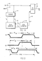
- Fig. 1A comprises a block diagram of the clock chopper circuit shown in the IBM Technical Disclosure Bulletin, Vol. 29, No. 7, Dec. 1986, pages 3148-3151. The content of that publication is incorporated herein by reference.
- the circuit has a clock input terminal 10 for receiving from an external source a clock signal which, in typical applications, comprises a substantially symmetrical square wave signal at a particular frequency.
- the circuit also includes an enable input terminal 12 for receiving a signal from the external circuitry to either enable or disenable the receiver 14 and other circuitry coupled thereto.
- the enable signal at the input terminal 12 is at its enabling state, the receiver 14 is actuated along with the other circuitry coupled thereto to ultimately produce a delayed signal on the line 16 which is input to the OR gate 18.
- This signal on the line 16 combines with the clock signal from the clock input terminal 10 to produce a clock chopper output signal at the line 20.
- the enable signal at the input terminal 12 When the enable signal at the input terminal 12 is in its non-enabling state, however, only the signal appearing at the clock input terminal 10 is passed by the OR gate 18 to the clock chopper output line 20.
- the enable input terminal 12 and the signals coupled thereto provide a means for either enabling the delay generator circuit of the present invention or disabling it. For the remainder of the discussion, the signal on the enable line 12 will be considered to be in its enabling state.
- the receiver circuit 14 is shown in detail in Fig. 2 of the above identified publication which is herein incorporated by reference.
- the receiver circuit has a pair of output lines labelled T A and T B .
- the receiver output lines T A and T B comprise the inputs to the delay generator 22 which, in the above mentioned document which has been incorporated by reference, is illustrated in Fig. 3 thereof.
- the delay generator produces at its output terminals T C and T D signals which are complements of each other and somewhat delayed from those appearing at the input thereto. These delayed signals are coupled to a level converter 24 which subsequently produces on the output lines 16 a signal which is input to the OR gate 18.
- the level converter 24 is illustrated in Fig. 4 from the above referenced document which has been herein incorporated by reference.
- the circuitry of Fig. 1A functions in the following manner.
- That signal is propagated by the OR gate 18 to the output thereby producing the leading edge of the pulse generated thereby.
- the clock signal is also applied to the receiver 14 which propagates it into the delay generator 22 which produces a state change at the output lines T C and T D .
- This state change is sensed by the level converter 24 and an appropriate level signal is placed on the output line 16 and coupled to the OR gate 18.
- the state change on the line 16 causes the output of the OR gate 18 on line 20 to change back to its original state. Accordingly, the state change in the outputs of the delay generator 22 are responsible for changing the state of the output 20 at a time prior to the time when the state of the clock signal at the clock input terminal 10 itself changes state.
- the delay generator circuit 22 includes a complementary transistor switch memory cell which is set to a first state in response to the leading edge of the clock pulse appearing at the clock input terminal 10. It is this state change which ultimately results in a state change appearing on the line 16 which causes the trailing edge of the pulse on line 20 to be created. Once the cell in the delay generator 22 has been set to this state, it must thereafter be reset before the clock chopper of Fig. 1A can again function. This resetting operation is caused by the change in state of the signal appearing at the clock input terminal 10. This state change is propagated by the receiver 14 to the delay generator 22 which thereby causes the output on lines T C and T D to change states.
- This changed state is transmitted to the level converter 24 to produce a signal on the line 16 which will return the signal to its initial state prior to the receipt of the previous clock pulse at terminal 10.
- the delay generator circuit 22 includes a complementary transistor switch memory cell, the time required to return the delay generator 22 to its prior state is a function principally of the time required to reset that memory cell. Since the memory cell in the delay generator as described in the above mentioned document which has been incorporated by reference, operates in saturation, this switching time may be quite substantial compared to the cycle time of the signal appearing at clock input terminal 10.
- Fig. 1B illustrates the pulses for the lines labelled CLK, DLY and PW in Fig. 1A.
- the line CLK is the clock line which, during a complete cycle thereof, includes an initial clock down time of CK DN and a clock up time of CK UP .
- the mid point of the leading (falling) edge of the clock down portion defines the beginning of a clock cycle.
- the output signals PW falls a short time thereafter in response to the clock CLK signal falling at the input to the OR gate 18.
- the receiver 14, the delay generator 22 and the level converter 24 operate to produce a delayed signal at the line DLY which rises in response to a falling signal on the line CLK.
- the delay associated with the receiver 14, the delay generator 22 and the level converter 24 is illustrated in Fig.
- the level on the line CLK goes from a low to a high level.
- the receiver 14, the delay generator 22 and the level converter 24 sometime thereafter cause the level on the line DLY to go low.
- This turn off or reset delay is illustrated by the time T OFF in Fig. 1B.
- the portion of the clock signal PW designated as the select time T SEL must be approximately equal to the time required for each memory cell to be set.
- the only possible approach for speeding the operation of the clock chopper of the present invention is to in some manner reduce the turn off time T OFF thereby causing the signal DLY to go low at an earlier time than has been achieved by the circuitry illustrated in the above mentioned publication which has been incorporated herein by reference.
- Fig. 2 it is a principle objective of the present invention to provide a clock chopper circuit which can operate more quickly than clock choppers known in the prior art.
- the circuitry illustrated in Fig. 2 is operative to produce a delayed output on the lines T D and T C which cause a signal corresponding to the signal DLY of Fig. 1B to have a turn off time T OFF which is considerably shorter than achieved by the prior art in the above referenced publication.
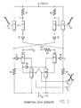
- FIG. 2 the preferred embodiment of the asymmetrical delay generator of the present invention is shown.
- This circuit is characterized by having two voltage sources, voltage source V CC and voltage V EE .
- Voltage V CC is approximately +1.4 volts while that at supply source V EE is approximately -2.2 volts.
- This circuit includes a first transistor T1 having its base coupled to an input terminal T A , its collector connected to the supply V CC and its emitter coupled to the node 1.
- a second transistor T2 has its base coupled to the input terminal T B , the collector coupled to the supply V CC and its emitter coupled to the node 2. It should be noted that the input terminals T A and T B of the circuit of the present invention are coupled to the T A and T B terminals in Fig.
- the circuit of Fig. 2 additionally includes a third transistor T3 whose base is also coupled to the terminal T A .
- the collector thereof is coupled to the base and to a resistor R1 which is disposed between the collector of transistor T3 and the voltage supply V CC .
- a fourth transistor T4 has its base coupled to the input terminal T B .
- the collector thereof is coupled the base thereof and also to a resistor R2 which is disposed between the collector of transistors T4 and the supply V CC .
- the emitter of transistor T3 is coupled to a Schottky diode S1 which is disposed between the emitter of transistor T3 and the node 2.
- the emitter of the transistor T4 is coupled to a second Schottky diode S2 which is disposed between the emitter of transistor T4 and the node 1.
- the circuit of Fig. 2 additionally includes a resistor R3 coupled between node 1 and the voltage supply V EE .
- a further resistor R4 is coupled between node 2 and the voltage supply V EE .
- the circuitry of Fig. 2 additionally includes a complementary transistor switch memory cell which comprises two pairs of transistors each coupled together in an SCR configuration.
- the first pair of transistors comprises transistors PR and NR and the second pair comprises the pair of transistors PL and NL.
- the transistor PR has its emitter coupled through a resistor R p to the supply V CC .
- the base of the transistor PR is coupled via a Schottky diode SR to the node 2 and also to the collector of transistor NR.
- the collector of the transistor PR is coupled to the base of the transistor NR.
- the base of the transistor NR is also coupled to the output terminal T D as well as to the collector of the transistor NL.
- the transistor PL has its emitter coupled to the voltage supply V EE .
- the base thereof is coupled by a Schottky diode SL to node 1.
- the base of the transistor PL is coupled to the collector of transistor NL, the base of the transistor NR and the output terminal T D .
- the collector of transistor PL is coupled to the base of the transistor NL which is further coupled to the collector of transistor NR and the output terminal T C .
- the connection between the collector of transistor PL and the base of transistor NL is coupled via a Schottky diode SS to the connection between the base of transistor PL and the collector of transistor NL.
- the emitter of transistor NL and transistor NR are both coupled directly to the voltage supply V EE .
- the circuitry of Fig. 2 operates in the following manner.
- the input signals to the circuitry of Fig. 2 at terminals T A and T B are received from the receiver 14 which has been described in the IBM Technical Disclosure Bulletin, Vol. 29, No. 7, December 1986, pp. 3148-3151.
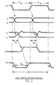
- That circuitry responds directly to a clock signal CLK, as illustrated in Fig. 3 which has a down portion CK DN and an up portion CK UP .
- Each clock cycle comprises the sum of the time CK DN plus CK UP .
- the change in the state of the CLK signal from its up to its down state comprises the beginning of the clock cycle.
- the receiver 14 In response to this transition, the receiver 14 produces a signal on the line T A which, sometime thereafter, changes from its up to its down state. In a similar fashion, the signal on the line T B transitions from its low to its high state in response to the clock signal CLK falling from its high to its low state. This is illustrated in Fig. 3.
- the circuitry of Fig. 2 includes transistors T1 and T2 which comprise emitter follower circuits which are used to write the CTS cell.
- Transistors T3 and the Schottky diode S1 form a cross-coupled feed back loop with transistor T4 and Schottky S2 to control the writing of the cell.
- Resistors R1 and R2 provide base drive current for the emitter followers T1 and T2 whereas the resistors R3 and R4 provide current pull-down on the nodes 1 and 2.
- the CTS cell contains two cross-coupled SCR devices each configured of a PNP and NPN transistor in an SCR connection.
- the two halves of the cell function differently.
- the right half of the cell namely diode SR and transistors PR and NR determine the turn on delay. That is, these elements determine the time between the state change on the lines T A and T B and when the signal at the output terminal T C completes its transition from a low to a high state.
- the right half of the cell is powered by a voltage supply V CC through a resistor RP. The value of that resistor can be changed to adjust the operating current level for the right half of the cell.
- That portion of the cell is switched from an on to an off state by driving transient current into the collector of the transistor NR from the emitter follower T2 and the Schottky diode SR.
- the time required to write this half-cell is a function of the SCR current level prior to its being written, the magnitude of the transient write current and the SCR device parameters such as the saturation capacitance C CB and the beta for the NPN transistor, etc.
- This turn on time is illustrated in Fig. 3 by the voltage T C rising from its low to its high state. Once this voltage reaches a given threshold voltage, the state of the voltage on the line T D begins to fall so that it reaches its down state at substantially the same time as the voltage on the line T C reaches its up state.
- the signal on the line DLY at the output of the level converter 24 goes from a low to a high state.
- this signal is input to the OR gate 18 of Fig. 1A, this causes the output on line PW to also go from its low to its high state.
- this turn on delay is ideally correlated to the time for the circuits coupled to the signal on the line PW to respond to the clock pulse thereon and have their state change, if such state change is called for.
- the speed of the circuitry within the delay generator is approximately that for the speed of writing the memory circuits coupled thereto.
- the delay generator of Fig. 1 As the delay generator of Fig. 1 has a memory cell in it, it must be reset before the beginning of the next clock cycle in order to be able to properly produce the output which will control the signal on the line PW. To accomplish this, as has already been pointed out, the circuit responds to the state change of the clock signal CLK going from its down to its up state to thereby cause the resetting of the cell within the delay generator circuit.
- the transition of the clock signal CLK from its down to its up state causes the receiver 14 to produce a change in the state of the signals on the lines T A and T B .
- This state change is responded to by the delay generator to produce a state change on the lines T C and T D thereby causing the signal DLY to go from its up to its down level.
- the turn off delay T OFF is determined by the circuit elements SL, PL and NL.
- the left half of the cell differs from the right half of the cell in two significant respects. In the first place, there is a Schottky diode coupled between the connection between the line coupling the collector of transistor PL to the base of transistor NL and the line coupling between the base of the transistor PL and the collector of the transistor NL. This prevents the SCR circuit including transistors PL and NL from operating in saturation.
- the second difference between the left and the right half of the cell is that the transistor PL is shut off to thereby reduce the storage charged within the SCR.
- the level converter 24 causes the output line DLY to go from its high to its low state which occurs, as illustrated in Fig. 3 well before the end of the cycle. Consequently, the delay generator of the present invention would allow the cycle time for the clock CLK to be reduced to a point where the next cycle could begin just after the time when the signal on the line DLY has gone from its high to its low state. As the turn off T OFF is quicker for the present circuit than can be achieved by the above mentioned prior art circuit, this means that the circuit of the present invention can function at a higher speed than the circuit illustrated in the prior art.
Landscapes
- Engineering & Computer Science (AREA)
- Physics & Mathematics (AREA)
- Theoretical Computer Science (AREA)
- Nonlinear Science (AREA)
- General Engineering & Computer Science (AREA)
- General Physics & Mathematics (AREA)
- Power Engineering (AREA)
- Pulse Circuits (AREA)
- Dram (AREA)
- Manipulation Of Pulses (AREA)
Applications Claiming Priority (2)
| Application Number | Priority Date | Filing Date | Title |
|---|---|---|---|
| US07/151,381 US4851711A (en) | 1988-02-02 | 1988-02-02 | Asymmetrical clock chopper delay circuit |
| US151381 | 1988-02-02 |
Publications (3)
| Publication Number | Publication Date |
|---|---|
| EP0328841A2 true EP0328841A2 (de) | 1989-08-23 |
| EP0328841A3 EP0328841A3 (en) | 1990-12-05 |
| EP0328841B1 EP0328841B1 (de) | 1993-10-13 |
Family
ID=22538511
Family Applications (1)
| Application Number | Title | Priority Date | Filing Date |
|---|---|---|---|
| EP88480089A Expired - Lifetime EP0328841B1 (de) | 1988-02-02 | 1988-12-06 | Asymmetrischer Verzögerungsgenerator für einen Taktzerhacker |
Country Status (4)
| Country | Link |
|---|---|
| US (1) | US4851711A (de) |
| EP (1) | EP0328841B1 (de) |
| JP (1) | JPH01205313A (de) |
| DE (1) | DE3884936T2 (de) |
Cited By (1)
| Publication number | Priority date | Publication date | Assignee | Title |
|---|---|---|---|---|
| WO2007115173A3 (en) * | 2006-03-31 | 2008-09-04 | Qualcomm Inc | Multimode, uniform-latency clock generation circuit |
Families Citing this family (7)
| Publication number | Priority date | Publication date | Assignee | Title |
|---|---|---|---|---|
| US5032740A (en) * | 1989-11-06 | 1991-07-16 | Eastman Kodak Company | Voltage level conversion of a clock signal |
| US5124573A (en) * | 1990-12-20 | 1992-06-23 | International Business Machines | Adjustable clock chopper/expander circuit |
| US5172010A (en) * | 1991-06-07 | 1992-12-15 | International Business Machines Corp. | Clock chopper/stretcher for high end machines |
| US5541882A (en) * | 1995-01-09 | 1996-07-30 | Texas Instruments Incorporated | Method of performing a column decode in a memory device and apparatus thereof |
| KR0147619B1 (ko) * | 1995-01-27 | 1998-12-01 | 김광호 | 플립플롭 제어기 |
| TW540073B (en) | 2001-10-19 | 2003-07-01 | Viewmove Technologies Inc | Electromagnetic mark device for a magnetism encoder |
| US7299374B2 (en) * | 2005-02-03 | 2007-11-20 | International Business Machines Corporation | Clock control method and apparatus for a memory array |
Family Cites Families (3)
| Publication number | Priority date | Publication date | Assignee | Title |
|---|---|---|---|---|
| US3165647A (en) * | 1962-06-20 | 1965-01-12 | Alpha Tronics Corp | Ring counter with no feedback comprising silicon controlled rectifier stages |
| US3351784A (en) * | 1965-07-19 | 1967-11-07 | Burroughs Corp | Multiple junction semiconductor device and circuit for increasing its speed of operation by saturation prevention |
| JPS55147038A (en) * | 1979-04-12 | 1980-11-15 | Fujitsu Ltd | Electronic circuit |
-
1988
- 1988-02-02 US US07/151,381 patent/US4851711A/en not_active Expired - Fee Related
- 1988-12-06 EP EP88480089A patent/EP0328841B1/de not_active Expired - Lifetime
- 1988-12-06 DE DE88480089T patent/DE3884936T2/de not_active Expired - Fee Related
- 1988-12-19 JP JP63318682A patent/JPH01205313A/ja active Granted
Non-Patent Citations (1)
| Title |
|---|
| IBM TECHNICAL DISCLOSURE BULLETIN. vol. 29, no. 7, 07 December 1986, NEW YORK US pages 3148 - 3151; "Clock chopper for complementary-transistor switch arrays" * |
Cited By (1)
| Publication number | Priority date | Publication date | Assignee | Title |
|---|---|---|---|---|
| WO2007115173A3 (en) * | 2006-03-31 | 2008-09-04 | Qualcomm Inc | Multimode, uniform-latency clock generation circuit |
Also Published As
| Publication number | Publication date |
|---|---|
| DE3884936D1 (de) | 1993-11-18 |
| JPH01205313A (ja) | 1989-08-17 |
| EP0328841B1 (de) | 1993-10-13 |
| EP0328841A3 (en) | 1990-12-05 |
| DE3884936T2 (de) | 1994-05-05 |
| JPH0552962B2 (de) | 1993-08-06 |
| US4851711A (en) | 1989-07-25 |
Similar Documents
| Publication | Publication Date | Title |
|---|---|---|
| JP3553988B2 (ja) | 同期ディジタル論理回路 | |
| US4777388A (en) | Fast latching flip-flop | |
| KR100301546B1 (ko) | 펄스발생회로 | |
| US5124573A (en) | Adjustable clock chopper/expander circuit | |
| JP2858134B2 (ja) | 複数のセンス増幅器への電力を制御する回路 | |
| EP0328841B1 (de) | Asymmetrischer Verzögerungsgenerator für einen Taktzerhacker | |
| US4761572A (en) | Semiconductor large scale integrated circuit with noise cut circuit | |
| US5012128A (en) | High speed push-pull driver having current mirror pull-down | |
| JPH022416A (ja) | 分布プリチヤージ・ワイヤor母線 | |
| US4274017A (en) | Cascode polarity hold latch having integrated set/reset capability | |
| US3231763A (en) | Bistable memory element | |
| EP0156477B1 (de) | Torschaltung zur Anwendung in einem Mikrocomputersystem | |
| JPH07107122A (ja) | デジタル信号伝送回路 | |
| US5172010A (en) | Clock chopper/stretcher for high end machines | |
| US6097642A (en) | Bus-line midpoint holding circuit for high speed memory read operation | |
| US6226222B1 (en) | Synchronous semiconductor memory device having a function for controlling sense amplifiers | |
| JPH04229490A (ja) | データ出力ドライバのデータ有効時間を延長する回路 | |
| US5760628A (en) | Circuit and method for generating pulses in response to the edges of an input signal | |
| US3010028A (en) | Asynchronous to synchronous pulse converter | |
| US3377518A (en) | Magnetostrictive delay line driver | |
| NL8302779A (nl) | Uitgangsbufferschakeling met drie toestanden. | |
| Perry et al. | A new and simple type of digital circuit technique using junction transistors and magnetic cores | |
| US4620119A (en) | Dual-mode timer circuit | |
| US2977576A (en) | Transistor timing circuit | |
| US5541545A (en) | High speed bipolar D latch circuit with reduced latch clocking output corruption |
Legal Events
| Date | Code | Title | Description |
|---|---|---|---|
| PUAI | Public reference made under article 153(3) epc to a published international application that has entered the european phase |
Free format text: ORIGINAL CODE: 0009012 |
|
| AK | Designated contracting states |
Kind code of ref document: A2 Designated state(s): DE FR GB |
|
| 17P | Request for examination filed |
Effective date: 19891214 |
|
| PUAL | Search report despatched |
Free format text: ORIGINAL CODE: 0009013 |
|
| AK | Designated contracting states |
Kind code of ref document: A3 Designated state(s): DE FR GB |
|
| 17Q | First examination report despatched |
Effective date: 19920519 |
|
| GRAA | (expected) grant |
Free format text: ORIGINAL CODE: 0009210 |
|
| AK | Designated contracting states |
Kind code of ref document: B1 Designated state(s): DE FR GB |
|
| REF | Corresponds to: |
Ref document number: 3884936 Country of ref document: DE Date of ref document: 19931118 |
|
| ET | Fr: translation filed | ||
| PLBE | No opposition filed within time limit |
Free format text: ORIGINAL CODE: 0009261 |
|
| STAA | Information on the status of an ep patent application or granted ep patent |
Free format text: STATUS: NO OPPOSITION FILED WITHIN TIME LIMIT |
|
| 26N | No opposition filed | ||
| PGFP | Annual fee paid to national office [announced via postgrant information from national office to epo] |
Ref country code: GB Payment date: 19951127 Year of fee payment: 8 |
|
| PGFP | Annual fee paid to national office [announced via postgrant information from national office to epo] |
Ref country code: FR Payment date: 19951128 Year of fee payment: 8 |
|
| PGFP | Annual fee paid to national office [announced via postgrant information from national office to epo] |
Ref country code: DE Payment date: 19951229 Year of fee payment: 8 |
|
| PG25 | Lapsed in a contracting state [announced via postgrant information from national office to epo] |
Ref country code: GB Effective date: 19961206 |
|
| GBPC | Gb: european patent ceased through non-payment of renewal fee |
Effective date: 19961206 |
|
| PG25 | Lapsed in a contracting state [announced via postgrant information from national office to epo] |
Ref country code: FR Effective date: 19970829 |
|
| PG25 | Lapsed in a contracting state [announced via postgrant information from national office to epo] |
Ref country code: DE Effective date: 19970902 |
|
| REG | Reference to a national code |
Ref country code: FR Ref legal event code: ST |