EP0325532B1 - Halbleiterphotodiode - Google Patents
Halbleiterphotodiode Download PDFInfo
- Publication number
- EP0325532B1 EP0325532B1 EP89400148A EP89400148A EP0325532B1 EP 0325532 B1 EP0325532 B1 EP 0325532B1 EP 89400148 A EP89400148 A EP 89400148A EP 89400148 A EP89400148 A EP 89400148A EP 0325532 B1 EP0325532 B1 EP 0325532B1
- Authority
- EP
- European Patent Office
- Prior art keywords
- layer
- light
- semiconductor
- content ratio
- substrate
- Prior art date
- Legal status (The legal status is an assumption and is not a legal conclusion. Google has not performed a legal analysis and makes no representation as to the accuracy of the status listed.)
- Expired - Lifetime
Links
Images



Classifications
-
- H—ELECTRICITY
- H10—SEMICONDUCTOR DEVICES; ELECTRIC SOLID-STATE DEVICES NOT OTHERWISE PROVIDED FOR
- H10F—INORGANIC SEMICONDUCTOR DEVICES SENSITIVE TO INFRARED RADIATION, LIGHT, ELECTROMAGNETIC RADIATION OF SHORTER WAVELENGTH OR CORPUSCULAR RADIATION
- H10F30/00—Individual radiation-sensitive semiconductor devices in which radiation controls the flow of current through the devices, e.g. photodetectors
- H10F30/20—Individual radiation-sensitive semiconductor devices in which radiation controls the flow of current through the devices, e.g. photodetectors the devices having potential barriers, e.g. phototransistors
- H10F30/21—Individual radiation-sensitive semiconductor devices in which radiation controls the flow of current through the devices, e.g. photodetectors the devices having potential barriers, e.g. phototransistors the devices being sensitive to infrared, visible or ultraviolet radiation
- H10F30/22—Individual radiation-sensitive semiconductor devices in which radiation controls the flow of current through the devices, e.g. photodetectors the devices having potential barriers, e.g. phototransistors the devices being sensitive to infrared, visible or ultraviolet radiation the devices having only one potential barrier, e.g. photodiodes
- H10F30/225—Individual radiation-sensitive semiconductor devices in which radiation controls the flow of current through the devices, e.g. photodetectors the devices having potential barriers, e.g. phototransistors the devices being sensitive to infrared, visible or ultraviolet radiation the devices having only one potential barrier, e.g. photodiodes the potential barrier working in avalanche mode, e.g. avalanche photodiodes
-
- H—ELECTRICITY
- H10—SEMICONDUCTOR DEVICES; ELECTRIC SOLID-STATE DEVICES NOT OTHERWISE PROVIDED FOR
- H10F—INORGANIC SEMICONDUCTOR DEVICES SENSITIVE TO INFRARED RADIATION, LIGHT, ELECTROMAGNETIC RADIATION OF SHORTER WAVELENGTH OR CORPUSCULAR RADIATION
- H10F30/00—Individual radiation-sensitive semiconductor devices in which radiation controls the flow of current through the devices, e.g. photodetectors
- H10F30/20—Individual radiation-sensitive semiconductor devices in which radiation controls the flow of current through the devices, e.g. photodetectors the devices having potential barriers, e.g. phototransistors
- H10F30/21—Individual radiation-sensitive semiconductor devices in which radiation controls the flow of current through the devices, e.g. photodetectors the devices having potential barriers, e.g. phototransistors the devices being sensitive to infrared, visible or ultraviolet radiation
- H10F30/22—Individual radiation-sensitive semiconductor devices in which radiation controls the flow of current through the devices, e.g. photodetectors the devices having potential barriers, e.g. phototransistors the devices being sensitive to infrared, visible or ultraviolet radiation the devices having only one potential barrier, e.g. photodiodes
- H10F30/225—Individual radiation-sensitive semiconductor devices in which radiation controls the flow of current through the devices, e.g. photodetectors the devices having potential barriers, e.g. phototransistors the devices being sensitive to infrared, visible or ultraviolet radiation the devices having only one potential barrier, e.g. photodiodes the potential barrier working in avalanche mode, e.g. avalanche photodiodes
- H10F30/2255—Individual radiation-sensitive semiconductor devices in which radiation controls the flow of current through the devices, e.g. photodetectors the devices having potential barriers, e.g. phototransistors the devices being sensitive to infrared, visible or ultraviolet radiation the devices having only one potential barrier, e.g. photodiodes the potential barrier working in avalanche mode, e.g. avalanche photodiodes in which the active layers form heterostructures, e.g. SAM structures
-
- H—ELECTRICITY
- H10—SEMICONDUCTOR DEVICES; ELECTRIC SOLID-STATE DEVICES NOT OTHERWISE PROVIDED FOR
- H10F—INORGANIC SEMICONDUCTOR DEVICES SENSITIVE TO INFRARED RADIATION, LIGHT, ELECTROMAGNETIC RADIATION OF SHORTER WAVELENGTH OR CORPUSCULAR RADIATION
- H10F77/00—Constructional details of devices covered by this subclass
- H10F77/10—Semiconductor bodies
- H10F77/12—Active materials
- H10F77/124—Active materials comprising only Group III-V materials, e.g. GaAs
- H10F77/1243—Active materials comprising only Group III-V materials, e.g. GaAs characterised by the dopants
-
- H—ELECTRICITY
- H10—SEMICONDUCTOR DEVICES; ELECTRIC SOLID-STATE DEVICES NOT OTHERWISE PROVIDED FOR
- H10F—INORGANIC SEMICONDUCTOR DEVICES SENSITIVE TO INFRARED RADIATION, LIGHT, ELECTROMAGNETIC RADIATION OF SHORTER WAVELENGTH OR CORPUSCULAR RADIATION
- H10F77/00—Constructional details of devices covered by this subclass
- H10F77/10—Semiconductor bodies
- H10F77/12—Active materials
- H10F77/124—Active materials comprising only Group III-V materials, e.g. GaAs
- H10F77/1248—Active materials comprising only Group III-V materials, e.g. GaAs having three or more elements, e.g. GaAlAs, InGaAs or InGaAsP
-
- Y—GENERAL TAGGING OF NEW TECHNOLOGICAL DEVELOPMENTS; GENERAL TAGGING OF CROSS-SECTIONAL TECHNOLOGIES SPANNING OVER SEVERAL SECTIONS OF THE IPC; TECHNICAL SUBJECTS COVERED BY FORMER USPC CROSS-REFERENCE ART COLLECTIONS [XRACs] AND DIGESTS
- Y02—TECHNOLOGIES OR APPLICATIONS FOR MITIGATION OR ADAPTATION AGAINST CLIMATE CHANGE
- Y02E—REDUCTION OF GREENHOUSE GAS [GHG] EMISSIONS, RELATED TO ENERGY GENERATION, TRANSMISSION OR DISTRIBUTION
- Y02E10/00—Energy generation through renewable energy sources
- Y02E10/50—Photovoltaic [PV] energy
- Y02E10/544—Solar cells from Group III-V materials
Definitions
- This invention relates to a semiconductor avalanche photo-diode (referred to hereinafter as APD). More particularly, it relates to an APD capable of low noise as well as high speed operation.
- APD semiconductor avalanche photo-diode
- the numeral 1 denotes an n+-type GaSb substrate
- the numeral 2 denotes an n-type GaSb light absorbing layer
- the numeral 4A denotes an n ⁇ -type Al x Ga 1-x Sb window layer 3
- the numeral 5 denotes a p+-type region doped in the window layer for forming a pn-junction, while some thickness of the window layer 4A is left between the pn junction 5′ and the avalanche multiplication layer 3; and a light to be detected is injected through the p+-type region 5 into the light absorbing layer 2.
- the above-described material of the avalanche multiplication layer 3 generates a high ionization rate of positive holes to that of electrons by a resonant impact ionization phenomena, resulting in an achievement of low noise and high speed operation of the APD.
- the resonant impact ionization is disclosed by O. Hilderbrand et al. in IEEE Journal of Quantum Electronics, vol. QE-17, No.2, p284-288, Feb. 1981.
- FIG. 2 characteristics of quantum efficiency, which is an average number of electrons or positive holes photoelectrically emitted in a photoelectric material per incidental photon (i.e. a unit intensity of light) versus the incidental wave length, is presented.
- the incidental light having 1.3 »m wavelength produces both carriers, i.e. electrons and positive holes, in the avalanche multiplication layer 3 having x of 0.065, as indicated by a mark "M", even though the light should pass therethrough without producing carriers therein.
- FIG. 3 Another prior art APD disclosed by the same assignee in Japanese unexamined patent publication Sho 60-105281 is schematically illustrated in FIG. 3, where the numeral 3-11 denotes a p+-type GaSb substrate; the numeral 3-12 denotes a p-type Ga 0.935 Al 0.065 Sb avalanche multiplication layer which generates a resonant impact ionization phenomena; the numeral 3-13 denotes a p-type Ga 0.9 Al 0.1 Sb light absorbing layer; the numeral 3-14 denotes a p-type Ga 0.6 Al 0.4 Sb window layer; the numeral 3-15 denotes an n+-type region doped in the window layer for forming a pn junction; the numeral 3-18 denotes an anti-reflection layer; and the numerals 3-19 and 3-20 denote electrodes for applying a bias voltage to the APD.
- the numeral 3-11 denotes a p+-type GaSb substrate
- the light to be detected is injected through the n+ region 3-15 into the light absorbing layer 3-13, and accordingly, does not have to pass through the avalanche multiplication layer 3-12. Therefore, the problem of the first prior art APD is avoided.
- other problems are thereby created. Because the pn junction is located far from the avalanche multiplication layer 3-12, fluctuations of the impurity density or the thickness, etc., of the layers therebetween in the fabrication process seriously affect the APD characteristics.
- Furthermore, there are difficulties in designing and fabricating the n+ region for instance, with currently available diffusion source materials, such as sulfur or selenium, for forming the n+ region, it is difficult to achieve an adequate diffusion depth.
- a third prior art APD is schematically illustrated in FIG. 4, where the same or like numerals denote the same or corresponding devices of FIG. 1.
- a substrate 1, and a light absorbing layer 2 are the same as those of FIG. 1.
- An avalanche multiplication layer 3′ is formed of the same material in the same way as in FIG. 1, but in a mesa shape.
- a peripheral portion of the mesa is filled with the same material as that of the window layer 4A, so as to form a guard-ring 4B.
- zinc is diffused approximately 1 »m deep to form a p+-type region 5.
- the p+-type region 5 forms a pn junction 5′ in the avalanche multiplication layer 3′ as well as in the guard-ring 4B.
- a light to be detected is injected through the p+-type region 5 into the light absorbing layer 2.
- the problem of the third prior art APD is the same as that of the first prior art APD shown in FIG. 1.
- Another type of avalanche photodiode disclosed in US-A-4 110 778 has an inverted structure so that light enters through the substrate side of the device. The light energy is absorbed as it enters the active region where a high field p-n junction is created.
- the light enters through a large bandgap window layer located at a side opposite the substrate.
- the multiplication takes place in a layer between the window layer and an absorbing layer having a bandgap smaller than that of the window layer.
- This configuration is intended to reduce the field intensity at the light absorbing layer to reduce dark current.
- the avalanche multiplication layer of the present photodiode has an aluminum content chosen so as to produce a high ionization rate ratio, by a resonant impact ionization phenomena, generated with only the positive carriers by an electric field induced from the pn junction being located close (i.e. directly or only via the surface layer) to the avalanche multiplication layer; therefore, resulting in a low noise and high speed operation of the APD.
- FIG. 1 schematically illustrates a prior art APD.
- FIG. 2 shows quantum efficiency versus incidental wave length for various aluminum content ratio of Al x Ga l-x Sb.
- FIG. 3 schematically illustrates a second prior art APD.
- FIG. 4 schematically illustrates a third prior art APD.
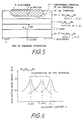
- FIG. 5 schematically illustrates a cross-sectional side view of a preferred embodiment of the present invention.
- FIG. 6 is a graph of the effect of aluminum content on ionization rate ratio.
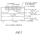
- FIG. 7 schematically illustrates a cross-sectional side view of a second preferred embodiment of the present invention.
- FIG. 8 shows a comparison of noise figures achieved by an APD of the present invention with a prior art APD.
- LPE liquid phase epitaxy
- a source can be automatically supplemented into the melt to form a thick substrate.
- a light absorbing layer 2 is formed of an n-type GaSb (gallium antimony) doped typically with tellurium having a concentration of an impurity such as LPE, typically of approximately 5 x 1015cm ⁇ 3, as thick as approximately from 2 to 3 »m, on the semiconductor substrate 1A by a widely known method.
- LPE gallium antimony
- An avalanche multiplication layer 3 is formed of an n-type Al x Ga l-x Sb, where x is approximately from 0.02 to 0.1, typically approximately 0.065, doped typically with tellurium having a concentration of an impurity such as LPE, typically 5 x 1015cm ⁇ 3, as thick as approximately 1 »m on the light absorbing layer 2 by a widely known method.
- a surface layer 4A is formed of an n ⁇ -type Al x Ga l-x Sb, where x is from 0.1 to 0.3, doped typically with tellurium having a concentration of an impurity such as LPE of 5 x 1015cm ⁇ 3 maximum, typically 2 x 1015cm ⁇ 3, as thick as approximately from 2 to 3 »m on the avalanche multiplication layer 3 by a widely known method.
- a p+-type region 5 having an impurity concentration, typically approximately 1019cm ⁇ 3 is formed approximately 1 »m deep for forming a pn junction 5′ in the surface layer 4A, while an approximately 1 »m thickness of the surface layer 4A is left between the pn junction 5′ and the avalanche multiplication layer 3.
- the p+-type region 5 is formed by a widely known method, such as diffusion of zinc or ion implantation of beryllium.
- a ring shaped electrode 7 is formed by depositing typically Au/AuGe (gold and gold-germanium alloy) as thick as 2700/300 ⁇ for each material, on a surface, opposite to the light absorbing layer 2, of the substrate 1A, for connecting a return of the bias voltage. Through an opening at the centre portion of the electrode 7, the incidental light is injected into a portion to receive the light on the substrate 1A.
- the quantum efficiency of the wave length now in consideration for a practical communication use i.e. mainly 1.3 and 1.55 »m
- the incidental light passes through the substrate while producing essentially no carriers therein.
- the light having passed through the substrate 1A enters into the light absorbing layer 2, where sufficient carriers are produced for a wide range of wave lengths, i.e. for both 1.3 and 1.55 »m wave lengths, as represented by curve (2) having sufficient quantum efficiency in FIG. 2.
- the carriers produced in the light absorbing layer 2 are both the positive holes ph and electrons e as denoted in FIG. 5.
- the produced positive hole ph is accelerated by the electric field induced by the applied bias voltage into the avalanche multiplication layer 3.
- the aluminum content x is particularly chosen so that an ionization rate ratio ⁇ / ⁇ indicates an ionization rate of the positive holes produced therein and ⁇ indicates an ionization rate of the electrons produced therein) is remarkably increased. This is known as resonant impact ionization.
- Resonant impact ionization is a phenomena in which the spin orbit splitting ⁇ of the valence band becomes equal (thus called resonant) to the band gap energy E g between the conduction band and the valence band.
- resonant the spin orbit splitting ⁇ of the valence band becomes equal
- E g the band gap energy
- ⁇ / ⁇ the ionization rate ratio
- the greater the value of the ionization rate ratio the greater the reduction in the fluctuation noise produced in the APD, and the faster the operation of the APD.
- the particular aluminum content ratio optimum for the maximum ionization rate ratio varies from 0.02 to 0.1, typically 0.065 as shown in FIG. 6.
- the ionization rate ratio can be as high as 20 or more.
- the band gap energy of the substrate 1A is more the 1 eV.
- Band gap energy of the light-absorbing layer is typically 0.72 eV.
- the band gap energy of the avalanche multiplication layer 3 is typically 0.8 to 0.83 eV. Because an absorption edge of the quantum efficiency curve is inversely proportional to the band gap energy of the material as shown in FIG. 2, the high band gap energy of the substrate 1A allows the light to pass therethrough while generating no carriers therein.
- the band gap energy of the avalanche multiplication layer 3 allows for the generation of the resonant impact ionization.
- the surface layer 4A formed of Al x Ga l-x Sb, where x is from 0.1 to 0.3, has a lower impurity concentration as well as a lower ionization rate than the avalanche multiplication layer 3, resulting in a relatively high avalanche breakdown voltage, for example, more than 50 V, and also in the reduction of the concentration of electric field at peripheral portion 5 ⁇ of the pn junction, the surface layer 4A contributes to reduce a tunnel current flowing therethrough, i.e. a dark current of the APD, even though a guard-ring, which has been widely employed in APD's in order to reduce the peripheral electric field concentration, is not provided in the APD of the embodiment shown in FIG. 4.
- a second preferred embodiment of the present invention is hereinafter described, referring to FIG. 7, where the same or like numerals denote the same or corresponding devices.
- the substrate 1A and the light absorbing layer 2 are essentially the same and act respectively the same as those of the first preferred embodiment shown in FIG. 5.
- An avalanche multiplication layer 3 ⁇ is formed of the same material as that of the first embodiment and as thick as, for example, 0.5 to 1.0 »m on the light absorbing layer 2 in essentially the same way as that of FIG. 5.
- a peripheral portion of the deposited avalanche multiplication layer 3 ⁇ is removed by a chemical etching so as to leave a mesa of the avalanche multiplication layer 3 ⁇ , while the centre portion is masked with a resist mask (not shown in the figure).
- a guard-ring 4B is formed on the etched peripheral portion by filling with an n ⁇ -type Al x Ga l-x Sb having x of approximately 0.3 doped with, for example, tellurium of as low impurity concentration as 5 x 1015cm ⁇ 3 maximum, typically 2 x 1015cm ⁇ 3, typically by a widely used LPE technique, while the mask is left on the mesa.
- a positive dopant is doped into the surfaces of the avalanche multiplication layer 3 ⁇ as well as the adjacent part of the guardring 4B approximately 1 »m deep typically by diffusing zinc or ion implanting beryllium, to a concentration of as much as typically 1019cm ⁇ 3, as denoted with the hatched area 5.
- the p+ region 5 forms a pn junction 5′ in the avalanche multiplication layer 3 ⁇ and the guard-ring 4B.
- the peripheral portion 5 ⁇ of the pn junction is located in the low impurity-doped guard-ring 4B having a low ionization rate, the undesirably low voltage avalanche breakdown caused by an electric field concentration at the peripheral portion can be prevented. Accordingly, the avalanche breakdown takes place only at the centre portion having no undesirable electric field concentration.
- the direct contact of the pn junction with the avalanche multiplication layer 3 ⁇ is advantageous for inducing a high electric field intensity in the avalanche multiplication layer 3 ⁇ .
- an APD of the present invention achieved a noise as low as 3.8 compared with 6 to 9 of a prior art APD.
- the Al x Ga l-x Sb for the layers 1A, 3 and/or 4 may be replaced with Al x Ga l-x Sb y As l-y (aluminum gallium antimony arsenic) in order to achieve better matching of the lattice constant with the GaSb.
- Values of y are chosen: for example, 0.01 to 0.03 in the substrate; typically from 0.002 to 0.01 in the avalanche multiplication layer; and typically from 0.01 to 0.03 in surface layer 4A or the guard-ring 4B.
- the value of the content ratio y has essentially no effect on the above-described characteristics having various values of aluminum content x.
- the electrode 7 is formed in a ring shape so that the light is injected through the opening into the substrate 1A, it is apparent that the structure of the electrode 7 is arbitrarily chosen as long as the bias voltage is properly applied to the APD device.
- the design of the electric field in the avalanche multiplication layer is facilitated as compared with the prior art APD structures.
Landscapes
- Light Receiving Elements (AREA)
Claims (7)
- Halbleiterphotodiode enthaltend:
ein Basisschichtsubstrat (1A), das hergestellt ist aus einem Halbleiter mit einer ersten Bandabstandsenergie und mit einer ersten Oberfläche zur Aufnahme von Licht und einer der ersten Oberfläche entgegengesetzten zweiten Oberfläche;
eine lichtabsorbierende Schicht (2), die hergestellt ist aus einem Halbleiter mit einer zweiten Bandabstandsenergie und auf der zweiten Oberfläche der Basisschicht gebildet ist, wobei das zweite Band so gewählt ist, daß die lichtabsorbierende Schicht das Licht aufnimmt und Träger entsprechend der Intensität des aufgenommenen Lichts erzeugt;
eine Avalanchevervielfachungsschicht (3), die hergestellt ist aus AlxGa1-xSb oder AlxGa1-xSbyAs1-y mit einer dritten Bandabstandsenergie, wobei das Aluminiumgehaltsverhältnis x von 0,02 bis 0,1 beträgt und das Antimongehaltsverhältnis y 0 < y ≦ 1 ist, und die auf der lichtabsorbierenden Schicht ausgebildet ist, wobei das Aluminiumgehaltsverhältnis x in der Avalanchevervielfachungsschicht so gewählt ist, daß durch ein Resonanzstoßionisationsphänomen ein maximales Ionisationsratenverhältnis von positiven Löchern zu Elektronen erzeugt wird;
eine Oberflächenschicht (4A), die aus einem Halbleiter hergestellt und auf der Vervielfachungsschicht (3; 3˝) gebildet ist;
einen Fremdstoffbereich (5), der in der Oberflächenschicht auf einer der Vervielfachungsschicht entgegengesetzten Oberfläche ausgebildet ist und einen dem der Oberflächenschicht entgegengesetzten Leitfähigkeitstyp hat;
eine erste Elektrode (7), die auf der ersten Oberfläche der Basisschicht ausgebildet ist, zum Anlegen einer Vorspannung, wobei die erste Elektrode so geformt ist, daß sie einen Einfall des Lichts in eine lichtaufnehmende Region des Substrats gestattet; und
eine zweite Elektrode (6), die auf dem Fremdstoffbereich ausgebildet ist, zum Anlegen der Vorspannung;
wobei die erste Bandabstandsenergie größer ist als die zweiten und dritten Bandabstandsenergien. - Halbleiterphotodiode nach Anspruch 1, bei welcher:
das Substrat (1A) aus einem n-Typ-AlxGa1-xSb- oder AlxGa1-xSbyAs1-y-Halbleiter gebildet ist, wobei das Aluminiumgehaltsverhältnis x von 0,1 bis 0,3 beträgt und das Antimongehaltsverhältnis y 0 < y ≦ 1 ist;
die lichtabsorbierende Schicht (2) aus einem n-Typ-GaSb-Halbleiter gebildet ist;
die Oberflächenschicht (4A) aus einem n-Typ-AlxGa1-xSb- oder AlxGa1-xSbyAs1-y-Halbleiter gebildet ist, wobei das Aluminiumgehaltsverhältnis x 0 < x < 1 ist und darüber hinaus größer als der Aluminiumgehalt x in der Vervielfachungsschicht (3) ist und das Antimongehaltsverhältnis y 0 < y ≦ 1 ist; und
der Fremdstoffbereich (5) aus einem in der Oberflächenschicht dotierten p-Typ-Halbleiter gebildet ist. - Halbleiterphotodiode enthaltend:
ein Substrat (1A), das aus einem n-Typ-AlxGa1-xSb- oder AlxGa1-xSbyAs1-y-Halbleiter gebildet ist, mit einer ersten Bandabstandsenergie, wobei das Aluminiumgehaltsverhältnis x von 0,02 bis 0,1 beträgt und das Antimongehaltsverhältnis y 0 < y ≦ 1 ist, wobei eine erste Oberfläche des Substrats Licht aufnimmt;
eine lichtabsorbierende Schicht (2), die aus einem n-Typ-GaSb-Halbleiter gebildet ist;
und weiterhin enthaltend:
eine lichtabsorbierende Schicht (2), die aus einem n-Typ-GaSb-Halbleiter auf einer zweiten Oberfläche gebildet ist, die der ersten Oberfläche des Substrats entgegengesetzt ist, wobei die lichtabsorbierende Schicht das durch das Substrat hindurchtretende Licht aufnimmt, so daß es der Intensität des aufgenommenen Lichts entsprechende Träger erzeugt;
eine Vervielfachungsschicht (3˝), die aus einem n-Typ-AlxGa1-xSb- oder AlxGa1-xSbyAs1-y-Halbleiter gebildet ist, wobei das Aluminiumgehaltsverhältnis x von 0,02 bis 0,1 beträgt und das Antimongehaltsverhältnis y 0 < y ≦ 1 ist, auf der lichtabsorbierenden Schicht, wobei das Aluminiumgehaltsverhältnis x in der Vervielfachungsschicht so gewählt ist, daß durch ein Resonanzstoßionisationsphänomen ein maximales Ionisationsratenverhältnis von positiven Löchern zu Elektronen erzeugt wird, wobei die Dicke eines Umfangsbereichs der Vervielfachungsschicht dünner ist als ein zentraler Bereich der Vervielfachungsschicht;
einen Schutzringbereich (4B), der aus einem n-Typ-AlxGa1-xSb- oder AlxGa1-xSbyAs1-y-Halbleiter gebildet ist, wobei das Aluminiumgehaltsverhältnis x 0 < x < 1 ist und darüber hinaus größer ist als der Aluminiumgehalt x in der Vervielfachungsschicht (3˝) und das Antimongehaltsverhältnis y 0 < y ≦ 1 ist, auf dem dünnen peripheren Bereich der Vervielfachungsschicht (3˝), koplanar mit der Oberfläche des zentralen Bereichs der Vervielfachungsschicht;
einen Fremdstoffbereich (5), der aus einem in der Vervielfachungsschicht und in einem benachbarten Bereich des Schutzringbereichs dotierten p-Typ-Halbleiter an der lichtabsorbierenden Schicht entgegengesetzten Oberflächen gebildet ist;
eine erste Elektrode (7), die auf der ersten Oberfläche des Substrats gebildet ist, zum Anlegen einer Spannung, wobei die erste Elektrode so geformt ist, daß sie einen Einfall des Lichts in eine lichtaufnehmende Region des Substrats gestattet;
eine zweite Elektrode (6), die auf dem Fremdstoffbereich gebildet ist, zum Anlegen einer positiven Spannung in Bezug zu der der ersten Elektrode angelegten Spannung. - Photodiode nach Anspruch 1 oder 3, bei welcher das Aluminiumgehaltsverhältnis x in der Avalanchevervielfachungsschicht (3; 3˝) ungefähr 0,065 ist.
- Photodiode nach Anspruch 1, bei welcher in der Oberflächenschicht (4A) das Aluminiumgehaltsverhältnis x von 0,1 bis 0,3 beträgt und die Fremdstoffkonzentration niedriger als ungefähr 5 x 10¹⁵cm⁻³ ist.
- Photodiode nach Anspruch 1 oder 3, bei der die erste Photodiode (7) durch eine Niederschlagung von metallischem Material gebildet ist.
- Photodiode nach Anspruch 1 oder 3, bei welcher die zweite Elektrode (6) durch eine Niederschlagung von metallischem Material gebildet ist.
Applications Claiming Priority (2)
| Application Number | Priority Date | Filing Date | Title |
|---|---|---|---|
| JP63007702A JPH01183174A (ja) | 1988-01-18 | 1988-01-18 | 半導体受光素子 |
| JP7702/88 | 1988-01-18 |
Publications (3)
| Publication Number | Publication Date |
|---|---|
| EP0325532A2 EP0325532A2 (de) | 1989-07-26 |
| EP0325532A3 EP0325532A3 (en) | 1990-05-23 |
| EP0325532B1 true EP0325532B1 (de) | 1995-04-12 |
Family
ID=11673086
Family Applications (1)
| Application Number | Title | Priority Date | Filing Date |
|---|---|---|---|
| EP89400148A Expired - Lifetime EP0325532B1 (de) | 1988-01-18 | 1989-01-18 | Halbleiterphotodiode |
Country Status (5)
| Country | Link |
|---|---|
| US (1) | US4984032A (de) |
| EP (1) | EP0325532B1 (de) |
| JP (1) | JPH01183174A (de) |
| KR (1) | KR910009357B1 (de) |
| DE (1) | DE68922117T2 (de) |
Families Citing this family (16)
| Publication number | Priority date | Publication date | Assignee | Title |
|---|---|---|---|---|
| US5179430A (en) * | 1988-05-24 | 1993-01-12 | Nec Corporation | Planar type heterojunction avalanche photodiode |
| JPH01296676A (ja) * | 1988-05-24 | 1989-11-30 | Nec Corp | 半導体受光装置 |
| US5138416A (en) * | 1991-07-12 | 1992-08-11 | Xerox Corporation | Multi-color photosensitive element with heterojunctions |
| US5148251A (en) * | 1991-11-25 | 1992-09-15 | The United States Of America As Represented By The Secretary Of The Army | Photoconductive avalanche GaAs switch |
| GB0030204D0 (en) | 2000-12-12 | 2001-01-24 | Secr Defence | Reduced noise semiconductor photodetector |
| US6914314B2 (en) * | 2003-01-31 | 2005-07-05 | Foveon, Inc. | Vertical color filter sensor group including semiconductor other than crystalline silicon and method for fabricating same |
| JP5015494B2 (ja) * | 2006-05-22 | 2012-08-29 | 住友電工デバイス・イノベーション株式会社 | 半導体受光素子 |
| EP2073277A1 (de) * | 2007-12-19 | 2009-06-24 | Alcatel Lucent | Lawinenphotodiode |
| FR3000608B1 (fr) | 2012-12-31 | 2015-03-06 | Commissariat Energie Atomique | Structure semiconductrice du type photodiode a avalanche et procede de fabrication d'une telle structure |
| FR3000610B1 (fr) | 2012-12-31 | 2015-03-06 | Commissariat Energie Atomique | Structure semiconductrice du type photodiode a avalanche a faible temps de reponse et procede de fabrication d'une telle photodiode |
| FR3000609B1 (fr) | 2012-12-31 | 2015-01-30 | Commissariat Energie Atomique | Structure semiconductrice du type photodiode a avalanche a haut rapport signal sur bruit et procede de fabrication d'une telle photodiode |
| US9893227B2 (en) * | 2013-05-24 | 2018-02-13 | The United States Of America As Represented By The Secretary Of The Army | Enhanced deep ultraviolet photodetector and method thereof |
| FR3021807B1 (fr) | 2014-05-27 | 2017-09-29 | Commissariat A L Energie Atomique Et Aux Energies Alternatives | Matrice de photodiodes mesa a ftm amelioree |
| US10381502B2 (en) * | 2015-09-09 | 2019-08-13 | Teledyne Scientific & Imaging, Llc | Multicolor imaging device using avalanche photodiode |
| CN106887469B (zh) * | 2017-03-22 | 2019-05-07 | 武汉光谷量子技术有限公司 | 一种雪崩二极管的外延结构及雪崩二极管的制造方法 |
| US20240047602A1 (en) * | 2022-08-08 | 2024-02-08 | Apple Inc. | Electromagnetic Radiation Detector with Reduced Dark Current |
Family Cites Families (8)
| Publication number | Priority date | Publication date | Assignee | Title |
|---|---|---|---|---|
| US4110778A (en) * | 1977-06-21 | 1978-08-29 | The United States Of America As Represented By The Secretary Of The Air Force | Narrow-band inverted homo-heterojunction avalanche photodiode |
| US4203124A (en) * | 1978-10-06 | 1980-05-13 | Bell Telephone Laboratories, Incorporated | Low noise multistage avalanche photodetector |
| US4403397A (en) * | 1981-07-13 | 1983-09-13 | The United States Of America As Represented By The Secretary Of The Navy | Method of making avalanche photodiodes |
| KR900000074B1 (ko) * | 1981-10-02 | 1990-01-19 | 미쓰다 가쓰시게 | 광 검출용 반도체장치 |
| JPS60105281A (ja) * | 1983-11-11 | 1985-06-10 | Fujitsu Ltd | 半導体受光装置 |
| CA1228662A (en) * | 1984-04-10 | 1987-10-27 | Paul P. Webb | Double mesa avalanche photodetector |
| JPS611064A (ja) * | 1984-05-31 | 1986-01-07 | Fujitsu Ltd | 半導体受光装置 |
| JPS62259481A (ja) * | 1986-04-15 | 1987-11-11 | Fujitsu Ltd | 半導体受光装置 |
-
1988
- 1988-01-18 JP JP63007702A patent/JPH01183174A/ja active Pending
-
1989
- 1989-01-07 KR KR1019890000138A patent/KR910009357B1/ko not_active Expired
- 1989-01-17 US US07/297,391 patent/US4984032A/en not_active Expired - Fee Related
- 1989-01-18 EP EP89400148A patent/EP0325532B1/de not_active Expired - Lifetime
- 1989-01-18 DE DE68922117T patent/DE68922117T2/de not_active Expired - Fee Related
Also Published As
| Publication number | Publication date |
|---|---|
| JPH01183174A (ja) | 1989-07-20 |
| US4984032A (en) | 1991-01-08 |
| DE68922117T2 (de) | 1995-08-24 |
| KR910009357B1 (ko) | 1991-11-12 |
| EP0325532A3 (en) | 1990-05-23 |
| KR890012403A (ko) | 1989-08-26 |
| DE68922117D1 (de) | 1995-05-18 |
| EP0325532A2 (de) | 1989-07-26 |
Similar Documents
| Publication | Publication Date | Title |
|---|---|---|
| EP0325532B1 (de) | Halbleiterphotodiode | |
| EP0163546B1 (de) | Herstellungsverfahren einer Lawinenphotodiode und so hergestellte Lawinenphotodiode | |
| US5190883A (en) | Method for making an integrated light guide detector structure made of a semiconductive material | |
| US4651187A (en) | Avalanche photodiode | |
| EP0675549B1 (de) | Lawinenphotodiode mit Übergitter | |
| EP0156156A1 (de) | Avalanche-Photodioden | |
| EP0163295B1 (de) | Halbleiterphotodetektor und Verfahren zu seiner Herstellung | |
| KR980012624A (ko) | 반도체소자 및 반도체소자의 제조방법 | |
| JPS631079A (ja) | 半導体受光素子およびその製造方法 | |
| JP3828982B2 (ja) | 半導体受光素子 | |
| JPH04111477A (ja) | 受光素子 | |
| US5315148A (en) | Photo-sensing device | |
| US4587544A (en) | Avalanche photodetector | |
| US4935795A (en) | Avalanche photodiode with uniform avalanche multiplication | |
| EP0076495B1 (de) | Fotodiode | |
| CA1228663A (en) | Photodetector with isolated avalanche region | |
| US5391910A (en) | Light receiving device | |
| US5343054A (en) | Semiconductor light-detection device with recombination rates | |
| JPH038117B2 (de) | ||
| US4561007A (en) | Double mesa avalanche photodetector | |
| CA1280196C (en) | Avanlanche photodiode | |
| US4816890A (en) | Optoelectronic device | |
| US4586066A (en) | Avalanche photodetector | |
| CA1285642C (en) | Vertical photoconductive detector | |
| US4918508A (en) | Vertical photoconductive detector |
Legal Events
| Date | Code | Title | Description |
|---|---|---|---|
| PUAI | Public reference made under article 153(3) epc to a published international application that has entered the european phase |
Free format text: ORIGINAL CODE: 0009012 |
|
| AK | Designated contracting states |
Kind code of ref document: A2 Designated state(s): DE FR GB |
|
| PUAL | Search report despatched |
Free format text: ORIGINAL CODE: 0009013 |
|
| AK | Designated contracting states |
Kind code of ref document: A3 Designated state(s): DE FR GB |
|
| 17P | Request for examination filed |
Effective date: 19901009 |
|
| 17Q | First examination report despatched |
Effective date: 19930129 |
|
| GRAA | (expected) grant |
Free format text: ORIGINAL CODE: 0009210 |
|
| AK | Designated contracting states |
Kind code of ref document: B1 Designated state(s): DE FR GB |
|
| REF | Corresponds to: |
Ref document number: 68922117 Country of ref document: DE Date of ref document: 19950518 |
|
| ET | Fr: translation filed | ||
| PGFP | Annual fee paid to national office [announced via postgrant information from national office to epo] |
Ref country code: GB Payment date: 19951124 Year of fee payment: 8 |
|
| PGFP | Annual fee paid to national office [announced via postgrant information from national office to epo] |
Ref country code: FR Payment date: 19951127 Year of fee payment: 8 |
|
| PLBI | Opposition filed |
Free format text: ORIGINAL CODE: 0009260 |
|
| PLBF | Reply of patent proprietor to notice(s) of opposition |
Free format text: ORIGINAL CODE: EPIDOS OBSO |
|
| 26 | Opposition filed |
Opponent name: ALCATEL SEL AKTIENGESELLSCHAFT Effective date: 19960112 |
|
| PGFP | Annual fee paid to national office [announced via postgrant information from national office to epo] |
Ref country code: DE Payment date: 19960321 Year of fee payment: 8 |
|
| PLBF | Reply of patent proprietor to notice(s) of opposition |
Free format text: ORIGINAL CODE: EPIDOS OBSO |
|
| PLBF | Reply of patent proprietor to notice(s) of opposition |
Free format text: ORIGINAL CODE: EPIDOS OBSO |
|
| PG25 | Lapsed in a contracting state [announced via postgrant information from national office to epo] |
Ref country code: GB Effective date: 19970118 |
|
| GBPC | Gb: european patent ceased through non-payment of renewal fee |
Effective date: 19970118 |
|
| PG25 | Lapsed in a contracting state [announced via postgrant information from national office to epo] |
Ref country code: FR Effective date: 19970930 |
|
| PG25 | Lapsed in a contracting state [announced via postgrant information from national office to epo] |
Ref country code: DE Effective date: 19971001 |
|
| REG | Reference to a national code |
Ref country code: FR Ref legal event code: ST |
|
| PLBL | Opposition procedure terminated |
Free format text: ORIGINAL CODE: EPIDOS OPPC |
|
| PLBM | Termination of opposition procedure: date of legal effect published |
Free format text: ORIGINAL CODE: 0009276 |
|
| STAA | Information on the status of an ep patent application or granted ep patent |
Free format text: STATUS: OPPOSITION PROCEDURE CLOSED |
|
| 27C | Opposition proceedings terminated |
Effective date: 19981109 |