EP0323075B1 - Commutateur optique - Google Patents
Commutateur optique Download PDFInfo
- Publication number
- EP0323075B1 EP0323075B1 EP88311781A EP88311781A EP0323075B1 EP 0323075 B1 EP0323075 B1 EP 0323075B1 EP 88311781 A EP88311781 A EP 88311781A EP 88311781 A EP88311781 A EP 88311781A EP 0323075 B1 EP0323075 B1 EP 0323075B1
- Authority
- EP
- European Patent Office
- Prior art keywords
- array
- optical
- output
- input
- rows
- Prior art date
- Legal status (The legal status is an assumption and is not a legal conclusion. Google has not performed a legal analysis and makes no representation as to the accuracy of the status listed.)
- Expired - Lifetime
Links
Images


Classifications
-
- H—ELECTRICITY
- H04—ELECTRIC COMMUNICATION TECHNIQUE
- H04Q—SELECTING
- H04Q11/00—Selecting arrangements for multiplex systems
- H04Q11/0001—Selecting arrangements for multiplex systems using optical switching
- H04Q11/0003—Details
Landscapes
- Engineering & Computer Science (AREA)
- Computer Networks & Wireless Communication (AREA)
- Use Of Switch Circuits For Exchanges And Methods Of Control Of Multiplex Exchanges (AREA)
- Optical Communication System (AREA)
Claims (7)
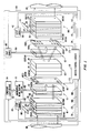
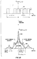
- Commutateur optique comprenant
un réseau (102) d'éléments émetteurs optiques,
un réseau (104) d'éléments récepteurs optiques,
un distributeur optique (103) pour diriger la lumière provenant du réseau d'éléments émetteurs sur le réseau d'éléments récepteurs, où les réseaux sont des réseaux bidimensionnels, les éléments sont disposés en rangées s'étendant dans un sens x et en colonnes s'étendant dans un sens y, et
une source optique (150(1),151(1)) pour diriger la lumière provenant du réseau d'éléments émetteurs sur le réseau d'éléments récepteurs,
CARACTERISE EN CE QUE
les éléments des réseaux sont actionnables sélectivement par rangées,
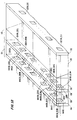
et en ce que le distributeur comprend un moyen de focalisation (501,504,506) ayant des propriétés de focalisation différentes dans les sens x et y, de sorte que les réseaux se trouvent dans des plans conjugués respectifs du distributeur en ce qui concerne la focalisation dans le sens x tandis que le réseau d'éléments récepteurs se trouve dans un plan focal du distributeur en ce qui concerne la focalisation dans le sens y, par lesquelles, en conséquence, la lumière provenant de l'un quelconque des éléments dans l'une quelconque des colonnes du réseau d'éléments émetteurs est distribuée sur tous les éléments dans une colonne correspondante du réseau d'éléments récepteurs, et donc, les informations de n'importe quelle rangée d'éléments émetteurs sont sélectivement transférées à l'une quelconque ou à plusieurs quelconques des rangées d'éléments récepteurs. - Commutateur selon la revendication 1, comportant un système d'entrée optique (101) comprenant une unité de registre de décalage optique (131) disposée pour recevoir des signaux optiques d'une pluralité de voies d'entrée de signaux optiques série (150) pour séparer spatialement les signaux optiques série et un réseau d'éléments de mémorisation d'entrée (132) disposé en rangées et colonnes correspondant à celles du réseau d'éléments émetteurs pour recevoir et mémoriser les signaux séparés spatialement et les appliquer audit réseau d'éléments émetteurs.
- Commutateur selon la revendication 2, dans lequel à chacune des voies d'entrée sont assignées de manière unique une ou plusieurs rangées du réseau d'éléments de mémorisation d'entrée.
- Commutateur selon la revendication 3, dans lequel à une ou plusieurs des voies d'entrée est assignée une pluralité de rangées du réseau d'éléments de mémorisation d'entrée, lesdites rangées correspondant à différentes tranches de temps.
- Commutateur selon l'une quelconque des revendications précédentes, comportant un système optique de sortie (105) comprenant un réseau d'éléments de mémorisation de sortie (133) disposé en rangées et colonnes correspondant à celles du réseau d'éléments récepteurs pour mémoriser les signaux provenant du réseau d'éléments récepteurs et une unité de registre de décalage de sortie (129) disposée pour décaler sériellement les signaux mémorisés dans le réseau d'éléments de mémorisation de sortie en une pluralité de voies de sortie de signaux optiques série (160).
- Commutateur selon la revendication 5, dans lequel à chacune des voies de sortie sont assignées de manière unique une ou plusieurs rangées du réseau d'éléments de mémorisation de sortie.
- Commutateur selon la revendication 6, dans lequel à une ou plusieurs des voies de sortie est assignée une pluralité de rangées du réseau d'éléments de mémorisation de sortie, lesdites rangées correspondant à différentes tranches de temps.
Applications Claiming Priority (2)
| Application Number | Priority Date | Filing Date | Title |
|---|---|---|---|
| US07/140,200 US4830444A (en) | 1987-12-31 | 1987-12-31 | Optical switch |
| US140200 | 1987-12-31 |
Publications (3)
| Publication Number | Publication Date |
|---|---|
| EP0323075A2 EP0323075A2 (fr) | 1989-07-05 |
| EP0323075A3 EP0323075A3 (en) | 1990-07-04 |
| EP0323075B1 true EP0323075B1 (fr) | 1994-03-02 |
Family
ID=22490182
Family Applications (1)
| Application Number | Title | Priority Date | Filing Date |
|---|---|---|---|
| EP88311781A Expired - Lifetime EP0323075B1 (fr) | 1987-12-31 | 1988-12-13 | Commutateur optique |
Country Status (5)
| Country | Link |
|---|---|
| US (1) | US4830444A (fr) |
| EP (1) | EP0323075B1 (fr) |
| JP (1) | JP2816691B2 (fr) |
| CA (1) | CA1292551C (fr) |
| DE (1) | DE3888150T2 (fr) |
Families Citing this family (21)
| Publication number | Priority date | Publication date | Assignee | Title |
|---|---|---|---|---|
| GB8704016D0 (en) * | 1987-02-20 | 1987-04-15 | British Telecomm | Optical space switch |
| US4955686A (en) * | 1989-06-16 | 1990-09-11 | Gte Laboratories Incorporated | Optical fiber crossconnect switch |
| US5093802A (en) * | 1989-06-16 | 1992-03-03 | Rocky Mountain Research Center | Optical computing method using interference fringe component regions |
| US5017986A (en) * | 1989-08-28 | 1991-05-21 | At&T Bell Laboratories | Optical device mounting apparatus |
| US5039182A (en) * | 1989-10-23 | 1991-08-13 | International Business Machines Corporation | Storing information in dual holographic images |
| JPH0821910B2 (ja) * | 1992-03-19 | 1996-03-04 | 日本電気株式会社 | 光メッシュ結合バスインターコネクション |
| US5495356A (en) * | 1993-04-30 | 1996-02-27 | Nec Research Institute, Inc. | Multidimensional switching networks |
| US5644123A (en) * | 1994-12-16 | 1997-07-01 | Rocky Mountain Research Center | Photonic signal processing, amplification, and computing using special interference |
| US5466925A (en) * | 1994-12-16 | 1995-11-14 | Rocky Mountain Research Center | Amplitude to phase conversion logic |
| US5623366A (en) * | 1994-12-16 | 1997-04-22 | Rocky Mountain Research Center | Photonic signal processing amplification, and computing using special interference |
| US5600479A (en) * | 1995-12-22 | 1997-02-04 | Corning Incorporated | Method and apparatus for optical logic and switching functions |
| KR100198782B1 (ko) * | 1996-11-04 | 1999-06-15 | 정선종 | 빔꺽기 소자를 이용한 공간 스위치 |
| US6529305B1 (en) | 1998-11-04 | 2003-03-04 | Corvis Corporation | Optical transmission apparatuses, methods, and systems |
| US6313936B1 (en) * | 2000-09-20 | 2001-11-06 | General Nutronics, Inc. | Method and device for switching wavelength division multiplexed optical signals using micro-electromechanical mirrors |
| US6591033B2 (en) * | 2000-11-06 | 2003-07-08 | Jack Gershfeld | Optical matrix switcher |
| JP2003332560A (ja) * | 2002-05-13 | 2003-11-21 | Semiconductor Energy Lab Co Ltd | 半導体装置及びマイクロプロセッサ |
| US7142743B2 (en) | 2002-05-30 | 2006-11-28 | Corning Incorporated | Latching mechanism for magnetically actuated micro-electro-mechanical devices |
| JP4094386B2 (ja) * | 2002-09-02 | 2008-06-04 | 株式会社半導体エネルギー研究所 | 電子回路装置 |
| JP4373063B2 (ja) | 2002-09-02 | 2009-11-25 | 株式会社半導体エネルギー研究所 | 電子回路装置 |
| JP4574118B2 (ja) * | 2003-02-12 | 2010-11-04 | 株式会社半導体エネルギー研究所 | 半導体装置及びその作製方法 |
| CN1860520B (zh) * | 2003-05-20 | 2011-07-06 | 辛迪安特公司 | 数字底板 |
Family Cites Families (8)
| Publication number | Priority date | Publication date | Assignee | Title |
|---|---|---|---|---|
| FR2489643B1 (fr) * | 1980-09-04 | 1986-12-19 | Rozenwaig Boris | Concentrateur opto-electronique et autocommutateur-concentrateur opto-electronique de liaisons de telecommunications |
| FR2532497B1 (fr) * | 1982-08-24 | 1986-04-18 | Lignes Telegraph Telephon | Dispositif de selection optique et reseau de transmission comportant un tel dispositif |
| US4546244A (en) * | 1984-03-14 | 1985-10-08 | At&T Bell Laboratories | Nonlinear and bistable optical device |
| DE3410629A1 (de) * | 1984-03-22 | 1985-10-03 | Fraunhofer-Gesellschaft zur Förderung der angewandten Forschung e.V., 8000 München | Verfahren und anordnung zum uebertragen von digitalen daten zwischen datenquellen und datensenken |
| US4764890A (en) * | 1984-12-19 | 1988-08-16 | American Telephone And Telegraph Company, At&T Bell Laboratories | Optical logic arrangement |
| US4764889A (en) * | 1984-12-19 | 1988-08-16 | American Telephone And Telegraph Company, At&T Bell Laboratories | Optical logic arrangement with self electro-optic effect devices |
| US4751378B1 (en) * | 1987-04-24 | 2000-04-25 | Bell Telephone Labor Inc | Optical device with quantum well absorption |
| US4754132A (en) * | 1987-04-24 | 1988-06-28 | American Telephone And Telegraph Company, At&T Bell Laboratories | Symmetric optical device with quantum well absorption |
-
1987
- 1987-12-31 US US07/140,200 patent/US4830444A/en not_active Expired - Fee Related
-
1988
- 1988-11-29 CA CA000584410A patent/CA1292551C/fr not_active Expired - Fee Related
- 1988-12-13 EP EP88311781A patent/EP0323075B1/fr not_active Expired - Lifetime
- 1988-12-13 DE DE3888150T patent/DE3888150T2/de not_active Expired - Fee Related
- 1988-12-27 JP JP63328073A patent/JP2816691B2/ja not_active Expired - Lifetime
Also Published As
| Publication number | Publication date |
|---|---|
| DE3888150T2 (de) | 1994-08-25 |
| US4830444A (en) | 1989-05-16 |
| EP0323075A2 (fr) | 1989-07-05 |
| JPH024096A (ja) | 1990-01-09 |
| JP2816691B2 (ja) | 1998-10-27 |
| EP0323075A3 (en) | 1990-07-04 |
| CA1292551C (fr) | 1991-11-26 |
| DE3888150D1 (de) | 1994-04-07 |
Similar Documents
| Publication | Publication Date | Title |
|---|---|---|
| EP0323075B1 (fr) | Commutateur optique | |
| US5953143A (en) | Multidimensional switching networks | |
| Sawchuk et al. | Optical crossbar networks | |
| US3849604A (en) | Time-slot interchanger for time division multiplex system utilizing organ arrays of optical fibers | |
| Kitayama | Novel spatial spread spectrum based fiber optic CDMA networks for image transmission | |
| EP0397372B1 (fr) | Topologie de réseau pour blocage réduit et un système photonique mettant en oeuvre celle-ci | |
| Sawchuk et al. | Geometries for optical implementations of the perfect shuffle | |
| EP0229177B1 (fr) | Agencement de permutation optique | |
| US4917456A (en) | Optical crossover network | |
| EP0397369B1 (fr) | Dispositif optique pour combiner des réseaux lumineux de longueurs d'ondes différentes | |
| US4739520A (en) | Optical switching system | |
| EP0397368B1 (fr) | Procédé de commande d'un réseau de commutation à division spatiale | |
| US5887090A (en) | Optical network | |
| US6473211B2 (en) | Optical crossbar switching and/or routing system | |
| US6259831B1 (en) | All-optical interconnect utilizing polarization gates | |
| CN216310318U (zh) | 一种折叠型m×n端口波长选择开关 | |
| EP0282227A1 (fr) | Processeur de commutation de signal | |
| Yamaguchi et al. | Recent free-space photonic switches | |
| SU1229812A1 (ru) | Устройство дл регистрации электрических сигналов на ленточном оптическом носителе | |
| JP3023221B2 (ja) | 多端子光スイッチ | |
| CN114185135A (zh) | 一种折叠型m×n端口波长选择开关的实现方法 | |
| Hinton | Photonic switching and optical computing based on free-space digital optics | |
| JP3040884B2 (ja) | 光路変換素子 | |
| US20060241500A1 (en) | Method and device for direct ultrahigh speed conversion from time signal to space signal | |
| WO1996001443A1 (fr) | Reseau optique |
Legal Events
| Date | Code | Title | Description |
|---|---|---|---|
| PUAI | Public reference made under article 153(3) epc to a published international application that has entered the european phase |
Free format text: ORIGINAL CODE: 0009012 |
|
| AK | Designated contracting states |
Kind code of ref document: A2 Designated state(s): BE DE ES FR GB IT NL SE |
|
| PUAL | Search report despatched |
Free format text: ORIGINAL CODE: 0009013 |
|
| AK | Designated contracting states |
Kind code of ref document: A3 Designated state(s): BE DE ES FR GB IT NL SE |
|
| 17P | Request for examination filed |
Effective date: 19901206 |
|
| 17Q | First examination report despatched |
Effective date: 19921014 |
|
| GRAA | (expected) grant |
Free format text: ORIGINAL CODE: 0009210 |
|
| AK | Designated contracting states |
Kind code of ref document: B1 Designated state(s): BE DE ES FR GB IT NL SE |
|
| PG25 | Lapsed in a contracting state [announced via postgrant information from national office to epo] |
Ref country code: IT Free format text: LAPSE BECAUSE OF FAILURE TO SUBMIT A TRANSLATION OF THE DESCRIPTION OR TO PAY THE FEE WITHIN THE PRE;WARNING: LAPSES OF ITALIAN PATENTS WITH EFFECTIVE DATE BEFORE 2007 MAY HAVE OCCURRED AT ANY TIME BEFORE 2007. THE CORRECT EFFECTIVE DATE MAY BE DIFFERENT FROM THE ONE RECORDED.SCRIBED TIME-LIMIT Effective date: 19940302 Ref country code: SE Free format text: THE PATENT HAS BEEN ANNULLED BY A DECISION OF A NATIONAL AUTHORITY Effective date: 19940302 Ref country code: NL Effective date: 19940302 Ref country code: ES Free format text: THE PATENT HAS BEEN ANNULLED BY A DECISION OF A NATIONAL AUTHORITY Effective date: 19940302 Ref country code: BE Effective date: 19940302 |
|
| ET | Fr: translation filed | ||
| REF | Corresponds to: |
Ref document number: 3888150 Country of ref document: DE Date of ref document: 19940407 |
|
| RAP4 | Party data changed (patent owner data changed or rights of a patent transferred) |
Owner name: AT&T CORP. |
|
| NLV1 | Nl: lapsed or annulled due to failure to fulfill the requirements of art. 29p and 29m of the patents act | ||
| PLBE | No opposition filed within time limit |
Free format text: ORIGINAL CODE: 0009261 |
|
| STAA | Information on the status of an ep patent application or granted ep patent |
Free format text: STATUS: NO OPPOSITION FILED WITHIN TIME LIMIT |
|
| 26N | No opposition filed | ||
| PGFP | Annual fee paid to national office [announced via postgrant information from national office to epo] |
Ref country code: FR Payment date: 19991124 Year of fee payment: 12 |
|
| PGFP | Annual fee paid to national office [announced via postgrant information from national office to epo] |
Ref country code: GB Payment date: 19991126 Year of fee payment: 12 |
|
| PGFP | Annual fee paid to national office [announced via postgrant information from national office to epo] |
Ref country code: DE Payment date: 19991231 Year of fee payment: 12 |
|
| PG25 | Lapsed in a contracting state [announced via postgrant information from national office to epo] |
Ref country code: GB Free format text: LAPSE BECAUSE OF NON-PAYMENT OF DUE FEES Effective date: 20001213 |
|
| GBPC | Gb: european patent ceased through non-payment of renewal fee |
Effective date: 20001213 |
|
| PG25 | Lapsed in a contracting state [announced via postgrant information from national office to epo] |
Ref country code: FR Free format text: LAPSE BECAUSE OF NON-PAYMENT OF DUE FEES Effective date: 20010831 |
|
| REG | Reference to a national code |
Ref country code: FR Ref legal event code: ST |
|
| PG25 | Lapsed in a contracting state [announced via postgrant information from national office to epo] |
Ref country code: DE Free format text: LAPSE BECAUSE OF NON-PAYMENT OF DUE FEES Effective date: 20011002 |