EP0323075B1 - Optische Vermittlung - Google Patents
Optische Vermittlung Download PDFInfo
- Publication number
- EP0323075B1 EP0323075B1 EP88311781A EP88311781A EP0323075B1 EP 0323075 B1 EP0323075 B1 EP 0323075B1 EP 88311781 A EP88311781 A EP 88311781A EP 88311781 A EP88311781 A EP 88311781A EP 0323075 B1 EP0323075 B1 EP 0323075B1
- Authority
- EP
- European Patent Office
- Prior art keywords
- array
- optical
- output
- input
- rows
- Prior art date
- Legal status (The legal status is an assumption and is not a legal conclusion. Google has not performed a legal analysis and makes no representation as to the accuracy of the status listed.)
- Expired - Lifetime
Links
Images


Classifications
-
- H—ELECTRICITY
- H04—ELECTRIC COMMUNICATION TECHNIQUE
- H04Q—SELECTING
- H04Q11/00—Selecting arrangements for multiplex systems
- H04Q11/0001—Selecting arrangements for multiplex systems using optical switching
- H04Q11/0003—Details
Landscapes
- Engineering & Computer Science (AREA)
- Computer Networks & Wireless Communication (AREA)
- Use Of Switch Circuits For Exchanges And Methods Of Control Of Multiplex Exchanges (AREA)
- Optical Communication System (AREA)
Claims (7)
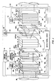
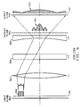
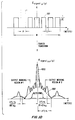
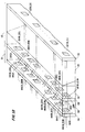
- Optischer Koppelnetzbaustein mit einem Feld (102) optischer Senderelemente, einem Feld (104) optischer Empfängerelemente, einem optischen Verteiler (103) zum Leiten von Licht von dem Feld von Senderelementen zum Feld von Empfängerelementen, wobei die Felder zweidimensionale Felder sind, die Elemente in sich in einer X-Richtung erstreckenden Zeilen und sich in einer Y-Richtung erstreckenden Spalten angeordnet sind, und einer optischen Quelle (150(1), 151(1)) zum Leiten von Licht von dem Feld von Senderelementen zum Feld von Empfängerelementen, dadurch gekennzeichnet, daß die Elemente der Felder gezielt zeilenweise ansteuerbar sind, und daß der Verteiler Fokussiermittel (501, 504, 506) mit unterschiedlichen Fokussiereigenschaften in den X- und Y-Richtungen umfaßt, so daß die Felder in bezug auf die Fokussierung in der X-Richtung in entsprechenden zugeordneten Ebenen des Verteilers liegen, während das Feld von Empfängerelementen in bezug auf die Fokussierung in der Y-Richtung in einer Fokalebene des Verteilers liegt, wodurch als Ergebnis Licht von einem beliebigen der Elemente in einer beliebigen der Spalten des Feldes von Senderelementen über alle Elemente in einer entsprechenden Spalte des Feldes von Empfängerelementen verteilt wird und auf diese Weise die Information von einer beliebigen Zeile von Senderelementen gezielt zu einer oder mehr als einer beliebigen der Zeilen von Empfängerelementen übertragen wird.
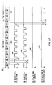
- Koppelnetzbaustein nach Anspruch 1, mit einem optischen Eingabesystem (101) mit einer optischen Schieberegistereinheit (131), die zum Empfang von optischen Signalen von einer Mehrzahl von seriellen optischen Signaleingangskanälen (150) zum räumlichen Trennen der seriellen optischen Signale angeordnet ist, und einem Eingangsspeicherelementfeld (132), das in Zeilen und Spalten entsprechend denen des Feldes von Senderelementen für den Empfang und die Speicherung der räumlich getrennten Signale und zum Anlegen derselben an das besagte Feld von Senderelementen angeordnet ist.
- Koppelnetzbaustein nach Anspruch 2, dadurch gekennzeichnet, daß jedem der Eingangskanäle eindeutig eine oder mehrere Zeilen des Eingangsspeicherelementfeldes zugewiesen ist.
- Koppelnetzbaustein nach Anspruch 3, dadurch gekennzeichnet, daß einem oder mehreren der Eingangskanäle eine Mehrzahl von Zeilen des Eingangsspeicherfeldes zugewiesen ist, wobei die besagten Zeilen unterschiedlichen Zeitschlitzen entsprechen.
- Koppelnetzbaustein nach einem beliebigen der vorhergehenden Ansprüche, mit einem optischen Ausgangssystem (105) mit einem Ausgangsspeicherelementfeld (133), das in Zeilen und Spalten entsprechend denen des Feldes von Empfängerelementen zur Speicherung von Signalen von dem Feld von Empfängerelementen angeordnet ist, und einer Ausgangsschieberegistereinheit (129), die zum seriellen Verschieben von in dem Ausgangsspeicherelementfeld gespeicherten Signalen in eine Mehrzahl von seriellen optischen Signalausgangskanälen (160) angeordnet ist.
- Koppelnetzbaustein nach Anspruch 5, dadurch gekennzeichnet, daß jedem der Ausgangskanäle eindeutig eine oder mehrere Zeilen des Ausgangsspeicherelementfeldes zugewiesen ist.
- Koppelnetzbaustein nach Anspruch 6, dadurch gekennzeichnet, daß einem oder mehreren der Ausgangskanäle eine Mehrzahl von Zeilen des Ausgangsspeicherelementfeldes zugewiesen ist, wobei die besagten Zeilen unterschiedlichen Zeitschlitzen entsprechen.
Applications Claiming Priority (2)
| Application Number | Priority Date | Filing Date | Title |
|---|---|---|---|
| US07/140,200 US4830444A (en) | 1987-12-31 | 1987-12-31 | Optical switch |
| US140200 | 1987-12-31 |
Publications (3)
| Publication Number | Publication Date |
|---|---|
| EP0323075A2 EP0323075A2 (de) | 1989-07-05 |
| EP0323075A3 EP0323075A3 (en) | 1990-07-04 |
| EP0323075B1 true EP0323075B1 (de) | 1994-03-02 |
Family
ID=22490182
Family Applications (1)
| Application Number | Title | Priority Date | Filing Date |
|---|---|---|---|
| EP88311781A Expired - Lifetime EP0323075B1 (de) | 1987-12-31 | 1988-12-13 | Optische Vermittlung |
Country Status (5)
| Country | Link |
|---|---|
| US (1) | US4830444A (de) |
| EP (1) | EP0323075B1 (de) |
| JP (1) | JP2816691B2 (de) |
| CA (1) | CA1292551C (de) |
| DE (1) | DE3888150T2 (de) |
Families Citing this family (21)
| Publication number | Priority date | Publication date | Assignee | Title |
|---|---|---|---|---|
| GB8704016D0 (en) * | 1987-02-20 | 1987-04-15 | British Telecomm | Optical space switch |
| US4955686A (en) * | 1989-06-16 | 1990-09-11 | Gte Laboratories Incorporated | Optical fiber crossconnect switch |
| US5093802A (en) * | 1989-06-16 | 1992-03-03 | Rocky Mountain Research Center | Optical computing method using interference fringe component regions |
| US5017986A (en) * | 1989-08-28 | 1991-05-21 | At&T Bell Laboratories | Optical device mounting apparatus |
| US5039182A (en) * | 1989-10-23 | 1991-08-13 | International Business Machines Corporation | Storing information in dual holographic images |
| JPH0821910B2 (ja) * | 1992-03-19 | 1996-03-04 | 日本電気株式会社 | 光メッシュ結合バスインターコネクション |
| US5495356A (en) * | 1993-04-30 | 1996-02-27 | Nec Research Institute, Inc. | Multidimensional switching networks |
| US5644123A (en) * | 1994-12-16 | 1997-07-01 | Rocky Mountain Research Center | Photonic signal processing, amplification, and computing using special interference |
| US5466925A (en) * | 1994-12-16 | 1995-11-14 | Rocky Mountain Research Center | Amplitude to phase conversion logic |
| US5623366A (en) * | 1994-12-16 | 1997-04-22 | Rocky Mountain Research Center | Photonic signal processing amplification, and computing using special interference |
| US5600479A (en) * | 1995-12-22 | 1997-02-04 | Corning Incorporated | Method and apparatus for optical logic and switching functions |
| KR100198782B1 (ko) * | 1996-11-04 | 1999-06-15 | 정선종 | 빔꺽기 소자를 이용한 공간 스위치 |
| US6529305B1 (en) | 1998-11-04 | 2003-03-04 | Corvis Corporation | Optical transmission apparatuses, methods, and systems |
| US6313936B1 (en) * | 2000-09-20 | 2001-11-06 | General Nutronics, Inc. | Method and device for switching wavelength division multiplexed optical signals using micro-electromechanical mirrors |
| US6591033B2 (en) * | 2000-11-06 | 2003-07-08 | Jack Gershfeld | Optical matrix switcher |
| JP2003332560A (ja) * | 2002-05-13 | 2003-11-21 | Semiconductor Energy Lab Co Ltd | 半導体装置及びマイクロプロセッサ |
| US7142743B2 (en) | 2002-05-30 | 2006-11-28 | Corning Incorporated | Latching mechanism for magnetically actuated micro-electro-mechanical devices |
| JP4094386B2 (ja) * | 2002-09-02 | 2008-06-04 | 株式会社半導体エネルギー研究所 | 電子回路装置 |
| JP4373063B2 (ja) | 2002-09-02 | 2009-11-25 | 株式会社半導体エネルギー研究所 | 電子回路装置 |
| JP4574118B2 (ja) * | 2003-02-12 | 2010-11-04 | 株式会社半導体エネルギー研究所 | 半導体装置及びその作製方法 |
| CN1860520B (zh) * | 2003-05-20 | 2011-07-06 | 辛迪安特公司 | 数字底板 |
Family Cites Families (8)
| Publication number | Priority date | Publication date | Assignee | Title |
|---|---|---|---|---|
| FR2489643B1 (fr) * | 1980-09-04 | 1986-12-19 | Rozenwaig Boris | Concentrateur opto-electronique et autocommutateur-concentrateur opto-electronique de liaisons de telecommunications |
| FR2532497B1 (fr) * | 1982-08-24 | 1986-04-18 | Lignes Telegraph Telephon | Dispositif de selection optique et reseau de transmission comportant un tel dispositif |
| US4546244A (en) * | 1984-03-14 | 1985-10-08 | At&T Bell Laboratories | Nonlinear and bistable optical device |
| DE3410629A1 (de) * | 1984-03-22 | 1985-10-03 | Fraunhofer-Gesellschaft zur Förderung der angewandten Forschung e.V., 8000 München | Verfahren und anordnung zum uebertragen von digitalen daten zwischen datenquellen und datensenken |
| US4764890A (en) * | 1984-12-19 | 1988-08-16 | American Telephone And Telegraph Company, At&T Bell Laboratories | Optical logic arrangement |
| US4764889A (en) * | 1984-12-19 | 1988-08-16 | American Telephone And Telegraph Company, At&T Bell Laboratories | Optical logic arrangement with self electro-optic effect devices |
| US4751378B1 (en) * | 1987-04-24 | 2000-04-25 | Bell Telephone Labor Inc | Optical device with quantum well absorption |
| US4754132A (en) * | 1987-04-24 | 1988-06-28 | American Telephone And Telegraph Company, At&T Bell Laboratories | Symmetric optical device with quantum well absorption |
-
1987
- 1987-12-31 US US07/140,200 patent/US4830444A/en not_active Expired - Fee Related
-
1988
- 1988-11-29 CA CA000584410A patent/CA1292551C/en not_active Expired - Fee Related
- 1988-12-13 EP EP88311781A patent/EP0323075B1/de not_active Expired - Lifetime
- 1988-12-13 DE DE3888150T patent/DE3888150T2/de not_active Expired - Fee Related
- 1988-12-27 JP JP63328073A patent/JP2816691B2/ja not_active Expired - Lifetime
Also Published As
| Publication number | Publication date |
|---|---|
| DE3888150T2 (de) | 1994-08-25 |
| US4830444A (en) | 1989-05-16 |
| EP0323075A2 (de) | 1989-07-05 |
| JPH024096A (ja) | 1990-01-09 |
| JP2816691B2 (ja) | 1998-10-27 |
| EP0323075A3 (en) | 1990-07-04 |
| CA1292551C (en) | 1991-11-26 |
| DE3888150D1 (de) | 1994-04-07 |
Similar Documents
| Publication | Publication Date | Title |
|---|---|---|
| EP0323075B1 (de) | Optische Vermittlung | |
| US5953143A (en) | Multidimensional switching networks | |
| Sawchuk et al. | Optical crossbar networks | |
| US3849604A (en) | Time-slot interchanger for time division multiplex system utilizing organ arrays of optical fibers | |
| Kitayama | Novel spatial spread spectrum based fiber optic CDMA networks for image transmission | |
| EP0397372B1 (de) | Netztopologie für reduzierte Blockierung und entsprechende photonische Systemausführung | |
| Sawchuk et al. | Geometries for optical implementations of the perfect shuffle | |
| EP0229177B1 (de) | Optische umordnungsanordnung | |
| US4917456A (en) | Optical crossover network | |
| EP0397369B1 (de) | Optische Vorrichtung zum Kombinieren von Lichtstrahlen-Matrizen mit verschiedenen Wellenlängen | |
| US4739520A (en) | Optical switching system | |
| EP0397368B1 (de) | Steuerungsverfahren für Raumvielfachkoppelnetz | |
| US5887090A (en) | Optical network | |
| US6473211B2 (en) | Optical crossbar switching and/or routing system | |
| US6259831B1 (en) | All-optical interconnect utilizing polarization gates | |
| CN216310318U (zh) | 一种折叠型m×n端口波长选择开关 | |
| EP0282227A1 (de) | Signalschaltprozessor | |
| Yamaguchi et al. | Recent free-space photonic switches | |
| SU1229812A1 (ru) | Устройство дл регистрации электрических сигналов на ленточном оптическом носителе | |
| JP3023221B2 (ja) | 多端子光スイッチ | |
| CN114185135A (zh) | 一种折叠型m×n端口波长选择开关的实现方法 | |
| Hinton | Photonic switching and optical computing based on free-space digital optics | |
| JP3040884B2 (ja) | 光路変換素子 | |
| US20060241500A1 (en) | Method and device for direct ultrahigh speed conversion from time signal to space signal | |
| WO1996001443A1 (en) | An optical network |
Legal Events
| Date | Code | Title | Description |
|---|---|---|---|
| PUAI | Public reference made under article 153(3) epc to a published international application that has entered the european phase |
Free format text: ORIGINAL CODE: 0009012 |
|
| AK | Designated contracting states |
Kind code of ref document: A2 Designated state(s): BE DE ES FR GB IT NL SE |
|
| PUAL | Search report despatched |
Free format text: ORIGINAL CODE: 0009013 |
|
| AK | Designated contracting states |
Kind code of ref document: A3 Designated state(s): BE DE ES FR GB IT NL SE |
|
| 17P | Request for examination filed |
Effective date: 19901206 |
|
| 17Q | First examination report despatched |
Effective date: 19921014 |
|
| GRAA | (expected) grant |
Free format text: ORIGINAL CODE: 0009210 |
|
| AK | Designated contracting states |
Kind code of ref document: B1 Designated state(s): BE DE ES FR GB IT NL SE |
|
| PG25 | Lapsed in a contracting state [announced via postgrant information from national office to epo] |
Ref country code: IT Free format text: LAPSE BECAUSE OF FAILURE TO SUBMIT A TRANSLATION OF THE DESCRIPTION OR TO PAY THE FEE WITHIN THE PRE;WARNING: LAPSES OF ITALIAN PATENTS WITH EFFECTIVE DATE BEFORE 2007 MAY HAVE OCCURRED AT ANY TIME BEFORE 2007. THE CORRECT EFFECTIVE DATE MAY BE DIFFERENT FROM THE ONE RECORDED.SCRIBED TIME-LIMIT Effective date: 19940302 Ref country code: SE Free format text: THE PATENT HAS BEEN ANNULLED BY A DECISION OF A NATIONAL AUTHORITY Effective date: 19940302 Ref country code: NL Effective date: 19940302 Ref country code: ES Free format text: THE PATENT HAS BEEN ANNULLED BY A DECISION OF A NATIONAL AUTHORITY Effective date: 19940302 Ref country code: BE Effective date: 19940302 |
|
| ET | Fr: translation filed | ||
| REF | Corresponds to: |
Ref document number: 3888150 Country of ref document: DE Date of ref document: 19940407 |
|
| RAP4 | Party data changed (patent owner data changed or rights of a patent transferred) |
Owner name: AT&T CORP. |
|
| NLV1 | Nl: lapsed or annulled due to failure to fulfill the requirements of art. 29p and 29m of the patents act | ||
| PLBE | No opposition filed within time limit |
Free format text: ORIGINAL CODE: 0009261 |
|
| STAA | Information on the status of an ep patent application or granted ep patent |
Free format text: STATUS: NO OPPOSITION FILED WITHIN TIME LIMIT |
|
| 26N | No opposition filed | ||
| PGFP | Annual fee paid to national office [announced via postgrant information from national office to epo] |
Ref country code: FR Payment date: 19991124 Year of fee payment: 12 |
|
| PGFP | Annual fee paid to national office [announced via postgrant information from national office to epo] |
Ref country code: GB Payment date: 19991126 Year of fee payment: 12 |
|
| PGFP | Annual fee paid to national office [announced via postgrant information from national office to epo] |
Ref country code: DE Payment date: 19991231 Year of fee payment: 12 |
|
| PG25 | Lapsed in a contracting state [announced via postgrant information from national office to epo] |
Ref country code: GB Free format text: LAPSE BECAUSE OF NON-PAYMENT OF DUE FEES Effective date: 20001213 |
|
| GBPC | Gb: european patent ceased through non-payment of renewal fee |
Effective date: 20001213 |
|
| PG25 | Lapsed in a contracting state [announced via postgrant information from national office to epo] |
Ref country code: FR Free format text: LAPSE BECAUSE OF NON-PAYMENT OF DUE FEES Effective date: 20010831 |
|
| REG | Reference to a national code |
Ref country code: FR Ref legal event code: ST |
|
| PG25 | Lapsed in a contracting state [announced via postgrant information from national office to epo] |
Ref country code: DE Free format text: LAPSE BECAUSE OF NON-PAYMENT OF DUE FEES Effective date: 20011002 |