EP0322962A1 - Circuit intégré présentant un transistor latéral - Google Patents
Circuit intégré présentant un transistor latéral Download PDFInfo
- Publication number
- EP0322962A1 EP0322962A1 EP88202929A EP88202929A EP0322962A1 EP 0322962 A1 EP0322962 A1 EP 0322962A1 EP 88202929 A EP88202929 A EP 88202929A EP 88202929 A EP88202929 A EP 88202929A EP 0322962 A1 EP0322962 A1 EP 0322962A1
- Authority
- EP
- European Patent Office
- Prior art keywords
- emitter
- region
- integrated circuit
- emitter region
- circuit according
- Prior art date
- Legal status (The legal status is an assumption and is not a legal conclusion. Google has not performed a legal analysis and makes no representation as to the accuracy of the status listed.)
- Granted
Links
- 239000000969 carrier Substances 0.000 claims abstract description 7
- 238000009792 diffusion process Methods 0.000 claims abstract description 4
- 239000010432 diamond Substances 0.000 claims description 9
- 229910003460 diamond Inorganic materials 0.000 claims description 3
- 238000002347 injection Methods 0.000 description 9
- 239000007924 injection Substances 0.000 description 9
- 239000000758 substrate Substances 0.000 description 3
- 238000000034 method Methods 0.000 description 2
- 238000004519 manufacturing process Methods 0.000 description 1
- 238000005457 optimization Methods 0.000 description 1
Images

Classifications
-
- H—ELECTRICITY
- H01—ELECTRIC ELEMENTS
- H01L—SEMICONDUCTOR DEVICES NOT COVERED BY CLASS H10
- H01L29/00—Semiconductor devices adapted for rectifying, amplifying, oscillating or switching, or capacitors or resistors with at least one potential-jump barrier or surface barrier, e.g. PN junction depletion layer or carrier concentration layer; Details of semiconductor bodies or of electrodes thereof ; Multistep manufacturing processes therefor
- H01L29/66—Types of semiconductor device ; Multistep manufacturing processes therefor
- H01L29/68—Types of semiconductor device ; Multistep manufacturing processes therefor controllable by only the electric current supplied, or only the electric potential applied, to an electrode which does not carry the current to be rectified, amplified or switched
-
- H—ELECTRICITY
- H01—ELECTRIC ELEMENTS
- H01L—SEMICONDUCTOR DEVICES NOT COVERED BY CLASS H10
- H01L29/00—Semiconductor devices adapted for rectifying, amplifying, oscillating or switching, or capacitors or resistors with at least one potential-jump barrier or surface barrier, e.g. PN junction depletion layer or carrier concentration layer; Details of semiconductor bodies or of electrodes thereof ; Multistep manufacturing processes therefor
- H01L29/02—Semiconductor bodies ; Multistep manufacturing processes therefor
- H01L29/06—Semiconductor bodies ; Multistep manufacturing processes therefor characterised by their shape; characterised by the shapes, relative sizes, or dispositions of the semiconductor regions ; characterised by the concentration or distribution of impurities within semiconductor regions
- H01L29/0684—Semiconductor bodies ; Multistep manufacturing processes therefor characterised by their shape; characterised by the shapes, relative sizes, or dispositions of the semiconductor regions ; characterised by the concentration or distribution of impurities within semiconductor regions characterised by the shape, relative sizes or dispositions of the semiconductor regions or junctions between the regions
- H01L29/0692—Surface layout
-
- H—ELECTRICITY
- H01—ELECTRIC ELEMENTS
- H01L—SEMICONDUCTOR DEVICES NOT COVERED BY CLASS H10
- H01L29/00—Semiconductor devices adapted for rectifying, amplifying, oscillating or switching, or capacitors or resistors with at least one potential-jump barrier or surface barrier, e.g. PN junction depletion layer or carrier concentration layer; Details of semiconductor bodies or of electrodes thereof ; Multistep manufacturing processes therefor
- H01L29/02—Semiconductor bodies ; Multistep manufacturing processes therefor
- H01L29/06—Semiconductor bodies ; Multistep manufacturing processes therefor characterised by their shape; characterised by the shapes, relative sizes, or dispositions of the semiconductor regions ; characterised by the concentration or distribution of impurities within semiconductor regions
- H01L29/08—Semiconductor bodies ; Multistep manufacturing processes therefor characterised by their shape; characterised by the shapes, relative sizes, or dispositions of the semiconductor regions ; characterised by the concentration or distribution of impurities within semiconductor regions with semiconductor regions connected to an electrode carrying current to be rectified, amplified or switched and such electrode being part of a semiconductor device which comprises three or more electrodes
-
- H—ELECTRICITY
- H01—ELECTRIC ELEMENTS
- H01L—SEMICONDUCTOR DEVICES NOT COVERED BY CLASS H10
- H01L29/00—Semiconductor devices adapted for rectifying, amplifying, oscillating or switching, or capacitors or resistors with at least one potential-jump barrier or surface barrier, e.g. PN junction depletion layer or carrier concentration layer; Details of semiconductor bodies or of electrodes thereof ; Multistep manufacturing processes therefor
- H01L29/40—Electrodes ; Multistep manufacturing processes therefor
- H01L29/41—Electrodes ; Multistep manufacturing processes therefor characterised by their shape, relative sizes or dispositions
- H01L29/417—Electrodes ; Multistep manufacturing processes therefor characterised by their shape, relative sizes or dispositions carrying the current to be rectified, amplified or switched
- H01L29/41708—Emitter or collector electrodes for bipolar transistors
-
- H—ELECTRICITY
- H01—ELECTRIC ELEMENTS
- H01L—SEMICONDUCTOR DEVICES NOT COVERED BY CLASS H10
- H01L29/00—Semiconductor devices adapted for rectifying, amplifying, oscillating or switching, or capacitors or resistors with at least one potential-jump barrier or surface barrier, e.g. PN junction depletion layer or carrier concentration layer; Details of semiconductor bodies or of electrodes thereof ; Multistep manufacturing processes therefor
- H01L29/66—Types of semiconductor device ; Multistep manufacturing processes therefor
- H01L29/68—Types of semiconductor device ; Multistep manufacturing processes therefor controllable by only the electric current supplied, or only the electric potential applied, to an electrode which does not carry the current to be rectified, amplified or switched
- H01L29/70—Bipolar devices
- H01L29/72—Transistor-type devices, i.e. able to continuously respond to applied control signals
- H01L29/73—Bipolar junction transistors
- H01L29/735—Lateral transistors
Definitions
- the present invention relates to an integrated circuit having a lateral transistor comprising emitter and collector regions of a first type of conductivity spaced apart laterally and arranged from the surface of a region of a second type of opposite conductivity in the first, the lateral space of said region of the second type located between the emitter and collector regions forming the base of the transistor, and comprising electrical emitter and collector connections, each of which has at least one region in electrical contact through windows of an insulating layer respectively with said emitter region and with said collector region, the emitter region having a depth and a doping level such as the diffusion length of the minority carriers vertically injected therein ci is greater than or equal to the thickness of said region, and the ratio between the area of said emitter region and that of said area of electric transmitter harness being at least equal to 20.
- the lateral transistor as described in this prior art has an improved gain by a factor of up to approximately 1.4 compared to the lateral transistors produced previously.
- the subject of the present invention is an internal circuit with a lateral transistor whose current gain is close to that of the vertical transistors, for example a gain of the order of 40.
- the basic idea of the invention consists in breaking with the principle of symmetry governing the geometry of the emitters of the lateral transistors. According to this principle, the emitter contact is not far from the emitter-base junction, which is supposed to improve the efficiency of the lateral injection.
- the Applicant has been able to demonstrate that, surprisingly, it was possible to obtain a remarkably high current gain with a geometry in which a significant part of the emitter-base junction was very far from the emitter contact, according to at least a preferential direction.
- the integrated circuit according to the invention is thus characterized in that the emitter region has at least one elongated branch in a first so-called longitudinal direction, the ratio between the largest dimension along said longitudinal dimension and the greatest width of said branch transverse being at least equal to 5.
- the emitter region is diamond-shaped.
- the emitter region has at least one strip, for example in the form of diamonds connected according to the longitudinal dimension, and a plurality of contact pads.
- the emitter region comprises at least two branches in at least a first and a second so-called longitudinal directions.
- the emitter region may have at least two bands in at least said first and second said longitudinal directions, each band having a plurality of contact pads.
- at least one collector island can be arranged in the space existing between the bands.
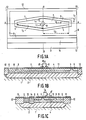
- a lateral transistor according to the invention comprises an emitter region 7 of elongated shape, here in the form of a truncated diamond shape at the center of which is an opening 8 of a thin oxide layer 11, and used for contacting the transmitter.
- the integrated circuit comprises a substrate 1, for example of the p type, in a region of which a buried layer 2 is heavily doped of the opposite type, therefore n+.
- the substrate 1 is covered with an epitaxial layer of opposite type, therefore n, having localized wells, here 4 and 3, respectively forming a well for the lateral transistor and a basic contact well electrically connected to each other. another by the heavily doped buried layer 2.
- the box 3 has a generally rectangular shape and is separated from the box 4 by a deep oxide region 14 which extends to the buried layer 2.
- the box 4 is also of rectangular dimension and is bordered on three sides by a deep oxide region 12 which extends to the buried layer 2, and on the fourth side by the deep oxide region 14.
- the box 3 is bordered on its three non-adjacent sides of the box 4 by the region of deep oxide 12 which thus borders all of the two boxes 3 and 4.
- the box 4 has regions here of type p, forming the emitter 7 and collector regions 6.
- the collector region 6 is bordered externally by the deep oxide layers 12 and 14.
- the base region 5 is constituted by the n-type region of well 4 which remains between regions 6 and 7.
- the opening 8 is, in this case, of square section and its diagonals are arranged along the axes of the rhombus constituting the transmitter 7.
- a contact pad 8 ′ shown in FIGS. 1b and 1c allows contact to be made transmitter.
- the side of the opening 8 has the value L1 and its diagonal 2L5 is the value L1 ⁇ 2.
- L2 be the value of the main half-diagonal of the rhombus and L4 + L5 the value of the other half-diagonal of the rhombus.
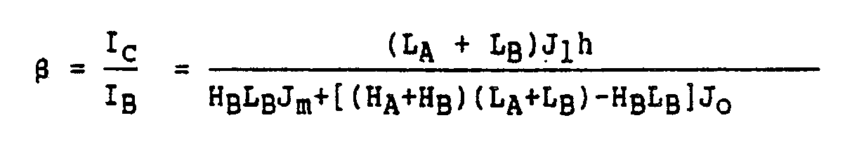
- the emitter region 7 has a depth h and a doping level such that the diffusion length of the minority carriers vertically injected into it is greater than or equal to the thickness of this region.
- J1 the lateral injection current density of minority carriers in base 5
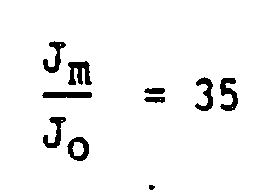
- J m the vertical injection current density of minority carriers under the emitter contact area (8)
- J0 la vertical injection current density of minority carriers under the portion of the oxide layer 11 which covers the emitter region 7.
- the value of the gain constantly increases when the ratio between the emitter contact surface and the surface of the emitter region increases. This result is quite surprising for two reasons. On the one hand, it highlights a particular case where the value of the gain does not go through a maximum contrary to the teaching of the aforementioned French patent application 85 19479, and on the other hand the maximum value of the gain ⁇ M is several times higher than that obtained from the above-mentioned request.
- the gain of the transistor is practically only the consequence of the lateral injection induced by the injection under the oxide, this injection under oxide being itself the consequence of the injection under the contact region d 'transmitter. It is precisely the elongated shape of the transmitter in a preferred direction which makes it possible to take full advantage of this phenomenon of injection under the oxide, which was generally perceived as being an undesirable phenomenon.
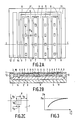
- the transmitter 7 comprises a plurality of bands 7, each band comprising a transmitter contact band forming a plurality of contacts through openings 8.
- the contact pads 8 ′ (not shown) are interconnected by conductive strips themselves interconnected.
- the other substrate elements 1, buried layer 2, wells 3 and 4, etc. have the same reference numbers as in FIGS. 1a to 1c.
- this band structure manifests itself (see section CC of FIG. 2b), by a succession of bands of emitter 7 and collector regions 6 separated by bands of base region 5.
- the collector region strips 6 are interconnected by sections 6 ′.
- the current gain is limited by the emitter resistance induced in the case of FIGS. 1a to 1c, by the length of the emitter, and in the case of FIGS. 2a and 2b, by the spacing between the regions. contact transmitter.
- the emitter resistance tends to lower the maximum admissible current, the current gain starting to drop from a certain level of current. It is therefore necessary to choose in the first case the length of the diamonds and in the second case the spacing between the emitter contacts so as to reconcile a high gain with an acceptable emitter resistance.
- the structure which comprises several bands in parallel makes it possible to multiply the maximum current of the transistor. This structure is therefore particularly advantageous and generally makes it possible to obtain a better optimization than a single-band structure.
- a structure comprising a single emitter band is advantageous for operations at low or very low currents for which only the current gain of the transistor is of importance.
- FIG. 4 represents a variant of the invention, in which the transmitter comprises a strip formed by two truncated diamonds connected together.
- Figures 5a and 5b show another variant of the invention in which the transmitter comprises two bands each consisting of several truncated diamonds connected together, here three in number per band.
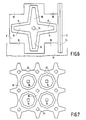
- the transmitter comprises two branches 15 and 16 arranged in two so-called longitudinal directions, at the intersection of which is disposed a transmitter contact 24.
- the two branches 15 and 16 are shown here as two orthogonal diamonds with the same center.
- the perimeter of the emitter is surrounded by the base region 5 itself surrounded by the collector region 6, which comprises an emitter contacting area 19.
- a layer 14 d 'deep oxide separates the box 3 used for making basic contact.
- This structure with two (or more) branches makes it possible to limit the bulk while allowing a reduced emitter resistance, which makes it possible to maintain the high value of the gain at higher currents.
- This arrangement according to several dimensions also has the advantage of being suitable for a checkerboard embodiment, in two or more directions, making it possible to increase the possibilities in current, therefore in power.
- FIG. 7 An embodiment is represented in FIG. 7 according to which elementary structures with two branches according to FIG. 6 are assembled by the end of the branches, constituting in their turn strips arranged in the two longitudinal directions. When there are at least four such strips, at least one collector island can be arranged in the space existing between the strips. In Figure 7, six bands and four islands have been shown. Each island has a collector contact 19.
Abstract
Description
- La présente invention a pour objet un circuit intégré présentant un transistor latéral comportant des régions d'émetteur et de collecteur d'un premier type de conductivité espacées latéralement et disposées à partir de la surface d'une région d'un deuxième type de conductivité opposé au premier, l'espace latéral de ladite région du deuxième type situé entre les régions d'émetteur et de collecteur formant la base du transistor, et comportant des liaisons électriques d'émetteur et de collecteur dont chacune présente au moins une zone en contact électrique à travers des fenêtres d'une couche isolante respectivement avec ladite région d'émetteur et avec ladite région de collecteur, la région d'émetteur présentant une profondeur et un niveau de dopage tels que la longueur de diffusion des porteurs minoritaires injectés verticalement dans celle-ci est supérieure ou égale à l'épaisseur de ladite région, et le rapport entre la surface de ladite région d'émetteur et celle de ladite zone de laison électrique d'émetteur étant au moins égal à 20.
- Un tel circuit a été décrit dans la demande de brevet français n° 85 19479 déposée le 31 décembre 1985 par la Demanderesse et intitublée "Procédé de fabrication d'un transistor latéral intégré et circuit intégré le comprenant".
- Le transistor latéral tel que décrit dans cette antériorité présente un gain amélioré d'un facteur pouvant atteindre environ 1,4 par rapport aux transistors latéraux réalisés auparavant.
- On peut ainsi obtenir des transistors latéraux dont le gain en courant est de l'ordre de 10.
- Cependant, un des problèmes cruciaux que posent les transistors latéraux est que leur gain en courant reste très inférieur aux gains en courant des transistors verticaux, qui peuvent être de l'ordre de 50 à 100.
- La présente invention a pour objet un circuit inté gré présentant un transistor latéral dont le gain en courant se rapproche de celui des transistors verticaux, par exemple un gain de l'ordre de 40.
- L'idée de base de l'invention consiste à rompre avec le principe de symétrie gouvernant la géométrie des émetteurs des transistors latéraux. Selon ce principe, le contact d'émetteur est peu éloigné de la jonction émetteur-base, ce qui est censé améliorer l'efficacité de l'injection latérale. Or, la Demanderesse a pu mettre en évidence que, de façon surprenante, on pouvait obtenir un gain en courant remarquablement élevé avec une géométrie dans laquelle une partie notable de la jonction émetteur-base était très éloignée du contact d'émetteur, selon au moins une direction préférentielle.
- Le circuit intégré selon l'invention est ainsi caractérisé en ce que la région d'émetteur présente au moins une branche allongée selon une première direction dite longitudinale, le rapport entre la plus grande dimension selon ladite dimension longitudinale et la plus grande largeur de ladite branche transversale étant au moins égal à 5.
- Selon un mode de réalisation avantageux, la région d'émetteur est en forme de losange.
- Selon un mode de réalisation amélioré quant au courant maximal admissible, la région d'émetteur présente au moins une bande, par exemple sous la forme de losanges raccordés selon la dimension longitudinale, et une pluralité de plots de contact.
- Selon un mode de réalisation préféré, la région d'émetteur comporte au moins deux branches selon au moins une première et une deuxième directions dites longitudinales. Pour augmenter le courant maximal admissible, la région d'émetteur peut présenter au moins deux bandes selon au moins lesdites première et deuxième directions dites longitudinales chaque bande présentant une pluralité de plots de contact. Dans le cas où la région d'émetteur présente au moins quatre de telles bandes, au moins un ilôt de collecteur peut être disposé dans l'espace existant entre les bandes.
- L'invention sera mieux comprise à la lecture de la description qui va suivre donnée à titre d'exemple non limitatif en liaison avec les dessins qui représentent :
- - les figures 1a à 1c respectivement en vue de dessus, en coupe selon AA et en coupe selon BB, un mode de réalisation de l'invention,
- - les figures 2a et 2b, respectivement en vue de dessus et en coupe selon CC, un mode de réalisation avantageux de l'invention, la figure 2C étant un détail agrandi de la figure 2a,
- - la figure 3, l'allure de la courbe de gain d'un dispositif selon l'invention,
- - la figure 4, un autre mode de réalisation de l'invention,
- - les figures 5a et 5b, une variante du mode de réalisation préféré de l'invention.
- - et les figures 6 et 7 deux variantes du mode de réalisation préféré de l'invention.
- Selon les figures 1a à 1c, un transistor latéral selon l'invention comporte une région d'émetteur 7 de forme allongée, ici en forme de losange tronqué au centre de laquelle est disposée une ouverture 8 d'une couche d'oxyde mince 11, et servant à la prise de contact d'émetteur.
- Le circuit intégré comporte un substrat 1 par exemple de type p dans une région duquel est ménagée une couche enterrée 2 fortement dopée du type opposé, donc n⁺. Le substrat 1 est recouvert d'une couche épitaxiale de type opposé, donc n, présentant des caissons localisés, ici 4 et 3, formant respectivement un caisson pour le transistor latéral et un caisson de contact de base reliés électriquement l'un à l'autre par la couche enterrée 2 fortement dopée. Le caisson 3 a une forme générale rectangulaire et est séparé du caisson 4 par une région d'oxyde profond 14 qui s'étend jusqu'à la couche enterrée 2. Le caisson 4 est également de dimension rectangulaire et est bordé sur trois côtés par une région d'oxyde profond 12 qui s'étend jusqu'à la couche enterrée 2, et sur la quatrième côté par la région d'oxyde profond 14. Le caisson 3 est bordé sur ses trois côtés non-adjacents du caisson 4 par la région d'oxyde profond 12 qui borde ainsi l'ensemble des deux caissons 3 et 4.
- Le caisson 4 comporte des régions ici de type p, formant les régions d'émetteur 7 et de collecteur 6. La région de collecteur 6 est bordée extérieurement par les couches d'oxyde profond 12 et 14. La région de base 5 est constituée par la région de type n du caisson 4 qui subsiste entre les régions 6 et 7.
- L'ouverture 8 est, dans le cas d'espèce, de section carrée et ses diagonales sont disposées selon les axes du losange constituant l'émetteur 7. Un plot de contact 8′ représenté sur les figures 1b et 1c permet la prise de contact d'émetteur. Le côté de l'ouverture 8 a pour valeur L₁ et sa diagonale 2L₅ vaut L₁√2.
- Soit L₂ la valeur de la demi-diagonale principale du losange et L₄ + L₅ la valeur de l'autre demi-diagonale du losange.
- Soit L₃ la longueur d'un côté du losange et L₆ la demi-longueur du petit côté tronquant l'extrémité du losange, d'où :
L₄ + L₅ = L₆ + L₇ (1)
et
L₃² = L₂² + L₇² (2)
La région d'émetteur 7 a une profondeur h et un niveau de dopage tels que la longueur de diffusion des porteurs minoritaires injectés verticalement dans celle-ci est supérieure ou égale à l'épaisseur de cette région. - On désigne par J₁ la densité de courant d'injection latérale des porteurs minoritaires dans la base 5, par Jm la densité de courant d'injection verticale des porteurs minoritaires sous la zone de contact d'émetteur (8), et par J₀ la densité de courant d'injection verticale des porteurs minoritaires sous la portion de la couche d'oxyde 11 qui recouvre la région d'émetteur 7.
- La Demanderesse a pu montrer que l'expression du gain en courant β du transistor latéral pouvait se présenter en première approximation sous la forme :

- Si on fixe les valeurs de L₁, L₄ et L₆ par exemple aux valeurs minimales permises par le procédé, et si on fait varier la valeur L₂, on obtient une courbe de gain β dont l'allure est représentée à la figure 3. Le gain β augmente avec la valeur de L₂ et tend vers une valeur maximale βM lorsque L₂ tend vers l'infini.
On a :
- Selon cette géométrie, la valeur du gain augmente constamment lorsque le rapport entre la surface de contact d'émetteur et la surface de la région d'émetteur augmente. Ce résultat est tout à fait surprenant pour deux raisons. D'une part, il met en évidence un cas particulier où la valeur du gain ne passe pas par un maximum contrairement à l'enseignement de la demande de brevet français 85 19479 précitée, et d'autre part la valeur maximale du gain βM est plusieurs fois supérieure à celle que permettait d'obtenir la demande précitée.
- En effet, selon cette antériorité, on a :


- La comparaison des formules donnant les gains maximaux dans les deux cas, respectivement βM et βopt, montre que, selon la présente invention, le gain maximal βM ne dépend que du rapport.

- En d'autres termes, le gain du transistor est pratiquement uniquement la conséquence de l'injection latérale induite par l'injection sous l'oxyde, cette injection sous oxyde étant elle-même la conséquence de l'injection sous la région de contact d'émetteur. C'est justement la forme allongée de l'émetteur selon une direction privilégiée qui permet de mettre pleinement à profit ce phénomène d'injection sous l'oxyde, qui était généralement perçu comme étant un phénomène indésirable.
- Selon les figures 2a à 2c, l'émetteur 7 comprend une pluralité de bandes 7, chaque bande comportant une bande de contact d'émetteur formant une pluralité de contacts à travers des ouvertures 8. Les plots de contact 8′ (non représentés) sont interconnectés par des bandes conductrices elles-même interconnectées. Les autres éléments substrat 1, couche enterrée 2, caissons 3 et 4, etc... portent les mêmes numéros de référence qu'aux figures 1a à 1c.
- Plus particulièrement, cette structure en bandes se manifeste (voir la coupe CC de la figure 2b), par une succession de bandes de régions d'émetteur 7 et de collecteur 6 séparées par des bandes de région de base 5.
- A l'extrémité des bandes de régions de base, les bandes de régions de collecteur 6 sont reliées entre elles par des sections 6′.
- Soit 2LA la distance entre deux ouvertures 8, soit HA la distance séparant le bord d'une ouverture 8 du bord de la bande d'émetteur correspondante 7 ; soit LB la demi-longueur d'une ouverture 8 et soit enfin HB la demi largeur d'une ouverture 8.
- Le gain en courant β peut alors s'écrire :
- Si on fixe les valeurs de HA, HB et LB, par exemple aux valeurs minimales permises par le procédé et si on fait varier la valeur de LA, on obtient une courbe de gain β dont l'allure est représentée à la figure 3. Le gain β augmente avec la valeur de LA et tend vers une valeur maximale BM lorsque L₂ tend vers l'infini. On remarquera que les courbes β(L₂) et β(LA) ne sont pas superposables, la figure 3 ne donnant que l'allure de ces courbes. De même, les valeurs de βM ne sont pas rigoureusement les mêmes dans les deux cas

- En pratique, le gain en courant est limité par la résistance d'émetteur induite dans le cas des figures 1a à 1c, par la longueur de l'émetteur, et dans le cas des figures 2a et 2b, par l'espacement entre les régions de contact d'émetteur.
- En effet, dans l'un et l'autre cas, la résistance d'émetteur tend à abaisser le courant maximal admissible, le gain en courant commençant à chuter à partir d'un certain niveau de courant. Il faut donc choisir dans le premier cas la longueur des losanges et dans le second cas l'espacement entre les contacts d'émetteur de manière à concilier un gain élevé avec une résistance d'émetteur acceptable. La structure qui comporte plusieurs bandes en parallèle permet de multiplier le courant maximal du transistor. Cette structure est donc particulièrement intéressante et permet d'obtenir en général une meilleure optimisation qu'une structure à une seule bande. Par contre, une structure comportant une seule bande d'émetteur est intéressante pour des fonctionnements à faibles ou très faibles courants pour lesquels seul le gain en courant du transistor a une importance.
- Nous allons maintenant donner quelques exemples destinés à montrer quelles valeurs de gain peuvent être obtenus en pratique. Les formules de calcul de gain données ci-dessus mettent en oeuvre un modèle théorique simplifié, 1er cas : émetteur en forme de losange tronqué, mêmes valeurs de

L₂ = 20µ on a β = 43
Pour obtenir un gain amélioré significatif, on considère qu'il faut que :
L₂≧5(L₄ + L₅)
2eme cas : émetteur présentant une ou plusieurs bandes ; mêmes valeurs de HA et HB que précédemment, et
LA = 20µ on a β = 40 - La figure 4 représente une variante de l'invention, dans laquelle l'émetteur comporte une bande constituée par deux losanges tronqués raccordés entre eux.
- Les figures 5a et 5b représentent une autre variante de l'invention dans laquelle l'émetteur comporte deux bandes constituées chacune par plusieurs losanges tronqués raccordés entre eux, ici au nombre de trois par bande.
- Ces deux variantes permettent un gain légèrement amélioré à largeur égale par rapport à des bandes rectilignes.
- Selon la figure 6, l'émetteur comporte deux branches 15 et 16 disposées selon deux directions dites longitudinales, à l'intersection desquelles est disposé un contact d'émetteur 24. Les deux branches 15 et 16 sont représentés ici comme deux losanges orthogonaux de même centre. Le périmètre de l'émetteur est entouré par la région de base 5 elle-même entourée par la région de collecteur 6, qui comporte une zone de prise de contact d'émetteur 19. Comme dans les modes de réalisation précédents, une couche 14 d'oxyde profond sépare le caisson 3 servant à la prise de contact de base.
- Cette structure à deux branches (ou plus) permet de limiter l'encombrement tout en permettant une résistance d'émetteur plus réduite, ce qui permet de maintenir la valeur élevée du gain à des courants plus élevés.
- Cette disposition selon plusieurs dimensions présente également l'avantage de se prêter à une réalisation en damier, selon deux directions ou plus, permettant d'autmenter les possibilités en courant, donc en puissance.
- Un mode de réalisation est représenté à la figure 7 selon laquelle des structures élémentaires à deux branches selon la figure 6 sont assemblées par l'extrémité des branches, constituant à leur tour des bandes disposées selon les deux directions longitudinales. Lorsqu'il existe au moins quatre de telles bandes, au moins un îlot de collecteur peut être disposé dans l'espace existant entre les bandes. A la figure 7, ont été représentées six bandes et quatre ilôts. Chaque ilôt présente un contact de collecteur 19.
Claims (8)
Applications Claiming Priority (2)
| Application Number | Priority Date | Filing Date | Title |
|---|---|---|---|
| FR8718388 | 1987-12-30 | ||
| FR8718388A FR2625611B1 (fr) | 1987-12-30 | 1987-12-30 | Circuit integre presentant un transistor lateral |
Publications (2)
| Publication Number | Publication Date |
|---|---|
| EP0322962A1 true EP0322962A1 (fr) | 1989-07-05 |
| EP0322962B1 EP0322962B1 (fr) | 1994-03-02 |
Family
ID=9358456
Family Applications (1)
| Application Number | Title | Priority Date | Filing Date |
|---|---|---|---|
| EP88202929A Expired - Lifetime EP0322962B1 (fr) | 1987-12-30 | 1988-12-19 | Circuit intégré présentant un transistor latéral |
Country Status (6)
| Country | Link |
|---|---|
| US (1) | US4951108A (fr) |
| EP (1) | EP0322962B1 (fr) |
| JP (1) | JPH0793313B2 (fr) |
| KR (1) | KR0134778B1 (fr) |
| DE (1) | DE3888148T2 (fr) |
| FR (1) | FR2625611B1 (fr) |
Cited By (3)
| Publication number | Priority date | Publication date | Assignee | Title |
|---|---|---|---|---|
| EP0454248A1 (fr) * | 1990-04-27 | 1991-10-30 | Philips Composants | Circuit intégré présentant un transistor latéral multi-collecteurs |
| EP0570864A2 (fr) * | 1992-05-22 | 1993-11-24 | Siemens Aktiengesellschaft | Structure de transistor PNP intégrée monolithiquement |
| US5783855A (en) * | 1995-08-18 | 1998-07-21 | Mitsubishi Denki Kabushiki Kaisha | Lateral transistor |
Families Citing this family (11)
| Publication number | Priority date | Publication date | Assignee | Title |
|---|---|---|---|---|
| JPS6243112A (ja) * | 1985-08-20 | 1987-02-25 | 株式会社三英社製作所 | 限流素子ユニツト |
| FR2703831A1 (fr) * | 1993-04-07 | 1994-10-14 | Philips Composants | Dispositif semiconducteur comprenant un transistor latéral. |
| US5485033A (en) * | 1993-04-07 | 1996-01-16 | U.S. Philips Corporation | Lateral transistor having a particular emitter structure |
| US5786622A (en) * | 1997-05-16 | 1998-07-28 | Tritech Microelectronics International Ltd. | Bipolar transistor with a ring emitter |
| TW483171B (en) * | 2000-03-16 | 2002-04-11 | Trw Inc | Ultra high speed heterojunction bipolar transistor having a cantilevered base. |
| US8324713B2 (en) * | 2005-10-31 | 2012-12-04 | Taiwan Semiconductor Manufacturing Company, Ltd. | Profile design for lateral-vertical bipolar junction transistor |
| US8115280B2 (en) * | 2005-10-31 | 2012-02-14 | Taiwan Semiconductor Manufacturing Company, Ltd. | Four-terminal gate-controlled LVBJTs |
| DE102010001788A1 (de) | 2010-02-10 | 2011-08-11 | Forschungsverbund Berlin e.V., 12489 | Skalierbarer Aufbau für laterale Halbleiterbauelemente mit hoher Stromtragfähigkeit |
| CN102315256B (zh) * | 2010-07-08 | 2014-05-14 | 旺宏电子股份有限公司 | 双极接面晶体管装置 |
| US8319315B2 (en) * | 2010-07-30 | 2012-11-27 | Macronix International Co., Ltd. | Bipolar junction transistor devices |
| JP5602890B2 (ja) | 2013-01-29 | 2014-10-08 | ファナック株式会社 | 蓄電装置および抵抗放電装置を有するモータ制御装置 |
Citations (3)
| Publication number | Priority date | Publication date | Assignee | Title |
|---|---|---|---|---|
| US3443173A (en) * | 1966-05-17 | 1969-05-06 | Sprague Electric Co | Narrow emitter lateral transistor |
| GB2077491A (en) * | 1980-05-19 | 1981-12-16 | Hitachi Ltd | Lateral transistors |
| EP0228748A1 (fr) * | 1985-12-31 | 1987-07-15 | Philips Composants | Procédé de fabrication d'un transistor latéral intégré et circuit intégré le comprenant |
Family Cites Families (2)
| Publication number | Priority date | Publication date | Assignee | Title |
|---|---|---|---|---|
| US4231059A (en) * | 1978-11-01 | 1980-10-28 | Westinghouse Electric Corp. | Technique for controlling emitter ballast resistance |
| US4654687A (en) * | 1985-03-28 | 1987-03-31 | Francois Hebert | High frequency bipolar transistor structures |
-
1987
- 1987-12-30 FR FR8718388A patent/FR2625611B1/fr not_active Expired - Fee Related
-
1988
- 1988-12-19 EP EP88202929A patent/EP0322962B1/fr not_active Expired - Lifetime
- 1988-12-19 DE DE3888148T patent/DE3888148T2/de not_active Expired - Fee Related
- 1988-12-27 JP JP63328069A patent/JPH0793313B2/ja not_active Expired - Lifetime
- 1988-12-27 KR KR88017548A patent/KR0134778B1/ko not_active IP Right Cessation
- 1988-12-28 US US07/291,928 patent/US4951108A/en not_active Expired - Fee Related
Patent Citations (3)
| Publication number | Priority date | Publication date | Assignee | Title |
|---|---|---|---|---|
| US3443173A (en) * | 1966-05-17 | 1969-05-06 | Sprague Electric Co | Narrow emitter lateral transistor |
| GB2077491A (en) * | 1980-05-19 | 1981-12-16 | Hitachi Ltd | Lateral transistors |
| EP0228748A1 (fr) * | 1985-12-31 | 1987-07-15 | Philips Composants | Procédé de fabrication d'un transistor latéral intégré et circuit intégré le comprenant |
Cited By (6)
| Publication number | Priority date | Publication date | Assignee | Title |
|---|---|---|---|---|
| EP0454248A1 (fr) * | 1990-04-27 | 1991-10-30 | Philips Composants | Circuit intégré présentant un transistor latéral multi-collecteurs |
| FR2661556A1 (fr) * | 1990-04-27 | 1991-10-31 | Philips Composants | Circuit integre presentant un transistor lateral multi-collecteurs. |
| EP0570864A2 (fr) * | 1992-05-22 | 1993-11-24 | Siemens Aktiengesellschaft | Structure de transistor PNP intégrée monolithiquement |
| EP0570864A3 (en) * | 1992-05-22 | 1994-07-06 | Siemens Ag | Monolithically integrated pnp transistor structure |
| US5783855A (en) * | 1995-08-18 | 1998-07-21 | Mitsubishi Denki Kabushiki Kaisha | Lateral transistor |
| US6060761A (en) * | 1995-08-18 | 2000-05-09 | Mitsubishi Denki Kabushiki Kaisha | Lateral type transistor |
Also Published As
| Publication number | Publication date |
|---|---|
| KR890011101A (ko) | 1989-08-12 |
| EP0322962B1 (fr) | 1994-03-02 |
| DE3888148D1 (de) | 1994-04-07 |
| JPH023241A (ja) | 1990-01-08 |
| FR2625611B1 (fr) | 1990-05-04 |
| FR2625611A1 (fr) | 1989-07-07 |
| US4951108A (en) | 1990-08-21 |
| DE3888148T2 (de) | 1994-09-01 |
| KR0134778B1 (en) | 1998-04-20 |
| JPH0793313B2 (ja) | 1995-10-09 |
Similar Documents
| Publication | Publication Date | Title |
|---|---|---|
| EP0322962B1 (fr) | Circuit intégré présentant un transistor latéral | |
| US3422527A (en) | Method of manufacture of high voltage solar cell | |
| FR2481519A1 (fr) | Dispositif photovoltaique et procede de fabrication | |
| FR2494499A1 (fr) | Structure plane pour dispositifs semi-conducteurs a haute tension | |
| EP0140772A2 (fr) | Limiteur de puissance élevée à diodes PIN pour ondes millimétriques et procédé de réalisation des diodes | |
| EP0038238A1 (fr) | Procédé de fabrication d'un dispositif semiconducteur à grille profonde accessible par la surface | |
| US4029962A (en) | Arrays for infrared image detection | |
| FR2853454A1 (fr) | Transistor mos haute densite | |
| FR2728388A1 (fr) | Procede de fabrication d'un transistor bipolaire | |
| JPH11510318A (ja) | ホトダイオード及びその製造方法 | |
| EP0534872A1 (fr) | Résistance de précision et procédé de fabrication | |
| US4004949A (en) | Method of making silicon solar cells | |
| US5633526A (en) | Photodiode array and method for manufacturing the same | |
| FR2531572A1 (fr) | Dispositif mos a structure plane multicellulaire | |
| EP0115650B1 (fr) | Dispositif MOS FET de puissance à structure plane multicellulaire | |
| FR2678427A1 (fr) | Pastille semiconductrice. | |
| EP1142023B1 (fr) | Structure périphérique pour dispositif monolithique de puissance | |
| EP0002087B1 (fr) | Dispositif semiconducteur monolithique comprenant deux transistors complémentaires et son procédé de fabrication | |
| EP0185426B1 (fr) | Circuit intégré comprenant un dispositif de protection contre les décharges électrostatiques | |
| EP0228748B1 (fr) | Procédé de fabrication d'un transistor latéral intégré et circuit intégré le comprenant | |
| US4157560A (en) | Photo detector cell | |
| EP0546889B1 (fr) | Système d'alimentation électrique d'un circuit intégré de lasers semiconducteurs | |
| FR2495380A1 (fr) | Dispositif de memoire a semiconducteur | |
| FR2640082A1 (fr) | Dispositif semiconducteur de puissance symetrique et son procede de fabrication | |
| EP0077706A1 (fr) | Transistor à effet de champ à canal vertical |
Legal Events
| Date | Code | Title | Description |
|---|---|---|---|
| PUAI | Public reference made under article 153(3) epc to a published international application that has entered the european phase |
Free format text: ORIGINAL CODE: 0009012 |
|
| AK | Designated contracting states |
Kind code of ref document: A1 Designated state(s): DE FR GB IT NL |
|
| 17P | Request for examination filed |
Effective date: 19891220 |
|
| RAP1 | Party data changed (applicant data changed or rights of an application transferred) |
Owner name: N.V. PHILIPS' GLOEILAMPENFABRIEKEN Owner name: PHILIPS COMPOSANTS |
|
| 17Q | First examination report despatched |
Effective date: 19920825 |
|
| RAP1 | Party data changed (applicant data changed or rights of an application transferred) |
Owner name: N.V. PHILIPS' GLOEILAMPENFABRIEKEN Owner name: PHILIPS COMPOSANTS |
|
| GRAA | (expected) grant |
Free format text: ORIGINAL CODE: 0009210 |
|
| AK | Designated contracting states |
Kind code of ref document: B1 Designated state(s): DE FR GB IT NL |
|
| PG25 | Lapsed in a contracting state [announced via postgrant information from national office to epo] |
Ref country code: NL Effective date: 19940302 |
|
| REF | Corresponds to: |
Ref document number: 3888148 Country of ref document: DE Date of ref document: 19940407 |
|
| ITF | It: translation for a ep patent filed |
Owner name: ING. C. GREGORJ S.P.A. |
|
| GBT | Gb: translation of ep patent filed (gb section 77(6)(a)/1977) |
Effective date: 19940607 |
|
| NLV1 | Nl: lapsed or annulled due to failure to fulfill the requirements of art. 29p and 29m of the patents act | ||
| PLBE | No opposition filed within time limit |
Free format text: ORIGINAL CODE: 0009261 |
|
| STAA | Information on the status of an ep patent application or granted ep patent |
Free format text: STATUS: NO OPPOSITION FILED WITHIN TIME LIMIT |
|
| 26N | No opposition filed | ||
| ITPR | It: changes in ownership of a european patent |
Owner name: CAMBIO RAGIONE SOCIALE;PHILIPS ELECTRONICS N.V. |
|
| REG | Reference to a national code |
Ref country code: FR Ref legal event code: CD |
|
| PGFP | Annual fee paid to national office [announced via postgrant information from national office to epo] |
Ref country code: GB Payment date: 19981218 Year of fee payment: 11 |
|
| PGFP | Annual fee paid to national office [announced via postgrant information from national office to epo] |
Ref country code: FR Payment date: 19981222 Year of fee payment: 11 |
|
| PGFP | Annual fee paid to national office [announced via postgrant information from national office to epo] |
Ref country code: DE Payment date: 19990217 Year of fee payment: 11 |
|
| PG25 | Lapsed in a contracting state [announced via postgrant information from national office to epo] |
Ref country code: GB Free format text: LAPSE BECAUSE OF NON-PAYMENT OF DUE FEES Effective date: 19991219 |
|
| GBPC | Gb: european patent ceased through non-payment of renewal fee |
Effective date: 19991219 |
|
| PG25 | Lapsed in a contracting state [announced via postgrant information from national office to epo] |
Ref country code: FR Free format text: LAPSE BECAUSE OF NON-PAYMENT OF DUE FEES Effective date: 20000831 |
|
| PG25 | Lapsed in a contracting state [announced via postgrant information from national office to epo] |
Ref country code: DE Free format text: LAPSE BECAUSE OF NON-PAYMENT OF DUE FEES Effective date: 20001003 |
|
| REG | Reference to a national code |
Ref country code: FR Ref legal event code: ST |
|
| PG25 | Lapsed in a contracting state [announced via postgrant information from national office to epo] |
Ref country code: IT Free format text: LAPSE BECAUSE OF NON-PAYMENT OF DUE FEES;WARNING: LAPSES OF ITALIAN PATENTS WITH EFFECTIVE DATE BEFORE 2007 MAY HAVE OCCURRED AT ANY TIME BEFORE 2007. THE CORRECT EFFECTIVE DATE MAY BE DIFFERENT FROM THE ONE RECORDED. Effective date: 20051219 |