EP0322902A2 - Mémoire à semi-conducteurs fonctionnant avec un courant de pointe bas - Google Patents
Mémoire à semi-conducteurs fonctionnant avec un courant de pointe bas Download PDFInfo
- Publication number
- EP0322902A2 EP0322902A2 EP88121810A EP88121810A EP0322902A2 EP 0322902 A2 EP0322902 A2 EP 0322902A2 EP 88121810 A EP88121810 A EP 88121810A EP 88121810 A EP88121810 A EP 88121810A EP 0322902 A2 EP0322902 A2 EP 0322902A2
- Authority
- EP
- European Patent Office
- Prior art keywords
- sense amplifier
- signal
- column address
- driving signals
- selecting
- Prior art date
- Legal status (The legal status is an assumption and is not a legal conclusion. Google has not performed a legal analysis and makes no representation as to the accuracy of the status listed.)
- Withdrawn
Links
Images


Classifications
-
- G—PHYSICS
- G11—INFORMATION STORAGE
- G11C—STATIC STORES
- G11C11/00—Digital stores characterised by the use of particular electric or magnetic storage elements; Storage elements therefor
- G11C11/21—Digital stores characterised by the use of particular electric or magnetic storage elements; Storage elements therefor using electric elements
- G11C11/34—Digital stores characterised by the use of particular electric or magnetic storage elements; Storage elements therefor using electric elements using semiconductor devices
- G11C11/40—Digital stores characterised by the use of particular electric or magnetic storage elements; Storage elements therefor using electric elements using semiconductor devices using transistors
-
- G—PHYSICS
- G11—INFORMATION STORAGE
- G11C—STATIC STORES
- G11C7/00—Arrangements for writing information into, or reading information out from, a digital store
- G11C7/06—Sense amplifiers; Associated circuits, e.g. timing or triggering circuits
-
- G—PHYSICS
- G11—INFORMATION STORAGE
- G11C—STATIC STORES
- G11C11/00—Digital stores characterised by the use of particular electric or magnetic storage elements; Storage elements therefor
- G11C11/21—Digital stores characterised by the use of particular electric or magnetic storage elements; Storage elements therefor using electric elements
- G11C11/34—Digital stores characterised by the use of particular electric or magnetic storage elements; Storage elements therefor using electric elements using semiconductor devices
- G11C11/40—Digital stores characterised by the use of particular electric or magnetic storage elements; Storage elements therefor using electric elements using semiconductor devices using transistors
- G11C11/401—Digital stores characterised by the use of particular electric or magnetic storage elements; Storage elements therefor using electric elements using semiconductor devices using transistors forming cells needing refreshing or charge regeneration, i.e. dynamic cells
- G11C11/4063—Auxiliary circuits, e.g. for addressing, decoding, driving, writing, sensing or timing
- G11C11/407—Auxiliary circuits, e.g. for addressing, decoding, driving, writing, sensing or timing for memory cells of the field-effect type
- G11C11/408—Address circuits
- G11C11/4087—Address decoders, e.g. bit - or word line decoders; Multiple line decoders
-
- G—PHYSICS
- G11—INFORMATION STORAGE
- G11C—STATIC STORES
- G11C11/00—Digital stores characterised by the use of particular electric or magnetic storage elements; Storage elements therefor
- G11C11/21—Digital stores characterised by the use of particular electric or magnetic storage elements; Storage elements therefor using electric elements
- G11C11/34—Digital stores characterised by the use of particular electric or magnetic storage elements; Storage elements therefor using electric elements using semiconductor devices
- G11C11/40—Digital stores characterised by the use of particular electric or magnetic storage elements; Storage elements therefor using electric elements using semiconductor devices using transistors
- G11C11/401—Digital stores characterised by the use of particular electric or magnetic storage elements; Storage elements therefor using electric elements using semiconductor devices using transistors forming cells needing refreshing or charge regeneration, i.e. dynamic cells
- G11C11/4063—Auxiliary circuits, e.g. for addressing, decoding, driving, writing, sensing or timing
- G11C11/407—Auxiliary circuits, e.g. for addressing, decoding, driving, writing, sensing or timing for memory cells of the field-effect type
- G11C11/409—Read-write [R-W] circuits
- G11C11/4091—Sense or sense/refresh amplifiers, or associated sense circuitry, e.g. for coupled bit-line precharging, equalising or isolating
Definitions
- This invention relates generally to semiconductor memories, and particularly to a semiconductor memory having sense amplifiers.
- the present invention has been developed in order to remove the above-described drawbacks inherent to the conventional semiconductor memory.
- an object of the present invention to provide a new and useful semiconductor memory in which the number of sense amplifiers activated at the same time is reduced thereby a power supply peak current can be effectively suppressed.
- a semiconductor memory comprising: memory cells each connected to one of a first set of lines for selecting column address signal and to one of a second set of lines for selecting a row address signal; decoder means responsive to address signals and a switching signal for producing a column address selecting signal and switching control signal; sense amplifier drive control circuit means responsive to the column address selecting signal for producing sense amplifier driving signals; sense amplifier circuit means responsive to the sense amplifier driving signals and the column address signal for amplifying the column address signal in response to the sense amplifier driving signals; and switching device means responsive to the amplified sense amplifier driving signals and the switching control signal for outputting the amplified sense amplifier driving signals to data lines.
- a semiconductor memory comprising: memory cells each connected to one of a first set of lines for selecting column address signal and to one of a second set of lines for selecting a row address signal; decoder means responsive to address signals and a switching signal for producing a column address selecting signal and switching control signal; sense amplifier drive control circuit means responsive to the column address selecting signal for outputting sense amplifier driving signals and responsive to a sense amplifier control signal for outputting a sense amplifier drive control signal to stabilize data in the memory cell; sense amplifier circuit means responsive to the sense amplifier driving signals and the column address signal for amplifying the column address signal in response to the sense amplifier driving signals; and switching device means responsive to the amplified sense amplifier driving signals and the switching control signal for outputting the amplified sense amplifier driving signals to data lines.
- a semiconductor memory comprising: a plurality of memory blocks including: memory cells each connected to one of a first set of lines for selecting column address signal and to one of a second set of lines for selecting a row address signal; decoder means responsive to address signals and a switching signal for producing a column address selecting signal and switching control signal; sense amplifier drive control circuit means responsive to the column address selecting signal for outputting sense amplifier driving signals and responsive to a sense amplifier control signal for outputting a sense amplifier drive control signal to stabilize data in the memory cell; sense amplifier circuit means responsive to the sense amplifier driving signals and the column address signal for amplifying the column address signal in response to the sense amplifier driving signals; and switching device means responsive to the amplified sense amplifier driving signals and the switching control signal for outputting the amplified sense amplifier driving signals to data lines; a row predecoder responsive to row address signals for outputting address signals and block selecting signal; and a block selecting circuit means responsive to the block selecting signals for determining one of the memory block.
- Fig. 10 shows a block diagram of a dynamic random access memory (DRAM) as the conventional semiconductor memory
- Fig. 11 is a circuit diagram of a conventional sense amplifier drive control circuit of Fig. 10
- Fig. 12 is a circuit diagram of general conventional sense amplifier drive control circuit
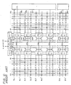
- Fig. 13A is a timing chart showing reading operation of the conventional semiconductor memory
- Fig. 13B is a graph showing power supply peak currents of the conventional sense amplifier drive control circuits where the time base thereof is the same as that of Fig. 13A.
- the conventioanl semiconductor memory generally comprises main amplifiers MA1 and MA2, sense amplifier drive control circuits PLC1 and PLC2, sense amplifiers SAR1, SAR2, ..., and SARn (n: natural number), and SAL1, SAL2, ..., and SALn, bit lines BR1, BR2, ..., and BRn, BR1′, BR2′, ..., and BRn, BL1, BL2, ..., and BLn, and BL1′, BL2′, ..., and BLn′, word lines WR1, WR2, ..., and WRn, and WL1, WL2, ..., and WLn, data lines D1, D1′, D2, and D2′, switching devices SWR1, SWR2, ..., and SWRn, and SWL1, SWL2, ..., and SWLn, switching control lines SWC1, SWC2, ..., and SWCn, memory cells C1, C2, ..., and Cn, and a column
- the bit lines BR1, BR1′, etc. are divided into a plurality of groups each having two bit lines, and each of the groups is respectively connected to the sense amplifiers SAR1, SAR2, etc.
- the memory cell Cn is connected to the word line WRp where p is odd and to the bit line BRn′, and the memory cell Cn′ is connected to the word line WRm where m is even and to the bit line BRn as shown in Fig. 10.
- the switching control line SWCn is connected to the swithing devices SWRn, SWRn′, SWLn, and SWLn′.
- the sense amplifiers SAR1, SAR2, ..., and SARn are connected to the data lines D1 and D1′ via the respective switching devices SWR1 and SWR1′, SWR2 and SWR2′, ..., SWRn and SWRn′, and the same amplifiers SAL1, SAL2, ..., and SALn are connected to the data lines D2 and D2′ via the respective switching devices SWR1 and SWR1′, SWR2 and SWR2′, ..., SWRn and SWRn′.
- the sense amplifier drive control circuits PLC1 and PLC2 are respectively connected to all the sense amplifiers SARn, and all the sense amplifier SALn.
- the switching control line SWC1 connecting with the switching devices SWR1 and SWR1′ is selected by the column decoder CO to transmit the information to the data lines D1 and D1′. After this, the information is sent to an output circuit (not shown) via the main amplifier MA1.
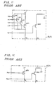
- Fig. 12 shows a general sense amplifier drive control circuit including transistors QP4 and QN1.
- a signal L is inputted into an input terminal PL4, and a signal H is inputted into an input terminal NL1. Therefore, all sense amplifiers which are connected to the sense amplifier drive control circuit become active at the same time. In this sense amplifier drive control circuit, thus, the peak current at the onset of such a sense amplifier operation becomes large.
- Fig. 11 shows a circuit diagram of an improved conventional sense amplifier drive control circuit having transistors QP0, QP1, QP2, QP3, and QN0
- Fig. 13A is a timing chart in the sense amplifier drive control circuit of Fig. 11.
- a signal L is inputted into only an input terminal PL0
- a signal H is inputted into an input terminal NL0 and input terminals PL1, PL2, and PL3.
- a signal L is subsequently inputted into only the input terminal PL1, only the input terminal PL2, and only the input terminal PL3 at an interval.
- the current is applied to the sense amplifiers by stages so that the peak current can be reduced.
- the improved peak current is approximately 1/2 of the same in the general sense amplifier drive control circuit of Fig. 12.
- the semiconductor memory of a first embodiment of the present invention generally comprises a main amplifier MA, sense amplifier drive control circuits PLC1′, PLC2′, ..., and PLCn′ each connected to a power supply line Vcc and a grand line Vss, sense amplifiers SA1, SA2, ..., and SAn (n: natural number), bit lines B1, B2, ..., and Bn, and B1′, B2′, ..., and Bn′, ..., and Bn′, word lines W1, W2, ..., data lines D, D′ connected to the main amplifier MA, switching devices SW1, SW1′, SW2, SW2′, ..., SWn and SWn′, switching control lines SWC1′, SWC2′, ..., and SWCn′, memory cells MC1, MC2, ..., and MCn, and a column decoder CO′.
- main amplifier MA sense amplifier drive control circuits PLC1′, PLC2′, ..., and PLCn′ each connected to a power supply line Vc
- the bit lines B1, B1′, etc. are divided into a plurality of groups each having two bit lines Bn and Bn′, and each of the groups is respectively connected to the sense amplifiers SA1, SA2, ..., SAn.
- the memory cell MCn is connected to the word line Wp where p is odd and to the bit line Bn′, and the memory cell MCn′ is connected to the word line Wm where m is even and to the bit line Bn as shown in Fig. 1.
- the switching control line SWCn′ is connected to the swithing devices SWn, SWn′ for controlling the switching thereof.
- the sense amplifiers SA1, SA2, ..., and SAn are connected to the data lines D and D′ via the respective switching devices SW1 and SW1′, SW2 and SW2′, ..., and SWn and SWn′.
- the sense amplifier drive control circuits PLC1′, PLC2′, ..., and PLCn′ are respectively connected to the sense amplifiers SA1, SA2, ..., and SAn via a pair of sense amplifier power lines SPLn and sense amplifier grand line SNLn.
- the sense amplifier SA1 has a power line SPL1 and a grand line SNL1
- the sense amplifier SA2 has a power line SPL2 and a grand line SNL2.
- FIG. 2 A circuit diagram of the sense amplifier SAn is shown in Fig. 2, and circuit diagrams of the sense amplifier drive control circuit PLCn′ and the column decoder CO′ are shown in Fig. 3A.
- the sense amplifier SA1 includes P-type metal oxide semiconductor transistors (PMOS transistors) MPS1 and MPS2 and N-type metal oxide semiconductor transistors (NMOS transistors) MNS1 and MNS2.
- the sense amplifier drive control circuit PLCn includes a PMOS transistor MPn, an NMOS transistor MNn, and an inverter Vn.
- the PMOS transistors MP1, MP2, ..., and MPn are connected to the power supply line Vcc, and the NMOS transistos MN1, MN2, ..., and MNn are connected to the grand line Vss.
- the column decoder CO′ includes column address control circuits COC1, ..., and COCn each having a column address selecting circuit, and a NAND gate and an inverter.
- the column decoder COC1 includes a column address selecting circuit CD1, a NAND gate 11, and an inverter 12.
- the column address selecting circuits CD1, CD2, ..., and CDn are connected to address lines AD, and the NAND gates 11, ..., 1n are connected to a switching signal line SW.
- An output signal from the column address selecting circuits CD1, CD2, ..., and CDn is respectively inputted into the corresponding NAND gate 11, etc.
- the switching signal on the switching signal line SW becomes high for a predetermined time period in every writing operation.
- Fig. 3B shows a circuit diagram of the column address selecting circuit of Fig. 3A.
- Each of the column address selecting circuits CD1, CD2, ..., and CDn includes a NAND gate NA and an inverter INV.
- the NAND gate NA In the input of the NAND gate NA, only one address is determined by the number of inverter IV.
- one column address output signal CO′ is outputted in accordance with the address signals on the address lines AD.
- Fig. 3B there are twenty-four kinds of column address because the number of address lines n is 4.
- the bit lines B1, B1′, B2, B2′, ..., and Bn′ are determined at the same voltage level at first.
- a word line W1 is selected
- information of the memory cells MC1, MC2, ..., and MCn which are connected to such a selected word line W1 is respectively transmitted to the bit lines B1′, B2′, ..., and Bn′ which are connected to such selected meory cells MC1, MC2, etc. Therefore, the information is sent to the sense amplifiers SA1, SA2, ..., and SAn.
- a column address selecting signal CO′1 is outputted to the sense amplifier drive control circuit PLC1′, and a switching control signal is also produced by the COC1 for outputting to the switching devices SW1 and SW1′ via the switching control line SWC1′.
- the MOS transistors MP1 and MN1 are driven by the column address selecting signal CO′1 so that the sense amplifier driving signals are supplied, via the sense amplifier power supply line SPL1 and the sense amplifier grand line SNL1, to the sense amplifier SA1.
- the MOS transistors MNS1, MNS2, MPS1, and MPS2 are driven by the sense amplifier driving signals whereby the information on the bit lines B1 and B1′ is amplified and sent to the switching devices SW1 and SW1′.
- the switching devices SW1 and SW1′ are made active by the switching control signal via the switching control line SWC1′, the information on the bit line B1 is transmitted to the data line D, and the information on the bit line B1′ is transmitted to the data line D′.
- the transmitted informaiton on the data lines D and D′ is thus applied to the main amplifier MA.
- Fig. 4 is a circuit diagram showing another sense amplifier drive control circuit according to a second embodiment of the present invention.
- the sense amplifier drive control circuit of Fig. 4 has substantially the same structure as that of Fig. 3 except that MOS transistors MPS1′, ..., and MPSn′ are further provided in the sense amplifier drive control circuits PLC1′, ..., and PLCn′, and that a sense amplifier control signal line PLS is also provided so as to be connected to the MOS transistors MPS1′, ..., and MPSn′.
- a control signal in which a word line selecting signal (not shown) selecting word line W1, W2, ..., and Wn is delayed is applied.
- a word line selecting signal not shown
- PMOS transistors MPS1′, ..., and MPSn′ are respectively connected, via the inverters IS1, .., and ISn, to control signal line PLS.
- the power supply line Vcc is connected, via the PMOS transistors MP1 and MPS1′, to the grand line Vss.
- the control signal on the control line signal PLS becomes high when one of the word lines W1, W2, ..., and Wn is selected, so that all MOS transistors MPS1′, MNS1′, MPS2′, MNS2′, ..., and MNSn′ are made active.
- Fig. 5 shows only current curves, voltage curves of Fig. 13A may be used in combination with Fig. 5. Whe using Fig. 13A in combination with Fig. 5, the voltage curve NL0, NL1 also indicates a voltage PLS in Fig. 4. Thus, in the present invention, the peak current is approximately 1/4 of the general conventional semiconductor memory.
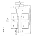
- Fig. 6 shows a block diagram of a semiconductor memory of the invention as an integrated circuit design.
- the data lines D1, D1′, D2, and D2′ and the word lines WR1, WL1, WR2, WL2, ..., and WL2 are provided so as to be made normal to the bit lines B1, B1′, B2, B2′, ..., and Bn′.
- the sense amplifier driving lines SPL1, SNL1, ..., and SNLn are provided so as to be made parallel to the bit lines B1, B1′, B2, B2′, ..., and Bn′.
- bit lines B1, B1′, ..., and Bn′ is formed in a first layer; the word lines WR1, WL1, ..., and WLn and the data lines D1, D1′ D2, and D2′ are formed in a second layer; and the sense amplifier driving lines SPL1, SNL1, ..., and SNLn are formed in a third layer. Therefore, since the sense amplifiers having the same column address can be connected to the same sense amplifier driving lines, an efficient layout can be achieved.
- Fig. 7 is a block diagram of a semiconductor memory suitable for a video memory according to the invention.
- the semiconductor memory of Fig. 7 has substantially the same structure as that of Fig. 6 except that a parellel-to-serial converting circuit 41 is provided so as to be arranged between the main amplifiers MA1 and MA2 and an output circuit (not shown).
- the present semiconductor memory can be applied to a video memory in which column address data is subsequently inputted therein or outputted therefrom.
- Fig. 8 is a block diagram of a semiconductor memory of another design according to the present invention.
- the semiconductor memory comprises four memory blocks MB1, MB2, MB3, and MB4, an input/output port 31, an address input buffer ADB, a row predecoder PR, and a block selecting circuit SE.
- Fig. 9A is a circuit diagram of the block selecting circuit includes four NAND gates S1, S2, S3, and S4 respectively connected to four inverters T1, T2, T3, and T4, and produced block signals BL1, BL2, BL3, and BL4 are respectively sent to the memory blocks MB1, MB2, MB3, and MB4 for making active only one memory block.
- Fig. 9A is a circuit diagram of the block selecting circuit includes four NAND gates S1, S2, S3, and S4 respectively connected to four inverters T1, T2, T3, and T4, and produced block signals BL1, BL2, BL3, and BL4 are respectively sent to the memory blocks MB1, MB2, MB3, and MB4 for making
- FIG. 9B shows a circuit diagram of the row predecoder when the number of address line na is 6.
- the row predecoder PR includes NAND gates GA and invereters E and F each connected to the corresponding NAND gate GA.
- Each of the memory blocks MB1, MB2, MB3, and MB4 has the same structure of the semiconductor design of Fig. 1 except that a row decoder (not shown) is provided between word lines WR1, WL1, ..., and WLn and the row predecoder PR.
- the output signal from the parallel-to-serial converting circuit 41 is sent to a data line DT, and then transmitted to the input/output port 31.
- Address signals of an na-bits is inputted, via the address input buffer ADB, to the row predecoder PR.
- two bit-lines for selecting the memory blocks MB1 to MB4 are connected to the block selecting circuit SE, and produced signals on ma-lines X11, X12, X13, X14, X21, X22, X23, and X24 which are formed of 2(na-2) bit-lines are sent to the memory blocks MB1, MB2, MB3, and MB4 by means of the remaining bit-lines, i.e. (na-2) bit-lines in the inputted address lines of the row predecoder PR.
- sixteen address lines can be respectively connected to the word lines WR1, WL1, ..., and WL8 in total.
- the sense amplifier driving current is so small, the power supply peak current can be considerably reduced in the semiconductor memory structure of the present invention.
- the time for designing such semiconductor memories can be also reduced.
- a semiconductor memory including memory cells each connected to one of a first set of lines for selecting column address signal and to one of a second set of lines for selecting a row address signal, decoder responsive to address signals and a switching signal for producing a column address selecting signal and switching control signal, sense amplifier drive control circuit responsive to the column address selecting signal for producing sense amplifier driving signals, sense amplifier circuit responsive to the sense amplifier driving signals and the column address signal for amplifying the column address signal in response to the sense amplifier driving signals, and switching device responsive to the amplified sense amplifier driving signals and the switching control signal for outputing the amplified sense amplifier driving signals to data lines.
- the sense amplifier driving current can be made so small, the power supply peak current can be considerably reduced.
Landscapes
- Engineering & Computer Science (AREA)
- Microelectronics & Electronic Packaging (AREA)
- Computer Hardware Design (AREA)
- Dram (AREA)
Applications Claiming Priority (2)
| Application Number | Priority Date | Filing Date | Title |
|---|---|---|---|
| JP332011/87 | 1987-12-28 | ||
| JP33201187 | 1987-12-28 |
Publications (2)
| Publication Number | Publication Date |
|---|---|
| EP0322902A2 true EP0322902A2 (fr) | 1989-07-05 |
| EP0322902A3 EP0322902A3 (fr) | 1991-11-06 |
Family
ID=18250143
Family Applications (1)
| Application Number | Title | Priority Date | Filing Date |
|---|---|---|---|
| EP19880121810 Withdrawn EP0322902A3 (fr) | 1987-12-28 | 1988-12-28 | Mémoire à semi-conducteurs fonctionnant avec un courant de pointe bas |
Country Status (2)
| Country | Link |
|---|---|
| EP (1) | EP0322902A3 (fr) |
| KR (1) | KR890010917A (fr) |
Cited By (1)
| Publication number | Priority date | Publication date | Assignee | Title |
|---|---|---|---|---|
| GB2286271A (en) * | 1994-01-31 | 1995-08-09 | Advanced Risc Mach Ltd | Data memory with sense amplifier |
Family Cites Families (6)
| Publication number | Priority date | Publication date | Assignee | Title |
|---|---|---|---|---|
| JPS5484936A (en) * | 1977-12-20 | 1979-07-06 | Fujitsu Ltd | Decoder circuit |
| US4162540A (en) * | 1978-03-20 | 1979-07-24 | Fujitsu Limited | Clocked memory with delay establisher by drive transistor design |
| JPS58147884A (ja) * | 1982-02-26 | 1983-09-02 | Toshiba Corp | ダイナミック型半導体記憶装置 |
| US4542483A (en) * | 1983-12-02 | 1985-09-17 | At&T Bell Laboratories | Dual stage sense amplifier for dynamic random access memory |
| US4758993A (en) * | 1984-11-19 | 1988-07-19 | Fujitsu Limited | Random access memory device formed on a semiconductor substrate having an array of memory cells divided into sub-arrays |
| KR900005667B1 (ko) * | 1984-11-20 | 1990-08-03 | 후지쓰 가부시끼가이샤 | 반도체 기억장치 |
-
1988
- 1988-12-28 EP EP19880121810 patent/EP0322902A3/fr not_active Withdrawn
- 1988-12-28 KR KR1019880017631A patent/KR890010917A/ko not_active Ceased
Cited By (3)
| Publication number | Priority date | Publication date | Assignee | Title |
|---|---|---|---|---|
| GB2286271A (en) * | 1994-01-31 | 1995-08-09 | Advanced Risc Mach Ltd | Data memory with sense amplifier |
| US5602787A (en) * | 1994-01-31 | 1997-02-11 | Advanced Risc Machines Limited | Data memory with sense amplifier and method of operation |
| GB2286271B (en) * | 1994-01-31 | 1998-02-18 | Advanced Risc Mach Ltd | Data memory with sense amplifier |
Also Published As
| Publication number | Publication date |
|---|---|
| KR890010917A (ko) | 1989-08-11 |
| EP0322902A3 (fr) | 1991-11-06 |
Similar Documents
| Publication | Publication Date | Title |
|---|---|---|
| KR100241079B1 (ko) | 병렬 데이터 초기화기능을 가진 멀티포트 메모리셀및 메모리 | |
| KR100314491B1 (ko) | 반도체 기억 장치 | |
| JPH04228188A (ja) | 半導体記憶装置 | |
| US4951259A (en) | Semiconductor memory device with first and second word line drivers | |
| US7408801B2 (en) | Nonvolatile semiconductor memory device | |
| EP0319691B1 (fr) | Dispositif de mémoire à semi-conducteurs | |
| US4247921A (en) | Decoder | |
| KR950001289B1 (ko) | 반도체기억장치 | |
| US5227697A (en) | Dynamic type semiconductor memory | |
| US8693264B2 (en) | Memory device having sensing circuitry with automatic latching of sense amplifier output node | |
| US5777925A (en) | Semiconductor non-volatile memory device | |
| CN1121693C (zh) | 半导体存储装置及其测试方法 | |
| CA1160742A (fr) | Cellule de memoire a acces selectif statique | |
| CN101064185B (zh) | 存储器 | |
| JPH04285794A (ja) | 半導体記憶装置 | |
| US5245579A (en) | Semiconductor memory device | |
| US6973002B2 (en) | Semiconductor integrated circuit comprising sense amplifier activating circuit for activating sense amplifier circuit | |
| US5742540A (en) | Semiconductor memory and layout/circuit information generating apparatus | |
| EP0322902A2 (fr) | Mémoire à semi-conducteurs fonctionnant avec un courant de pointe bas | |
| US5838606A (en) | Three-transistor static storage cell | |
| US6072713A (en) | Data storage circuit using shared bit line and method therefor | |
| KR19990041459A (ko) | 반도체 메모리장치의 셀 어레이 제어장치 | |
| EP0488672B1 (fr) | Dispositif de mémoire avec des amplificateurs de détection de type courant à miroir | |
| US5828618A (en) | Line memory | |
| US4661926A (en) | Bit line gain circuit for read only memory |
Legal Events
| Date | Code | Title | Description |
|---|---|---|---|
| PUAI | Public reference made under article 153(3) epc to a published international application that has entered the european phase |
Free format text: ORIGINAL CODE: 0009012 |
|
| 17P | Request for examination filed |
Effective date: 19881228 |
|
| AK | Designated contracting states |
Kind code of ref document: A2 Designated state(s): DE FR GB |
|
| PUAL | Search report despatched |
Free format text: ORIGINAL CODE: 0009013 |
|
| AK | Designated contracting states |
Kind code of ref document: A3 Designated state(s): DE FR GB |
|
| RHK1 | Main classification (correction) |
Ipc: G11C 7/06 |
|
| 17Q | First examination report despatched |
Effective date: 19930126 |
|
| STAA | Information on the status of an ep patent application or granted ep patent |
Free format text: STATUS: THE APPLICATION IS DEEMED TO BE WITHDRAWN |
|
| 18D | Application deemed to be withdrawn |
Effective date: 19930608 |