EP0318055B1 - Datenprozessor mit A/D-Umsetzer, um mehrere analoge Eingabekanäle in Digitaldaten umzusetzen - Google Patents
Datenprozessor mit A/D-Umsetzer, um mehrere analoge Eingabekanäle in Digitaldaten umzusetzen Download PDFInfo
- Publication number
- EP0318055B1 EP0318055B1 EP88119823A EP88119823A EP0318055B1 EP 0318055 B1 EP0318055 B1 EP 0318055B1 EP 88119823 A EP88119823 A EP 88119823A EP 88119823 A EP88119823 A EP 88119823A EP 0318055 B1 EP0318055 B1 EP 0318055B1
- Authority
- EP
- European Patent Office
- Prior art keywords
- data
- analog
- program
- macro service
- service operation
- Prior art date
- Legal status (The legal status is an assumption and is not a legal conclusion. Google has not performed a legal analysis and makes no representation as to the accuracy of the status listed.)
- Expired - Lifetime
Links
Images


Classifications
-
- G—PHYSICS
- G06—COMPUTING; CALCULATING OR COUNTING
- G06F—ELECTRIC DIGITAL DATA PROCESSING
- G06F3/00—Input arrangements for transferring data to be processed into a form capable of being handled by the computer; Output arrangements for transferring data from processing unit to output unit, e.g. interface arrangements
- G06F3/05—Digital input using the sampling of an analogue quantity at regular intervals of time, input from a/d converter or output to d/a converter
Definitions
- the present invention relates to a data processor and, more particularly, to a microcomputer including an analog-to-digital converter (called hereinafter an "A/D converter") for converting a plurality of analog input channels into the corresponding digital data.
- A/D converter an analog-to-digital converter
- a microcomputer including an A/D converter can perform a data processing operation on an analog signal supplied thereto and is thus widely employed in various systems.
- a CPU Central Processing Unit
- the microcomputer supplies a converting command to the A/D converter and then receives the converted digital data to perform the requested processing operation thereon.
- the CPU suspends the operations in a main program routine and saves the contents of a program counter and a status register into a stack area of a data memory, followed by starting an operation in an interruption program routine.
- the program counter is used for reading each instruction out of a program memory and the status register stores status data representative of an executing condition of the CPU.
- the CPU reads the converted data from the A/D converter and transfers it to a predetermined destination area of the data memory.
- the CPU returns the saved contents to the program counter and the status register, respectively, and then resumes the operation in the main program routine.
- the second control method can enhance the execution efficiency of the CPU.
- the CPU suspends the program operation which is currently being executed, inhibits the contents of the program counter and status register from being varied, and then transfers the converted data to the destination area without saving the contents of the program counter and status register and with holding them as they are. After the converted data is transferred to the destination area, the CPU allows the program counter and status register to change to resume the suspended program operation.
- the second type of interruption operation is also called "macro service operation". According to the macro service operation, the above-mentioned overheads are not required, so that the execution efficiency and processing capability of the CPU are enhanced remarkably.
- an object of the present invention is to provide a microcomputer performing a macro service operation for a plurality of analog input channels.
- Another object of the present invention is to provide a data processor which can transfer the converted data of plural analog input channels to respective destination areas in a data memory without intervention of any user's program operation.
- Still another object of the present invention is to provide an improved data processor including an A/D converter for a plurality of analog inputs.
- a data processor according to the present invention is characterized in claim 1.
- the A/D conversion for a plurality of analog inputs can be designated and reserved simultaneously, and the execution of the A/D conversion of the respectived designated analog inputs and the transfer of the respective converted data can be performed in a sequential manner by the macro service operation without intervention of any user's program and without any overhead.
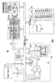
- a microcomputer 1000 includes a CPU (Central Processing Unit) 100.
- a program to be executed by the CPU 100 is stored in a program memory 200.
- This program includes a main operation routine and one or more interruption operation routines and is made up by a user of the microcomputer 100.
- the CPU 100 includes a program counter (PC) 101 indicating an address of an instruction to be executed in the program of the program memory 200, an instruction register (IR) 105 stored with an instruction read from the program memory 200, an instruction decoder (ID) 106 decoding the instruction from the IR 105 and producing various control signals, an execution control unit 107 responding to the control signals from the ID 106 to control the whole operation of the microcomputer 1000, an arithmetic and logic unit (ALU) 103 performing an arithmetic and/or logic operation, a status register (PSW) 104 storing information representative of an execution condition of the CPU 100, and a general purpose register set 102, which are interconnected via an address/data bus 600.
- PC program counter
- IR instruction register
- ID instruction decoder
- ALU arithmetic and logic unit
- PSW status register
- 104 storing information representative of an execution condition of the CPU 100
- a general purpose register set 102 which are interconnected via an address/data bus 600.
- the execution control unit 107 includes a micro-ROM (Read Only Memory) 1071 and a pointer 1072 pointing out an address of the micro-ROM 1071.
- the micro-ROM 1071 stores a microprogram consisting of a string of microinstructions for a macro service operation which will be described later in detail.
- a data memory 300, an A/D converter 400 and a converted-data operation controller 500 are also interconnected.
- the A/D converter 400 includes a start flag 401, a converted result register (CRR) 402 and a selection data register (ASR) 403 and starts to execute the A/D conversion when the start flag 401 is set.
- the A/D converter 400 is supplied with eight channels of analog inputs 400-1 to 400-8, one of which is selected in response to the selection data stored in the ASR 403.
- the converted digital data of the selected analog input is stored into the CRR 402.
- the A/D converter 400 When the A/D conversion is completed, the A/D converter 400 generates a completion signal 400-9 which is in turn to the converted-data operation controller 500.
- one of the analog inputs 400-1 to 400-8 is selected in response to the selection data of the ASR 403 as shown in the following TABLE:
- the A/D converter 400 of this type further includes a selector 404, a sample/hold circuit 405, a comparator 406, a comparison voltage generater 407, a sequential comparison register 408 and a controller 410, as well know in the art.
- the controller 410 starts the A/D converting operation when the start flag 401 is set, and generates the completion signal 400-9 when the converted digital data is stored into the CRR 402.
- the further detailed description on the A/D converter of that type will be omitted since the circuit operation thereof is well-known in the art.
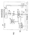
- This unit 501 includes a mode flag 502 for designating either one of a macro service operation and an interruption operation on the converted digital data and a channel pointer address register (ACPTR) 503 storing an address of a channel pointer (CPTR) 302 which will be described later.
- ACPTR channel pointer address register
- the operation request unit 501 supplies an operation request signal 500-1 and an operation mode designation signal 500-2 to a request receiving unit 504.
- the made flag 502 is set to store the data of "1" and the mode designation signal 500-2 takes a high level (logic-1).
- the mode flag 502 is reset to store the data of "0" and the signal 500-2 takes a low level (logic-0). Since the mode flag 502 can be made access, the user can designate the operation mode to the macro service operation or the interruption operation.
- the request receiving unit 504 responds to the request signal 500-1 and detects the level of the mode designation signal 500-2. When the signal 500-2 is of the high level, the unit 504 transfers a macro service code stored in a register 505 to the instruction register (IR) 105 via an operation request bus 507. On the other hand, when the signal 500-2 is of the low level, an interruption code stored in a register 506 is transferred to the IR 105 via the bus 507.
- the interruption code includes a vector address for an interruption program routine stored in the program memory 200.
- the registers 503, 505 and 506 are inhibited from being accessed by the user.
- the data memory 300 includes a stack area 301 into which the contents of PC 101, PSW 104 and register set 102 are saved in response to the interruption operation request, eight destination areas (DST1 to DST8) 304 to 311 to which the converted digital data of the analog inputs 400-1 to 400-8 are respectively transferred, a converted channel register (ACR) 303 storing channel designation data for designating one or more analog inputs to be converted, and a channel pointer (CPTR) 302 storing an address of the ACR 303.
- the ACR 303 has an 8-bits construction, and the respective bits thereof correspond to the respective ones of the analog inputs 400-1 to 400-8.
- the address of the ACR 303 can be selected by the user, but the ACR 303 and the destination areas 304 to 311 are allotted to consecutive addresses, respectively.
- the address of the CPTR 302 is fixed.
- Instructions for the program stored in the memory 200 are read out and executed sequentially by the CPU 100 using the PC 101.
- the ACR 302 is stored with the channel designation data in which bit or bits corresponding to the analog input or inputs to be converted are set to "1" and the CPTR 302 is stored with the address of the ACR 302.
- the mode flag 502 is set to "1" by an instruction from the memory 200.
- the conversion start instruction is read from the memory 200 and executed by the CPU 100, the selection data responsive to the channel designation data of the ACR 303 is stored into the ASR 403 and the start flag 401 is set.
- the conversion priority order of the first to eight analog inputs 400-1 to 400-8 is designed to be in that order. Assuming that the ACR 303 stores the channel designation data of "10001010", therefore, the selection data of "000" for selecting the first analog input 400-1 is set into the ASR 403.
- the A/D converter 400 selects the first analog input 400-1 and starts the A/D converting operation.
- the access to the program memory 200 is allowed during the converting operation by the A/D converter 400. Accordingly, the CPU 100 continues to perform the subsequent operations is parallel to the operation of the A/D converter 400.
- the A/D converter 400 When the conversion of the first analog input 400-1 is completed, the A/D converter 400 generates and applies the completion signal 400-9 to the operation request unit 501.
- the converted digital data is stored in the CRR 402.
- the unit 501 thereby produces the request signal 500-1 with the mode designation signal 500-2 being the high level, since the mode flag 502 is in the set condition.
- the request receiving unit 504 transfers and sets the macro service code of the register 505 to the IR 105 via the bus 507.
- the macro service code is decoded by the ID 106 and supplied to the execution control unit 107.
- the execution control unit 107 produces and applies a hold signal 107-1 to the PC 101, PSW 104 and the register set 107 to inhibit the contents thereof from being varied and to hold the current contents thereof as they are.
- the pointer 1072 is set with a leading address of the microprogram for the macro service operation stored in the micro-ROM 1071, so that the macro service operation starts to be executed.
- the CPU 100 suspends the program operation and then performs the macro service operation without saving the contents of the PC 101, PSW 104 and register set 102 and with holding the current contents thereof as they are.
- the macro service operation is performed in accordance with the flow chart shown in Fig. 3. Since the ACPTR 503 of the operation request unit 501 stores the address of the CPTR 302, the execution control unit 107 makes access to the CPTR 302 to read the content thereof by use of the address stored in the ACPTR 503 (Step 30).
- the content of the CPTR 302 indicates the address of the ACR 303, and the destination areas 304 to 311 are allotted respectively to the consecutive addresses from the address next the address of the ACR 303. That is, the address of the destination area to be transferred with the converted digital data is equal to the address obtained by adding the content of the ASR 403 plus 1 to the address of the ACR 303.
- the execution unit 107 adds the content of the ASR 403 plus 1 to the content of the CPTR 302 by using the ALU 103 (Step 31). Since the content of the ASR 403 is "000", the added result is equal to the address of the first destination area (DST1) 403.
- the execution control unit 107 makes access to the area 403 by use of the added result to transfer the converted digital data of the first analog input 400-1 to the first destination area 304 from the CRR 402 (Step 32). Thereafter, the execution control unit 107 makes access again to the CPTR 302 by use of the content of the ACPTR 503 (Step 33) and then makes access to the ACR 303 by use of the content of the CPTR 302 (Step 34).
- the execution control unit 107 Since the converted digital data has been already transferred to the associated destination register, the execution control unit 107 resets the bit of the channel designation data of the ACR 303, which bit position corresponds to the content of the ASR 403 (Step 35). The channel designation data is thereby changed "00001010". The execution control unit 107 thereafter scans the content of the ACR 303 from the least significant bit (LSB) thereof by using the ALU 103 (Step 36) and detects whether or not another bit set to "1" is present in the channel designation data (Step 37). Since the fifth bit is set to "1", the position data thereof, "100", is set into the ASR 403 as new selection data by the unit 107 (Step 38).
- LSB least significant bit
- the A/D converter is thereby initialized and then selects the fifth analog input 400-5 to start the A/D conversion.
- an access-enable command to the program memory 200 is produced (Step 40), so that the hold signal 107-1 is withdrawn.
- the PC 101, PSW 104 and register set 102 are thereby allowed to change the contents thereof so the CPU 100 restarts to read and execute the instructions from the program memory 200.
- the macro service operation responsive to the completion signal 400-9 is completed and the CPU resumes the suspended program operation.
- the signal 400-9 is generated again.
- the CPU 100 suspends the program operation with holding the contents of the PC 101, PSW 104 and register set 102 as they are and then performs the macro service operation.
- the converted digital data of the fifth analog input 400-5 is thereby transferred to the fifth destination area (DST 5) 308.
- the A/D conversion of the seventh analog input 400-7 is then started, and the CPU 100 restarts to execute the suspended program operation.
- the channel designation data of the ACR 303 is changed to all "0" by the execution of Step 35, so that it is detected that the content of the ACR 303 is all "0" in Step 37. Accordingly, the execution control unit 107 resets the start flag 401 of the A/D converter 400 to bring the converter 400 into a standby condition.
- the operation request unit 501 produces the request signal 500-1 with the low level mode designation signal 500-2. Accordingly, the request receiving unit 504 sets the interruption code 506 to the IR 105.
- the execution control unit 107 saves the contents of the PC 101, PSW 104 and register set 102 into the stack area 301 of the data memory 300 and thereafter sets into the PC 101 the vector address for the interruption program routine. The CPU 100 thereby executes the interruption operation in accordance with the interruption program routine. When the interruption operation is completed, the saved contents are returned respectively to the PC 101, PSW 104 and register set 102 from the stack area 301, and the suspended main program routine is restarted.
- a microcomputer 1000′ according to another embodiment of the present invention, wherein the same constituents as those shown in Fig. 1 are denoted by the same reference numerals to omit further description thereof.
- a memory pointer (MPTR) 320 is provided at an address next the address of the ACR 300, and the address of the first destination area (DST1) 304 is stored in the MPTR 320. Therefore, the address of the destination areas 304 to 311 can be designed independently of the address of the ACR 303.
- the macro service operation in this microcomputer 1000′ is basically the same as that shown in Fig. 3, but due to the presence of the MPTR 320, Steps 31-1, 31-2 and 31-3 are executed in place of Step 31 of Fig.
- Step 31-1 the content of the CPTR 302 is incremented by one by using the ALU 103. Since the incremented result is equal to the address of the MPTR 320, the MPTR 320 is made access by use of the incremented result (Step 31-2), and the content of the MPTR 320 is added with the content of the ASR 403 by using the ALU 103 (Step 31-3). The added result is equal to the address of the destination area to be transferred with the converted digital data.
- the Steps 32 to 40 are thereafter executed in the same manner as shown in Fig. 3.
- the MPTR 320 can take two or more bytes, so that the destination areas 304 to 311 can be allotted to arbitrary addresses of the data memory 300.
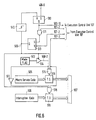
- FIG. 6 there is shown a circuit construction representative of one example of the converted-data operation controller 500 shown in Figs. 1 and 4, wherein the ACPTR 503 is omitted in order to avoid the complication of the drawing.
- a flip-flop called hereinafter an "F/F" 510 is set and the Q-output thereof is supplied to the execution control unit 107 as an operation request control signal 500-10.
- the execution control unit 107 produces an acknowledge signal 107-2 after a current instruction is completed to be executed, so that an F/F 513 is set through an AND gate 511.
- the Q-output of the F/F 513 is used as the operation request signal 500-1.
- the leading edge of this signal is detected by a detector 510 to reset the F/F 510.
- the F/F 510 thereby waits for the next conversion completion signal 400-9.
- the signal 500-1 activates a tri-state buffer 514, so that the content of the mode flag 502 is read out therefrom.
- the signal 500-1 is further supplied to AND gates 515 and 518.
- the AND gate 515 further receives the content of the mode flag 502, whereas the AND gate 518 receives the inverted content of the mode flag 502 by an inverter 517. Therefore, the AND gate 515 is opened by the set state of the mode flag 502, whereas the AND gate 518 is opened by the reset state of the mode flag 502.
- one of transfer gates 516 and 519 is thereby brought into an open state, so that the macro service operation code 505 or the interruption operation code 506 is outputted to the but 507.
- the execution control unit 107 produces an operation and signal 107-2 to reset the F/F 513.
- the buffer 514 and transfer gates 516 and 519 are thereby brought into a closed state.
- the data processor or microcomputer according to the present invention can be perform any one of the software interruption operation and the macro service operation is response to the A/D conversion completion signal, and moreover the macro service operation for a plurality of analog inputs is performed.
- the present invention is not limited the above embodiments, but may be changed and modified without departing from the scope and spirit of the invention.
- the A/D converter 400 can be constructed to generate the conversion completion signal 400-9 with resetting the start flag 401 and in that case, a step for setting the start flag is inserted after Step 38 shown in Fig. 3 and Step 39 can be omitted.
- the program memory 200 and the data memory 300 can be constructed by a single memory.
- the request receiving unit 504 may transfer the macro service code or the interruption code to the IR 105 via the address/data bus 600 in place of the bus 507.
Claims (4)
- Datenprozessor mit einem Programmspeicher (200), der ein Programm speichert, einer zentralen Prozessoreinheit (100), die einen Programmzähler (101) enthält, der die Adresse des Programmspeichers enthält, der eine auszuführende Instruktion speichert und einem Statusregister (104), das temporär Information speichert, die repräsentativ ist für den Exekutionsstatus der zentralen Prozessoreinheit und das das Programm durchführt durch Benutzung des Programmzählers und des Statusregisters, einem Analog-Digital-Konverter (400) der mit einer Vielzahl von analogen Eingangssignalen (400-1 bis 400-8) versorgt wird und eine erste Speichervorrichtung (403) enthält, die temporär Daten speichert zum Auswählen eines der analogen Eingangssignale, wobei der Analog-Digital-Konverter eines der analogen Eingangssignale auswählt in Antwort auf die Daten, die in der ersten Speichervorrichtung gespeichert sind, die ausgewählten analogen Eingangssignale konvertiert in digitale Daten und ein Vollendungssignal (400-9) erzeugt, das die Vollendung der Analog-Digital-Konversion bedeutet, und einer Vorrichtung (500), die in Antwort auf das Vollendungssignal eine Makroservice-Operations-Anfrage (507) zur zentralen Prozessoreinheit zuführt, wobei die zentrale Prozessoreinheit ferner aufweist eine Ausführungsvorrichtung, die in Antwort auf die Makroservice-Operations-Anfrage die Durchführung des Programmes unterbricht und die Makroservice-Operation durchführt, wobei die Makroservice-Operation durchgeführt wird ohne Speicherung der Inhalte des Programmzählers und des Statusregisters und mit Beibehaltung deren Inhalte wie sie sind, wobei die Ausführungsvorrichtung zum Ausführen der Makroservice-Operation eine Vorrichtung (30-32) enthält zum Übertragen der digitalen Daten zu einem vorbestimmten Zielfeld (304-311) und eine Vorrichtung (40) zum Neustarten der Inhaltsänderung des Programmzählers und des Statusregisters, um der zentralen Prozessoreinheit zu ermöglichen, die unterbrochene Operation des Programms wiederaufzunehmen, nachdem das digitale Datum zum vorbestimmten Zielfeld übertragen wurde,
dadurch gekennzeichnet, daß der Datenprozessor ferner aufweist eine zweite Speichervorrichtung (303) zum temporären Speichern von Zieldaten zum Bestimmen eines oder mehrere Analog-Eingangssignale für die Konversion und daß die Exekutionsvorrichtung zum Durchführen der Makroservice-Operation ferner eine Vorrichtung 33 bis 37 enthält zum Detektieren des Zieldatums, das in der zweiten Speichervorrichtung gespeichert ist, um entsprechend neue Selektionsdaten zu produzieren, zum Auswählen eines analogen Eingangssignals, das als nächstes konvertiert werden soll, und eine Vorrichtung (38) zum Setzen des neuen Selektionsdatums in der ersten Speichervorrichtung, so daß der Analog-Digital-Konverter den Konversionsbetrieb startet auf das analoge Eingangssignal, das durch das neue Selektionsdatum ausgewählt wurde. - Datenprozessor nach Anspruch 1,
dadurch gekennzeichnet, daß die Zieldaten, die in der zweiten Speichervorrichtung (403) gespeichert sind, aus einer Vielzahl von Bits besteht, die jeweils den entsprechenden des analogen Eingangssignals entsprechen, und daß die Detektorvorrichtung eine Vorrichtung (35) enthält zum Rücksetzen des Bits des Zieldatums, welches dem konvertierten, analogen Eingangssignal entspricht, und eine Vorrichtung (36, 37) zum Beurteilen, ob ein weiteres Bit, das den gesetzten Zustand annimmt, im Zieldatum vorliegt, oder nicht. - Datenprozessor nach Anspruch 2,
dadurch gekennzeichnet, daß die Durchführungsvorrichtung (39) zum Durchführen der Makroservice-Operation ferner eine Vorrichtung enthält zum Überführen des Analog-Digital-Konverters in einen Wartezustand, wenn alle Bits des Zieldatums in rückgesetztem Zustand sind. - Datenprozessor nach Anspruch 1, 2 oder 3,
dadurch gekennzeichnet, daß das vorbestimmte Zielfeld eine Vielzahl von Speicherfeldern (304 - 311) enthält, die jeweils vorgesehen sind, um die digitalen Daten des zugehörigen der analogen Eingangssignale zu speichern.
Applications Claiming Priority (2)
| Application Number | Priority Date | Filing Date | Title |
|---|---|---|---|
| JP30061487 | 1987-11-27 | ||
| JP300614/87 | 1987-11-27 |
Publications (3)
| Publication Number | Publication Date |
|---|---|
| EP0318055A2 EP0318055A2 (de) | 1989-05-31 |
| EP0318055A3 EP0318055A3 (de) | 1991-10-30 |
| EP0318055B1 true EP0318055B1 (de) | 1995-02-01 |
Family
ID=17886975
Family Applications (1)
| Application Number | Title | Priority Date | Filing Date |
|---|---|---|---|
| EP88119823A Expired - Lifetime EP0318055B1 (de) | 1987-11-27 | 1988-11-28 | Datenprozessor mit A/D-Umsetzer, um mehrere analoge Eingabekanäle in Digitaldaten umzusetzen |
Country Status (3)
| Country | Link |
|---|---|
| US (1) | US4996639A (de) |
| EP (1) | EP0318055B1 (de) |
| DE (1) | DE3852928T2 (de) |
Cited By (1)
| Publication number | Priority date | Publication date | Assignee | Title |
|---|---|---|---|---|
| US6839014B2 (en) | 2001-06-27 | 2005-01-04 | Renesas Technology Corp. | One-chip microcomputer with analog-to-digital converter |
Families Citing this family (28)
| Publication number | Priority date | Publication date | Assignee | Title |
|---|---|---|---|---|
| JPH0212432A (ja) * | 1988-06-30 | 1990-01-17 | Nec Corp | データ処理装置 |
| DE68905028T2 (de) * | 1988-11-17 | 1993-11-11 | Nec Corp | Datenverarbeitungseinrichtung zur Erzeugung einer Folge von Impulsen die eine variable Länge an den Ausgängen aufweisen. |
| DE4015853C2 (de) * | 1990-05-17 | 1999-04-01 | Ako Werke Gmbh & Co | Eingangsschaltung eines Mikrorechners |
| JP3288694B2 (ja) * | 1990-06-11 | 2002-06-04 | 沖電気工業株式会社 | マイクロコンピュータ |
| JP3323009B2 (ja) * | 1994-09-29 | 2002-09-09 | 日本電気株式会社 | データ処理装置 |
| US5613163A (en) * | 1994-11-18 | 1997-03-18 | International Business Machines Corporation | Method and system for predefined suspension and resumption control over I/O programs |
| WO1997011428A1 (en) * | 1995-09-19 | 1997-03-27 | Microchip Technology Incorporated | Microcontroller wake-up function having digitally programmable threshold |
| US6594691B1 (en) * | 1999-10-28 | 2003-07-15 | Surfnet Media Group, Inc. | Method and system for adding function to a web page |
| US7324496B1 (en) | 2002-05-01 | 2008-01-29 | Nxp B.V. | Highly integrated radio-frequency apparatus and associated methods |
| US8478921B2 (en) * | 2004-03-31 | 2013-07-02 | Silicon Laboratories, Inc. | Communication apparatus implementing time domain isolation with restricted bus access |
| US8884791B2 (en) * | 2004-06-29 | 2014-11-11 | St-Ericsson Sa | Keypad scanning with radio event isolation |
| US7248848B2 (en) * | 2004-06-30 | 2007-07-24 | Matthews Phillip M | Communication apparatus including dual timer units |
| US20050008095A1 (en) * | 2004-07-23 | 2005-01-13 | Rush Frederick A. | Apparatus using interrupts for controlling a processor for radio isolation and associated methods |
| US7433393B2 (en) | 2004-07-23 | 2008-10-07 | Nxp B.V. | Apparatus for controlling a digital signal processor for radio isolation and associated methods |
| US8472990B2 (en) * | 2004-07-23 | 2013-06-25 | St Ericsson Sa | Apparatus using interrupts for controlling a processor for radio isolation and associated method |
| US7761056B2 (en) * | 2004-07-23 | 2010-07-20 | St-Ericsson Sa | Method of controlling a processor for radio isolation using a timer |
| US7593482B2 (en) * | 2004-09-30 | 2009-09-22 | St-Ericsson Sa | Wireless communication system with hardware-based frequency burst detection |
| US7567637B2 (en) | 2004-09-30 | 2009-07-28 | St-Ericsson Sa | Wireless communication system and method with frequency burst acquisition feature using autocorrelation and narrowband interference detection |
| US8019382B2 (en) * | 2004-12-29 | 2011-09-13 | St-Ericsson Sa | Communication apparatus having a standard serial communication interface compatible with radio isolation |
| US7778674B2 (en) * | 2004-12-29 | 2010-08-17 | St-Ericsson Sa | Communication apparatus having a SIM interface compatible with radio isolation |
| US7209061B2 (en) * | 2005-03-30 | 2007-04-24 | Silicon Laboratories, Inc. | Method and system for sampling a signal |
| US7805170B2 (en) * | 2005-03-30 | 2010-09-28 | St-Ericsson Sa | System and method for efficient power supply regulation compatible with radio frequency operation |
| US7801207B2 (en) * | 2005-06-24 | 2010-09-21 | St-Ericsson Sa | Signal processing task scheduling in a communication apparatus |
| US7283503B1 (en) | 2005-06-24 | 2007-10-16 | Silicon Laboratories, Inc. | Communication apparatus including a buffer circuit having first and second portions for alternately storing results |
| US7414560B2 (en) * | 2005-06-29 | 2008-08-19 | Shaojie Chen | Wireless communication system including an audio underflow protection mechanism operative with time domain isolation |
| FR2895200B1 (fr) * | 2005-12-20 | 2008-02-22 | Silicon Lab Inc | Procede d'acquisition d'un burst de correction de frequence par un dispositif de radiocommunication, et dispositif de radiocommunication correspondant. |
| EP2375355A1 (de) * | 2010-04-09 | 2011-10-12 | ST-Ericsson SA | Verfahren und Vorrichtung zum Schützen von Speicherinhalt |
| CN105393179B (zh) * | 2014-04-25 | 2017-07-14 | 三菱电机株式会社 | 功能单元、模拟输入单元、可编程控制器系统 |
Family Cites Families (10)
| Publication number | Priority date | Publication date | Assignee | Title |
|---|---|---|---|---|
| US3789365A (en) * | 1971-06-03 | 1974-01-29 | Bunker Ramo | Processor interrupt system |
| US3883852A (en) * | 1973-04-20 | 1975-05-13 | Corning Glass Works | Image scanning converter for automated slide analyzer |
| US4075691A (en) * | 1975-11-06 | 1978-02-21 | Bunker Ramo Corporation | Communication control unit |
| US4085449A (en) * | 1976-11-26 | 1978-04-18 | Paradyne Corporation | Digital modem |
| US4315314A (en) * | 1977-12-30 | 1982-02-09 | Rca Corporation | Priority vectored interrupt having means to supply branch address directly |
| US4246637A (en) * | 1978-06-26 | 1981-01-20 | International Business Machines Corporation | Data processor input/output controller |
| US4404627A (en) * | 1979-05-11 | 1983-09-13 | Rca Corporation | Interrupt signal generating means for data processor |
| US4348720A (en) * | 1979-08-31 | 1982-09-07 | Bell Telephone Laboratories, Incorporated | Microcomputer arranged for direct memory access |
| EP0153764B1 (de) * | 1984-03-02 | 1993-11-03 | Nec Corporation | Informationsverarbeitungseinheit mit Unterbrechungsfunktion |
| GB8510425D0 (en) * | 1985-04-24 | 1985-06-26 | Data Pag Ltd | Data logging unit |
-
1988
- 1988-11-28 DE DE3852928T patent/DE3852928T2/de not_active Expired - Fee Related
- 1988-11-28 EP EP88119823A patent/EP0318055B1/de not_active Expired - Lifetime
- 1988-11-28 US US07/276,970 patent/US4996639A/en not_active Expired - Lifetime
Cited By (1)
| Publication number | Priority date | Publication date | Assignee | Title |
|---|---|---|---|---|
| US6839014B2 (en) | 2001-06-27 | 2005-01-04 | Renesas Technology Corp. | One-chip microcomputer with analog-to-digital converter |
Also Published As
| Publication number | Publication date |
|---|---|
| EP0318055A3 (de) | 1991-10-30 |
| EP0318055A2 (de) | 1989-05-31 |
| DE3852928T2 (de) | 1995-10-05 |
| DE3852928D1 (de) | 1995-03-16 |
| US4996639A (en) | 1991-02-26 |
Similar Documents
| Publication | Publication Date | Title |
|---|---|---|
| EP0318055B1 (de) | Datenprozessor mit A/D-Umsetzer, um mehrere analoge Eingabekanäle in Digitaldaten umzusetzen | |
| EP0464615B1 (de) | Mikrorechner ausgestattet mit einer DMA-Steuerung | |
| US4430706A (en) | Branch prediction apparatus and method for a data processing system | |
| EP0266800B1 (de) | Datenprozessor mit verschiedenen Unterbrechungsverarbeitungsarten | |
| US4349873A (en) | Microprocessor interrupt processing | |
| US4298927A (en) | Computer instruction prefetch circuit | |
| US4542456A (en) | Method and apparatus for performing range checks | |
| US5060148A (en) | Control system for vector processor with serialization instruction for memory accesses for pipeline operation | |
| US5713044A (en) | System for creating new group of chain descriptors by updating link value of last descriptor of group and rereading link value of the updating descriptor | |
| JPH01120660A (ja) | マイクロコンピュータ装置 | |
| EP0240606B1 (de) | Verarbeitungssystem in Pipelinestruktur und Mikroprozessor mit einem derartigen System | |
| US4797816A (en) | Virtual memory supported processor having restoration circuit for register recovering | |
| JP2900627B2 (ja) | 割り込み制御装置 | |
| US4816992A (en) | Method of operating a data processing system in response to an interrupt | |
| JP2526644B2 (ja) | デ―タ処理装置 | |
| US5327565A (en) | Data processing apparatus | |
| JPH0319974B2 (de) | ||
| US5687380A (en) | Macro service processing of interrupt requests in a processing system where a single interrupt is generated for a plurality of completed transactions | |
| US5280604A (en) | Multiprocessor system sharing expandable virtual memory and common operating system | |
| JPH0623947B2 (ja) | 情報処理装置 | |
| JP2847863B2 (ja) | マイクロプロセッサ割込み制御方式 | |
| JPS59144955A (ja) | 情報処理装置 | |
| US5123093A (en) | Operational processor for performing a memory access and an operational process in parallel | |
| JP2847729B2 (ja) | 情報処理装置 | |
| JPS5860347A (ja) | 通信制御装置 |
Legal Events
| Date | Code | Title | Description |
|---|---|---|---|
| PUAI | Public reference made under article 153(3) epc to a published international application that has entered the european phase |
Free format text: ORIGINAL CODE: 0009012 |
|
| 17P | Request for examination filed |
Effective date: 19881128 |
|
| AK | Designated contracting states |
Kind code of ref document: A2 Designated state(s): DE FR GB |
|
| PUAL | Search report despatched |
Free format text: ORIGINAL CODE: 0009013 |
|
| AK | Designated contracting states |
Kind code of ref document: A3 Designated state(s): DE FR GB |
|
| 17Q | First examination report despatched |
Effective date: 19930513 |
|
| GRAA | (expected) grant |
Free format text: ORIGINAL CODE: 0009210 |
|
| AK | Designated contracting states |
Kind code of ref document: B1 Designated state(s): DE FR GB |
|
| REF | Corresponds to: |
Ref document number: 3852928 Country of ref document: DE Date of ref document: 19950316 |
|
| ET | Fr: translation filed | ||
| PLBE | No opposition filed within time limit |
Free format text: ORIGINAL CODE: 0009261 |
|
| STAA | Information on the status of an ep patent application or granted ep patent |
Free format text: STATUS: NO OPPOSITION FILED WITHIN TIME LIMIT |
|
| 26N | No opposition filed | ||
| REG | Reference to a national code |
Ref country code: GB Ref legal event code: IF02 |
|
| REG | Reference to a national code |
Ref country code: GB Ref legal event code: 732E |
|
| REG | Reference to a national code |
Ref country code: FR Ref legal event code: TP |
|
| PGFP | Annual fee paid to national office [announced via postgrant information from national office to epo] |
Ref country code: FR Payment date: 20051108 Year of fee payment: 18 |
|
| PGFP | Annual fee paid to national office [announced via postgrant information from national office to epo] |
Ref country code: GB Payment date: 20051123 Year of fee payment: 18 |
|
| PGFP | Annual fee paid to national office [announced via postgrant information from national office to epo] |
Ref country code: DE Payment date: 20051124 Year of fee payment: 18 |
|
| PG25 | Lapsed in a contracting state [announced via postgrant information from national office to epo] |
Ref country code: DE Free format text: LAPSE BECAUSE OF NON-PAYMENT OF DUE FEES Effective date: 20070601 |
|
| GBPC | Gb: european patent ceased through non-payment of renewal fee |
Effective date: 20061128 |
|
| REG | Reference to a national code |
Ref country code: FR Ref legal event code: ST Effective date: 20070731 |
|
| PG25 | Lapsed in a contracting state [announced via postgrant information from national office to epo] |
Ref country code: GB Free format text: LAPSE BECAUSE OF NON-PAYMENT OF DUE FEES Effective date: 20061128 |
|
| PG25 | Lapsed in a contracting state [announced via postgrant information from national office to epo] |
Ref country code: FR Free format text: LAPSE BECAUSE OF NON-PAYMENT OF DUE FEES Effective date: 20061130 |