EP0316006A2 - PWM controller - Google Patents
PWM controller Download PDFInfo
- Publication number
- EP0316006A2 EP0316006A2 EP88118835A EP88118835A EP0316006A2 EP 0316006 A2 EP0316006 A2 EP 0316006A2 EP 88118835 A EP88118835 A EP 88118835A EP 88118835 A EP88118835 A EP 88118835A EP 0316006 A2 EP0316006 A2 EP 0316006A2
- Authority
- EP
- European Patent Office
- Prior art keywords
- pwm
- phase
- pattern data
- synchronous
- output
- Prior art date
- Legal status (The legal status is an assumption and is not a legal conclusion. Google has not performed a legal analysis and makes no representation as to the accuracy of the status listed.)
- Granted
Links
- 230000001360 synchronised effect Effects 0.000 claims abstract description 80
- 230000001788 irregular Effects 0.000 claims description 17
- 244000145845 chattering Species 0.000 claims description 9
- 230000008859 change Effects 0.000 description 18
- 238000002407 reforming Methods 0.000 description 9
- 239000013256 coordination polymer Substances 0.000 description 7
- 238000010586 diagram Methods 0.000 description 5
- 230000008030 elimination Effects 0.000 description 5
- 238000003379 elimination reaction Methods 0.000 description 5
- 230000006870 function Effects 0.000 description 5
- 238000010276 construction Methods 0.000 description 3
- 239000003990 capacitor Substances 0.000 description 2
- 230000000737 periodic effect Effects 0.000 description 2
- 230000009467 reduction Effects 0.000 description 2
- 239000004065 semiconductor Substances 0.000 description 2
- 230000007547 defect Effects 0.000 description 1
- 230000006698 induction Effects 0.000 description 1
- 230000004048 modification Effects 0.000 description 1
- 238000012986 modification Methods 0.000 description 1
Images


Classifications
-
- H—ELECTRICITY
- H02—GENERATION; CONVERSION OR DISTRIBUTION OF ELECTRIC POWER
- H02M—APPARATUS FOR CONVERSION BETWEEN AC AND AC, BETWEEN AC AND DC, OR BETWEEN DC AND DC, AND FOR USE WITH MAINS OR SIMILAR POWER SUPPLY SYSTEMS; CONVERSION OF DC OR AC INPUT POWER INTO SURGE OUTPUT POWER; CONTROL OR REGULATION THEREOF
- H02M5/00—Conversion of ac power input into ac power output, e.g. for change of voltage, for change of frequency, for change of number of phases
- H02M5/40—Conversion of ac power input into ac power output, e.g. for change of voltage, for change of frequency, for change of number of phases with intermediate conversion into dc
- H02M5/42—Conversion of ac power input into ac power output, e.g. for change of voltage, for change of frequency, for change of number of phases with intermediate conversion into dc by static converters
- H02M5/44—Conversion of ac power input into ac power output, e.g. for change of voltage, for change of frequency, for change of number of phases with intermediate conversion into dc by static converters using discharge tubes or semiconductor devices to convert the intermediate dc into ac
- H02M5/453—Conversion of ac power input into ac power output, e.g. for change of voltage, for change of frequency, for change of number of phases with intermediate conversion into dc by static converters using discharge tubes or semiconductor devices to convert the intermediate dc into ac using devices of a triode or transistor type requiring continuous application of a control signal
- H02M5/458—Conversion of ac power input into ac power output, e.g. for change of voltage, for change of frequency, for change of number of phases with intermediate conversion into dc by static converters using discharge tubes or semiconductor devices to convert the intermediate dc into ac using devices of a triode or transistor type requiring continuous application of a control signal using semiconductor devices only
-
- H—ELECTRICITY
- H03—ELECTRONIC CIRCUITRY
- H03K—PULSE TECHNIQUE
- H03K7/00—Modulating pulses with a continuously-variable modulating signal
- H03K7/08—Duration or width modulation ; Duty cycle modulation
Abstract
Description
- The present invention relates to a PWM controller for an inverter, which forms PWM control signals for controlling a PWM inverter from PWM pattern data read out of a memory.
- In a conventional controller for a pulse width modulation (PWM) inverter, the desired control pattern data is calculated and is stored in a memory in advance in off-line, and the control pattern data is read out of the memory according to an instruction in on-line to control the PWM inverter, as disclosed in the Report "A SEMICONDUCTOR POWER INVERSION CIRCUIT" edited by the Professional Committee for the Semiconductor Power Inversion System Research in the Electric Society, March 31, 1987. In this system, since the desired control pattern data is calculated in off-line, the controls such as the low-dimensional harmonic elimination PWM control, the torque ripple reduction control, the harmonic loss reduction control and the like, while it is difficult to perform such controls in another PWM control in on-line, can be readily carried out.
- However, in the conventional PWM controller having a memory therein, only a synchronous type in which the PWM frequency is proportional to the inverter frequency, is used. When the operating frequency becomes low, the torque ripple increases, and there is a limitation in the minimum frequency. That is, the memory is addressed according to a voltage command V* and an electrical angle command ϑ*, and the PWM control signals corresponding to these two commands V* and ϑ* are output. When the command ϑ* is given by n bits, the 2n number of commands ϑ* (= ϑ₀*, ϑ₁*, ϑ₂*,..., ϑk*,..., ϑ₂n₋₂*, ϑ₂n₋₁*) are available. When the frequency is lowered, the staying time of the signal in ϑk* (k≈0₁ to 2n-1) becomes long, that is, since the phase resolution is constant irrespective of the operating frequency, as the operating frequency is lowered, the resolution per one unit time reduced. Hence, the current and the torque ripple increases, and it becomes impossible to conduct the operation due to the overcurrent below a certain frequency determined by the capacity of the memory, which restricts its applications.
- It is desirable that the operating frequency is wide in an inverter widely used in engineering machines, and the asynchronous PWM control should be used in the low speed range. However, providing the two controller, i.e., the PWM controller using the memory and the asynchronous PWM controller brings about the cost increase.
- Accordingly, it is an object of the present invention to provide a PWM controller for a PWM inverter, free from the aforementioned defects and inconveniences of the prior art, which is capable of performing both synchronous and asynchronous PWM controls using a memory in a wide range of operating frequencies.
- In accordance with one aspect of the invention, there is provided a PWM controller, comprising phase counter means for counting synchronous pulses having a proportional frequency to that of an inverter to be controlled to output a phase signal, memory means for storing at least two PWM pattern data with addresses, the PWM pattern data being read out by addressing using a pattern selection signal and the phase signal, distributor means for distributing the PWM pattern data read out of the memory means using upper bit of the phase signal to output PWM signals for controlling the inverter, and modulation counter means for counting one of the synchronous pulses and asynchronous pulses having a certain frequency to output a counted value to the memory means, the one of the synchronous and asynchronous pulses being selected according to a mode signal, the counted value of the modulation counter means being used instead of lower bit of the phase signal to selectively output the PWM signals of one of synchronous and asynchronous PWM controls.
- Above and other objects, features and advantages of the present invention will more fully appear from the following description of the preferred embodiments thereof with reference to the accompanying drawings, in which:
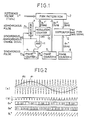
- Fig. 1 is a block diagram of a first embodiment of a PWM controller according to the present invention;
- Fig. 2 shows wave forms of signals for preparing a PWM signal for use in both synchronous and asynchronous PWM controls according to the present invention;
- Fig. 3 shows wave forms of signals for conducting the operation of the synchronous PWM control in the PWM controller of Fig. 1;
- Fig. 4 shows wave forms of signals for conducting the operation of the asnynchronous PWM control in the PWM controller of Fig. 1;
- Figs. 5 and 6 show output signals of a memory for explaining generation of irregular pulses in the asynchronous PWM control in the PWM controller of Fig. 1;
- Fig. 7 is a block diagram of a second embodiment of a PWM controller according to the present invention;
- Fig. 8 is a block diagram of a third embodiment of a PWM controller according to the present invention;
- Fig. 9 is a block diagram of a chattering stopper of the third embodiment of the controller shown in Fig. 8;
- Fig. 10 shows wave forms of signals in the chattering stopper shown in Fig. 9; and
- Fig. 11 is a schematic block diagram of a widely used inverter along with a PWM controller according to the present invention, which is applied thereto.
- Referring now to the drawings, wherein like reference characters designate like or corresponding parts throughout the several views, there is shown in Fig. 1 a first embodiment of a PWM controller according to the present invention.
- In the drawing, a plurality of PWM pattern data is stored in or read out of a
PWM pattern ROM 2, and a reference voltage V* is input to theROM 2 as a pattern selecting signal to address a PWM pattern address area of a certain voltage. First, second andthird phase counters ROM 2 and, in the same time, the PWM pattern data having the predetermined electrical angle is addressed. In this embodiment, a pulse signal having a frequency proportional to an operating frequency of an inverter to which the PWM controller of the present invention is applied, is given as the synchronous pulse P₁ to thefirst phase counter 4, as hereinafter described in detail. - In this embodiment, for instance, the reference voltage V* and the counted values ϑL*, ϑM* and ϑH* of the first, second and
third phase counters - The
phase counter 6 is a hexadic counter to output six values ϑH* such as 0 to 5. Theother counters selector 7 along with the synchronous pulses P₁, and theselector 7 selects the synchronous pulses P₁ or the asynchronous pulses P₂ according to a synchronous/asynchronous change signal MS as a mode signal to be fed to theselector 7 and outputs the selected pulses P₁ or P₂ to amodulation counter 10. Themodulation counter 10 counts the number of the pulses P₁ or P₂ and sends the counted value ϑL*′ of 6 bits to theROM 2. Thebit number 6 of the counted value ϑL*′ of themodulation counter 10 is the same as that of thefirst phase counter 4. The mode signal MS is supplied to anAND circuit 11 where, when the mode signal MS selects the synchronous pulse P₁, its gate is opened to pass a carry CRY of the themodulation counter 10 to thefirst phase counter 4, and the carry CRY clears the count number to naught in thefirst phase counter 4. Thesecond phase counter 5 outputs the counted value ϑM* to theROM 2. - The
ROM 2 is addressed by the code of 15 bits, i.e., the reference V*, the counted value ϑL*′ of themodulation counter 10 and the counted value ϑM* of thesecond phase counter 5 to output the stored PWM pattern data as signals Qout of 6 bits to adistributor 12. For information, a device interchangeable with PROMi-27256 (Trade Name) of INTER CORPORATION is provided with an 8-bit data line, and its 6 bits may be used for theROM 2. - The 6-bit PWM data Qout is fed from the
ROM 2 to adistributor 12, and thedistributer 12 selects 3-bit data from the 6-bit PWM data Qout and outputs the selected 3-bit PWM pattern data as PWM control signals Pout for three phases of a three-phase inverter. The 3-bit counted value ϑH* is also input from thethird phase counter 6 to thedistributer 12 for instructing the above data distribution operation. - The 6-bit PWM Qout output simultaneously from the
ROM 2 includes 6 data having a period of 60° and a phase difference of 60° which is obtained by dividing one period of its periodic function into six equal parts. - Assuming that the periodic function is represented by a sine wave, the PWM data will be described in connection with Fig. 2.
- Fig. 2a illustrates a sine wave e₁ having an amplitude V* and a triangular wave e₂ having a constant amplitude, and Fig. 2b shows a PWM signal obtained by comparing these two signals e₁ and e₂. The frequency of the triangular wave e₂ is set to 24 times of the frequency of the sine wave e₁, and this 24 number is determined by, e.g., 6x4=24, wherein 6 stands on 6 bits of the output data Qout of the
ROM second phase counter 5. The frequency of the triangular wave e₂ may be determined to integral times, e.g., twice, three times or four times of 24. - Concerning the logical values of the PWM signal shown in Fig. 2b, the sine wave PWM signal having the amplitude V* is obtained by setting continuity periods of positive and negative side elements of an inverter bridge to "1" and "0", respectively.
- One cycle of sine wave PWM signal shown in Fig. 2b is divided into six equal parts by the period of 60°, and thus is stored as six PWM pattern data having periods 0 - 60°, 60 - 120°, 120 - 180°, 180 - 240°, 240 - 300° and 300 - 360° in 0-bit, 1-bit, 2-bit, 3-bit, 4-bit and 5-bit of the
ROM 2. Accordingly, the six PWM pattern data having the phase difference 60° from one another are simultaneously and repeatedly read out of theROM 2 by the counted value ϑL*′ of thefirst phase counter 4 and the counted value ϑM* of thesecond phase counter 5, and thedistributor 12 changes consecutively the bits every 60° period by the counted value ϑH* of thethird phase counter 6 to output one cycle of the PWM pattern data as the PWM control signals Pout. - The PWM pattern data of Fig. 2b is obtained by continuously changing 0-bit, 1-bit, 2-bit, 3-bit, 4-bit and 5-bit of the
ROM 2 using the counted value ϑH* of thethird phase counter 6. In this embodiment, since the frequency of the triangular wave e₂ is determined to 24 times of that of the sine wave e₁, the period of the counted value ϑL* of thefirst phase counter 4 is equal to that of the triangular wave e₂. - Then, the operation of the synchronous PWM control according to the present invention will now be described in connection with Fig. 3.
- The first, second and third phase counters always count the synchronous pulses P₁, and the relation among their counted values ϑL*, ϑM* and ϑH* is shown in Fig. 3. In the synchronous PWM control, the synchronous/asynchronous change signal MS becomes "1", and the
selector 7 selects the synchronous pulses P₁. Hence, the counted value ϑL*′ of themodulation counter 10 becomes equal to the counted value ϑL* of thefirst phase counter 4. Even when the counted value ϑL* temporarily becomes different from the counted value ϑL*′, themodulation counter 10 outputs the carry CRY to theAND circuit 11, and thefirst phase counter 4 is cleared by the carry CRY passing through theAND circuit 11. Then, the counted values of thefirst phase counter 4 and themodulation counter 10 are simultaneously cleared to naught by the next synchronous pulse P₁, and thereafter the counted values ϑL* and ϑL*′ of the twocounters - The
ROM 2 outputs the 6-bit PWM pattern data e₀ to e₅ stored in the addresses addressed by the reference voltage V* and the counted values ϑM* and ϑL*′ of themodulation counter 10 and thesecond phase counter 5, as the Qout signal to thedistributor 12. As the counted value ϑH* of thethird phase counter 6 varies every one cycle such as 0 → 1 → 2 → 3 → 4 → 5 → 0, thedistributor 12 changes the 3-bit PWM control signal Pout so as to selectively output the PWM data, e.g., e₀ → e₁ → e₂ → e₃ → e₄ → e₅ → e₀ for U-phase, e₄ → e₅ → e₀ → e₁ → e₂ → e₃ → e₄ for V-phase or e₂ → e₃ → e₄ → e₅ → e₀ → e₁ → e₂ for W-phase. The output data Pout for the U-, V- and W-phases have the same wave form as the PWM pattern data shown in Fig. 2b, except their phase differences of 120°, and thus may be used symmetrical three phase PWM signals. - Then, the operation of the asynchronous PWM control according to the present invention will be described with reference to Fig. 4.
- In this case, the synchronous/asynchronous change signal MS is set to "0", and the
selector 7 selects the asynchronous pulses P₂. Thus, the counted value ϑL*′ of themodulation counter 10 is advanced by the asynchronous pulses P₂, and the counted values ϑL*, ϑM* and ϑH* of the first, second and third phase counters 4, 5 and 6 are forwarded by the synchronous pulses P₁. Further, since the synchronous/asynchronous change signal MS becomes "0", even when themodulation counter 10 outputs the carry CRY, thefirst phase counter 4 is not cleared. That is, in this embodiment, themodulation counter 10 is completely isolated in operation from the first, second and third phase counters, 4, 5 and 6. - In Fig. 4, the frequency f₂ of the asynchronous pulses P₂ is determined to approximately 1.4 times of the frequency f₁ of the synchronous pulses P₁. Accordingly, in this case, one period or cycle (t₀ to t₁) of the counted value ϑL*′ of the
modulation counter 10 is 1/1.4 (approximately 70%) of one cycle (t₀ to t₂) of the counted value ϑL* of thefirst phase counter 4. Hence, as to the output pattern data Qout of theROM 2, the phase width is compressed to approximately 70% in comparison with the one shown in Fig. 3. The counted value ϑL*′ of themodulation counter 10 is reset to "0" at the time t₁, and themodulation counter 10 starts again to count the pulses. However, while the counted value ϑM* of thesecond phase counter 5 is not changed in the period (t₁ to t₂), the pattern data is output again from theROM 2 in the period (t₀ to t₁). - Now, when f₂/f₁ is defined to n, the pattern data in the period (t₀ to t₁) is repeatedly output n times. Since f₂/f₁ is 1.4 in the embodiment of Fig. 4, the pattern data in the period (t₁ to t₂) corresponding to the former 40% of the pattern data in the period (t₀ to t₁) is output.
- The counted value ϑL* of the
first phase counter 4 for counting the number of the synchronous pulses P₁ overflows at a time t₂ to advance the counted value ϑM* of thesecond phase counter 5 from "0" to "1" while themodulation counter 10 independently continues counting of the asynchronous pulses P₂. - Accordingly, the pattern data output from the
ROM 2 in the period (t₂ to t₃) corresponds to approximately the latter 60% of the pattern data shown in Fig. 3, which is output from theROM 2 during the period of 0H*=0 to 0M*=1 in the synchronous PWM mode, while the phase width of the output pattern data is compressed to approximately 70% of the pattern data of Fig. 3 in the same time, like the data e₀ to e₅ shown in Fig. 4. - As described above, in Fig. 4, the pattern data e₀ to e₅ output from the
ROM 2 in the period (t₁ to t₃) becomes a combination of the pattern data of Fig. 3 during the period ϑH*=0 to ϑM*=0 and the pattern data of Fig. 3 during the period ϑH*=0 to 0M*=1 at the ratio of approximately 4:6, and the phase widths of the pattern data e₀ to e₅ are compressed to approximately 70% of those shown in Fig. 3 - Then, the pattern data of e₀ to e₅ shown in Fig. 4 is read out of the
ROM 2 in the same manner as described above, and thedistributer 12 outputs the 3-phase PWM signals Pout for the U-, V- and W-phases by the counted value ϑH* of thethird phase counter 6 in the same manner as the synchronous PWM mode described above. As shown in Fig. 4, the PWM signals each include one pulse having a different width therefrom per one cycle of the counted value ϑL*′ of themodulation counter 10, and act as the asynchronous PWM control signals whose pulse width modulation frequencies can be determined by the frequency f₂ of the asynchronous pulses P₂. - As described above, the synchronous PWM control and the asynchronous PWM control are changed by setting the synchronous/asynchronous change signal MS to "1" or "0", and the PWM pattern data to be stored in the
ROM 2 must be synchronous/asynchronous common-use pattern data including an integral number of pulses per one cycle of the counted values ϑM* of thesecond phase counter 5, as shown in Fig. 2, so as not to generate an excessive and irregular pulse having a narrow width in the asynchronous PWM control. However, in a high voltage and high frequency region where only the synchronous PWM control is conducted, various PWM pattern data may be stored at will in theROM 2. Hence, the synchronous/asynchronous common-use pattern data may be used only in the asynchronous PWM control region. - Even when the counted value ϑL*′ of the
modulation counter 10 is different from the counted value ϑL* of thefirst phase counter 4 on changing from the asynchronous PWM control to the synchronous PWM control, as soon as outputting the carry CRY from themodulation counter 10, thefirst phase counter 4 is cleared by the next synchronous pulse P₁, resulting in that the counted value ϑL* of thefirst phase counter 4 becomes equal to the counted value ϑL*′ of themodulation counter 10. That is, thefirst phase counter 4 is cleared by the synchronous pulse P₁ only after the outputting of the one pulse is finished, and therefore no irregular pulse is produced when the asynchronous PWM control is changed to the synchronous PWM control. Further, at this asynchronous to synchronous change time, the voltage phase of at most one cycle of thefirst phase counter 4 is jumped. - Although one cycle of the
first phase counter 4 is determined to 15° in this embodiment, when the bit number of thefirst phase counter 4 and themodulation counter 10 is reduced in order to decrease one cycle, for example, to 7.5 or 3.75 while the bit number of thesecond phase counter 5 is enlarged, the jumped amount on changing the asynchronous PWM control to the synchronous PWM control is reduced to obtain a smooth change operation. Further, although the PWM pattern data of one cycle of the sine wave is entirely stored in theROM 2 in this embodiment, by utilizing the symmetrical nature of the wave forms, only one fourth period (0 to 90°) of the PWM pattern data may be stored in theROM 2, and the PWM pattern data may be repeatedly read out of theROM 2 to produce one cycle of the PWM pattern data. - In this embodiment, the change from the synchronous PWM control to the asynchronous PWM control can be readily and smoothly carried out without any trouble because the counted values of the
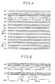
first phase counter 4 and themodulation counter 10 are equal at the changing moment. - Now, the generation of the irregular pulse in the asynchronous PWM control will be described.
- Fig. 5 shows a PWM pattern signal Qout output from the
ROM 2 in the synchronous PWM control and Fig. 6 shows another PWM pattern signal Qout having irregular pulses therein in the asynchronous PWM control with respect to the counted values ϑL*, ϑM* and ϑL*′ of the first andsecond phase counter modulation counter 10, in which thefirst phase counter 4 and themodulation counter 10 are assumed to be 3 bits for the brevity of the description. - In the synchronous PWM control, as shown in Fig. 5, the counted value ϑL*′ of the
modulation counter 10 becomes equal to the counted value ϑL* of thefirst phase counter 4, and the PWM pattern data stored in theROM 2 is read out of theROM 2 as the output PWM pattern data Qout as it is. In the asynchronous PWM control, in turn, as shown in Fig. 6, the frequency f₂ of the asynchronous pulse P₂ is somewhat higher than that f₁ of the synchronous pulse P₁, and the counted value ϑL*′ of themodulation counter 10 is counted somewhat faster than that ϑL* of thefirst phase counter 4. - That is, the
modulation counter 10 counts up the full count in the period (t₀ to t₁) and one cycle of the PWM pattern data corresponding to the PWM pattern data during the time of the counted value ϑM*=n in Fig. 5 is output from theROM 2, and theROM 2 repeatedly sends out the same PWM pattern data until the counted value ϑM* of thesecond phase counter 5 becomes n+1 at the time t₃. Accordingly, the output Qout of theROM 2 becomes "0" at the time t₂ when the counted value ϑL*′ of themodulation counter 10 becomes "1". When the counted value ϑM* of thesecond phase counter 5 is changed to n+1 at the time t₃, theROM 2 outputs a next cycle of PWM pattern data from the phase of the counted value ϑL*′=1, and the output Qout of theROM 2 becomes "1". Then, theROM 2 repeatedly outputs a second cycle of PWM pattern data corresponding to the PWM pattern data during the time of the counted value ϑM*=n+1 in Fig. 5, according to the counted value ϑL*′ of themodulation counter 10 in the period (t₃ to t₈). Hence, the output Qout of theROM 2 changes, such as "0" at the time t₄ when the counted value ϑL*′ of themodulation counter 10 becomes "2", "1" at the time t₅ when the counted value ϑL*′ is "6", and "0" at the time t₇ when the counted value ϑL*′ is "2". Then, the PWM pattern data is output from theROM 2 according to the asynchronous pulses P₂ in the same manner as described above. - The asynchronous PWM pattern data having two pulses per one cycle of the
modulation counter 10 in the period (t₁ to t₆), as shown in Fig. 6, has an irregular pulse wave form with respect to that of Fig. 5. The duty factor of the asynchronous PWM pattern data Qout in the period (t₁ to t₆) of Fig. 6 is an intermediate between the duty factors of the synchronous PWM pattern data in the periods of ϑM=n and ϑM=n+1 of Fig. 5, and is closer to the latter rather than the former, and the wave form of the asynchronous PWM pattern data in the period (t₁ to t₆) may be considered to be a right wave form. Therefore, when switching elements having excellent characteristics such as a very high operation speed and a very small loss are used, this asynchronous PWM pattern data may be used actually as it is. - However, in practice, as the operation speed of the switching elements increases, the modulation is usually performed at a higher frequency, and thus it is not desirable to increase the switching times more than a certain number of times by using the PWM pattern data shown in Fig. 6.
- In Fig. 7, there is shown a second embodiment of a PWM controller according to the present invention, which is capable of preventing the generation of the irregular pulses of the first embodiment described above.
- In this embodiment, the PWM controller has the same construction as that of the first embodiment, except a
latch circuit 13 for once latching the PWM control signals output from thedistributor 12 in accordance with the pulse output from theselector 7. That is, in the asynchronous PWM control, when the output data Qout shown in Fig. 6 is output as the PWM signal from thedistributor 12, the PWM pattern data which is the output data just before the counted value ϑL*′ of themodulation counter 10 is advanced by the asynchronous pulse P₂ and is latched in thelatch circuit 13, is output therefrom. Hence, the "0" periods (t₂ to t₃) and (t₇ to t₈) of the output data Qout shown in Fig. 6 can be omitted. In this embodiment, however, such "0" period omissions can be made only when the difference between the leading and trailing addresses (the counted values ϑL*) of the PWM pattern data in the adjacent two counted values ϑM* of thesecond phase counter 5, is "1" or "0", and, when the difference between the leading and trailing addresses is more than "1", the irregular pulses may be produced, as shown in Fig. 6. In the three-phase sine wave PWM pattern data, the output data may be continuously changed, and the bit numbers of the first and second phase counters 4 and 5 and themodulation counter 10 may be selected so as to satisfy the above described "0" period omission conditions. - In Fig. 8, there is shown a third embodiment of a PWM controller according to the present invention, which is capable of preventing the production of the irregular pulses of the first embodiment.
- In this embodiment, a chattering
stopper 14 for preventing the production of the irregular pulses is additionally provided between theROM 2 and thedistributor 12, as compared with the first embodiment. The chatteringstopper 14 removes the irregular pulses in the PWM pattern data Qout output from theROM 2 according to the uppermost bit S of the counted value ϑL*′ of themodulation counter 10. One embodiment of the chatteringstopper 14 is shown in Fig. 9. - In Fig. 9, the chattering
stopper 14 includes sixpulse reforming circuits 20a to 20f for one bit and aNOT circuit 21. Each of the pulse reforming circuits 20 to 20f having the same construction and functions includes aNOT circuit 22, four ANDcircuits circuit 25 and a flip-flop circuit 26. Thepulse reforming circuits 20a to 20f reform the PWM pattern data e₀ to e₅, respectively, using the uppermost bit S of the counted value ϑL*′ of themodulation counter 10 to output reformed data PS0 to PS5, respectively, to thedistributor 12. Thus, the operation of one of thepulse reforming circuits 20a to 20f will be described in detail in connection with Fig. 10. - In Fig. 10, one PWM pattern data e₀ including irregular pulses, output from the
ROM 2, will be reformed to the data PS0 by using the uppermost bit S of the counted value ϑL*′ of themodulation counter 10, as follows. That is, the two signals e₀ and S are logically synthesized by the twoNOT circuits circuits circuit 25 to obtain a signal CP, as shown in Fig. 10, which is fed as a clock signal to the flip-flop circuit 26. Logical products of the signals S andS and output signalsQ and Q (PS0 and PS0) of the flip-flop circuit 26 are input as signals DJ and DK to input terminals J and K of the flip-flop circuit 26 through the ANDcircuits - Now, when the output signal PS0 of the flip-
flop circuit 26 is "1" at the time t₀ and the uppermost bit S of the counted value ϑL*′ of themodulation counter 10 is "0", the input signals DJ and DK of the flip-flop circuit 26 becomes "0" and "1", respectively. The signals DJ and DK are input to the flip-flop circuit 26 when the clock signal CP is "0", and, when the clock signal CP then rises to "1" at the time t₁, the output signal PS0 is changed to "0". Then, the input signal DK is also changed to "0". In turn, since the signal S is still kept to "0", the input signal DJ is also "0". Therefore, since the input signals DJ and DK are "0", the flip-flop circuit 26 is in the restrained state and is not changed by the clock signal CP. Even when the clock signal CP is changed to "0" or "1" at the time t₂ or t₃, the output signal PS0 is not changed to be "0". Then, when the signal S becomes "1" at the time t₄, the input signal DJ of the flip-flop circuit 26 is changed to "1", and the output signal PS0 of the flip-flop circuit 26 may be changed to "1" by the clock signal CP. Hence, when the clock signal CP is changed from "0" to "1" at the time t₅, the output signal PS0 of the flip-flop circuit 26 is changed from "0" to "1". When the output signal PS0 of the flip-flop circuit 26 is changed to "1", the input signal DJ of the flip-flop circuit 26 is changed to "0" to change the flip-flop circuit 26 to the restrained state again. Then, when the signal S becomes "0" at the time t₆, the input signal DK is changed to "1", and the output signal PS0 of the flip-flop circuit 26 becomes "1" again in the same state as the time t₀ described above. The same operation as described above will be repeated. - As described above, the irregular pulses included in the signal e₀ output from the
ROM 2 is removed in thepulse reforming circuit 20a, and the signal PS0 including only one pulse per one cycle of themodulation counter 10 is output from thepulse reforming circuit 20a, and the modulation frequency becomes constant. Further, the duty factor of the output signal PS0 of thepulse reforming circuit 20a becomes an intermediate value between those of the output signals of theROM 2 when the counted values ϑM* of thesecond phase counter 5 are n and n+1. - In this embodiment, the output signal PS0 is allowed once to change from "1" to "0" in the former half of one cycle of the
modulation counter 10, and is also allowed once to change from "0" to "1" in the latter half of the one cycle of themodulation counter 10, thereby removing the irregular pulses, because of the PWM pattern data stored in theROM 2 changes "1" → 0 → "1" in one cycle of the synchronous control, as shown in Fig. 2b. In turn, when the PWM pattern data is stored oppositely in theROM 2 such as "0" → "1" → "0", the output signal PS0 may be allowed once to change from "0" to "1" in the former half of one cycle of themodulation counter 10 and also be allowed once change from "1" to "0" in the latter half of the one cycle of themodulation counter 10 in thepulse reforming circuits 20a to 20f. - In the third embodiment shown in Fig. 8, the limited conditions of the PWM pattern data in the second embodiment shown in Fig. 6 are unnecessary, and, even when the difference between the leading and training addresses of th PWM pattern data in the adjacent two counted values ϑM* of the
second phase counter 5 is more than one, the irregular pulses may be removed as described above. Accordingly, in addition to the three-phase sine wave PWM pattern data, the present invention may be applied to two-phase sine wave PWM pattern data (one phase is fixed to a certain positive or negative voltage and only the other two phases are controlled to control the voltages among the three phases to approximate sine waves). Although the chatteringstopper 14 is positioned between theROM 2 and thedistributor 12 in the third embodiment, the chatteringstopper 14 may be placed in the output side of thedistributor 12 to output the PWM control pattern data, and, in this case, it requires only three pulse reforming circuits, which is economical and simple in construction. - In the above described preferred embodiments, the
first phase counter 4 is cleared by the carry CRY of themodulation counter 10 in the synchronous PWM control in order to prevent the overcurrent since a pulse having a wider width than that in the normal operation when the synchronous PWM control is changed to the asynchronous PWM control. However, when the PWM control is conducted at more than 10 KHz using a quick switching elements such as FET devices, the current ripple is quite small, and hence themodulation counter 10 may be cleared by the carry CRY of thefirst phase counter 4 in the synchronous PWM control. In such a case, when the asynchronous PWM control is changed to the synchronous PWM control, the pulse having a wide width is produced, but its influence is very small. Further, there is no phase jump when the change between the synchronous and asynchronous PWM controls is carried out. - Further, when there is sufficient capacity in the
ROM 2, both in the synchronous PWM pattern data and the synchronous/asynchronous common use PWM pattern data may be stored in theROM 2, and one of them may be selected by the synchronous/asynchronous change signal MS. In the synchronous PWM control, the modulation frequency of the PWM pattern data varies depending on the output frequency of the inverter. However, the modulation frequency does not vary in the asynchronous PWM control, and it may be advantageous to select the asynchronous PWM control in a certain voltage depending on noisy or other operational conditions. In these cases, the synchronous/asynchronous changes can be carried out regardless of the reference voltage V*. - As described above, in the preferred embodiments of the present invention, when the value ϑL*′ of the modulation counter is counted by the frequency proportional to the operational frequency to obtain the same value as the lower bit ϑL* of the first phase counter, the PWM pattern data read out of the memory becomes the pattern addressed by the intermediate and lower bits (electrical angles ϑM* + ϑL*) of the first and second phase counters, and this pattern data is distributed by the higher bit value ϑH* of the third phase counter, thereby operating in the synchronous PWM control which is capable of outputting the optimum pattern data stored in the memory.
- When the modulation counter is counted by a constant frequency, the frequency of the counted value ϑL*′ of the modulation counter becomes different from that of the lower bit value ϑL* of the first phase counter. When the frequency for counting the modulation counter is high, the modulation counter is repeatedly counted in some cycles to repeatedly output the same value ϑL*′ during the time of the constant value ϑM* to be fed to the memory. Hence, until one cycle of the lower bit value ϑL* of the first phase counter is counted and the intermediate value ϑM* of the second phase counter is changed, many pulses are output from the modulation counter, and their frequency is determined by the frequency for counting the modulation counter, i.e., to operate in the asynchronous PWM control.
- There is shown in Fig. 11 a widely used inverter along with a PWM controller according to the present invention, which is applied thereto. In Fig. 11, a three-phase
commercial power source 30 is connected to arectifier 31 for rectifying an alternating voltage into a direct voltage, and acapacitor 32 is coupled to therectifier 31 in parallel therewith. Aninverter 33 for converting a direct voltage into an alternating voltage is connected to therectifier 31 and thecapacitor 32 in parallel therewith, and a three-phase induction motor 34 is connected to theinverter 33. - A
frequency settler 35 for setting up the fundamental frequency of the alternating voltage output by theinverter 33 is connected to a voltage-frequency (V/F)converter 36, acomparator 38 and afunction generator 40. The V/F converter 36 outputs the synchronous pulses P₁ in proportion to the output voltage of thefrequency settler 35 to thePWM controller 37 according to the present invention. When the output voltage of thefrequency settler 35 is more than or at most a predetermined voltage, thecomparator 38 outputs a logical value "1" or "0" as the synchronous/asynchronous change signal MS to thePWM controller 37, and anoscillator 39 generates a clock pulse having a certain frequency as the asynchronous pulse P₂ to thePWM controller 37. Thefunction generator 40 outputs the reference voltage V* to thePWM controller 37 through an analog-digital (A/D)converter 41. ThePWM controller 37 outputs the three-phase PWM control signals Pout for the U-, V- and W-phases to abase driver 43 directly or via threeNOT circuits base driver 43, and the amplified PWM control signals are fed to theinverter 33 for driving the corresponding switching elements therein. - In this applied case, the PWM pattern data such as a synchronous/asynchronous common use pattern data for use in a low voltage region and a synchronous exclusive use pattern data of a low-dimensional harmonic elimination PWM control system for use in a high voltage region is stored in the
ROM 2 within thePWM controller 37. When the output voltage of thefrequency settler 35 is smaller than the comparison level of thecomparator 38, the change signal MS selects the asynchronous pulses P₂, and thePWM controller 37 reads out the synchronous/asynchronous common use pattern data according to the asynchronous pulses P₂ output by theoscillator 39 to operate theinverter 33 in the asynchronous PWM control where the modulation frequency is constant. When thefrequency settler 35 is controlled so that the output voltage of thefrequency settler 35 is more than the comparison level of thecomparator 38, the change signal MS selects the synchronous pulses P₁, andPWM controller 37 reads out the synchronous/asynchronous common use pattern data according to the synchronous pulses P₁ output by the V/F converter 36 to operate theinverter 33 in the synchronous PWM control, in which the modulation frequency is proportional to the operating frequency. Then, when thefrequency settler 35 is controlled to further raise the output voltage, theROM 2 outputs the synchronous pattern data of the low-dimensional harmonic elimination PWM control system to operate theinverter 33 in the synchronous PWM control of the low-dimensional harmonic elimination PWM control system. - Accordingly, by using a memory having a limited capacity, the inverter may be operated in the asynchronous PWM control corresponding to the triangular wave comparison in the low speed region, in the synchronous PWM control corresponding to the triangular wave comparison in the intermediate speed region or in the synchronous PWM control of the low-dimensional harmonic elimination control system in the high speed region. Hence, the
inverter 33 can be operated in the optimum PWM control system depending on the frequency from the low speed region to the high speed region, and the low current ripple and the high efficient PWM control can be performed in the wide operational frequency range. - As described above, it is readily understood that according to the present invention it is possible to conduct an asynchronous PWM control by a PWM controller including a memory in which PWM pattern data is stored. Since a synchronous/asynchronous common use pattern data is prepared for the PWM pattern data corresponding to a triangular wave comparison, it is possible to conduct three PWM controls such as the asynchronous PWM control corresponding to the triangular wave comparison, the synchronous PWM control corresponding to the triangular wave comparison and the PWM control using the pattern data calculated in various conventional off-lines. Further, it is possible to carry out various PWM controls depending on the operational frequency and the output voltage, and the extension of the operational frequency range and the highly effective operation can be performed. Furthermore, the asynchronous PWM control can be conducted using the memory without providing a particular asynchronous PWM controller, the economical and widely used PWM controller can be provided.
- Although the present invention has been described in its preferred embodiments with reference to the accompanying drawings, it is readily understood that the present invention is not limited to the preferred embodiments, and various changes and modification of the present invention may be made by a person skilled in the art without departing from the spirit and scope of the present invention.
Claims (8)
phase counter means (4,5,6) for counting synchronous pulses having a proportional frequency to that of an inverter (33) to be controlled to output a phase signal;
memory means (2) for storing at least two PWM pattern data with addresses, the PWM pattern data being read out by addressing using a pattern selection signal and the phase signal;
distributor means (12) for distributing the PWM pattern data read out of the memory means (2) using upper bit of the phase signal to output PWM signals for controlling the inverter (33); and
modulation counter means (10) for counting one of the synchronous pulses and asynchronous pulses having a certain frequency to output a counted value to the memory means (2), the one of the synchronous and asynchronous pulses being selected according to a mode signal, the counted value of the modulation counter means (10) being used instead of lower bit of the phase signal to selectively output the PWM signals of one of synchronous and asynchronous PWM controls.
Applications Claiming Priority (2)
| Application Number | Priority Date | Filing Date | Title |
|---|---|---|---|
| JP62284217A JPH0681513B2 (en) | 1987-11-12 | 1987-11-12 | PWM controller |
| JP284217/87 | 1987-11-12 |
Publications (3)
| Publication Number | Publication Date |
|---|---|
| EP0316006A2 true EP0316006A2 (en) | 1989-05-17 |
| EP0316006A3 EP0316006A3 (en) | 1989-12-06 |
| EP0316006B1 EP0316006B1 (en) | 1993-05-19 |
Family
ID=17675683
Family Applications (1)
| Application Number | Title | Priority Date | Filing Date |
|---|---|---|---|
| EP88118835A Expired - Lifetime EP0316006B1 (en) | 1987-11-12 | 1988-11-11 | Pwm controller |
Country Status (6)
| Country | Link |
|---|---|
| US (1) | US4860186A (en) |
| EP (1) | EP0316006B1 (en) |
| JP (1) | JPH0681513B2 (en) |
| KR (1) | KR920004905B1 (en) |
| CN (1) | CN1010362B (en) |
| DE (1) | DE3881161T2 (en) |
Cited By (6)
| Publication number | Priority date | Publication date | Assignee | Title |
|---|---|---|---|---|
| WO1993023912A1 (en) * | 1992-05-11 | 1993-11-25 | Solar Turbines Incorporated | Programmed pwm inverter controller |
| AT401450B (en) * | 1989-10-09 | 1996-09-25 | Fronius Schweissmasch | Control method for three-phase bi-directional pulse converters with a high clock rate |
| WO2011120816A3 (en) * | 2010-03-31 | 2012-07-26 | Robert Bosch Gmbh | Method for driving an electric motor |
| EP2802067A1 (en) * | 2013-04-09 | 2014-11-12 | Hamilton Sundstrand Corporation | Lookup table assisted pulse width modulation |
| AT515243A1 (en) * | 2013-12-19 | 2015-07-15 | Schneider Electric Power Drives Gmbh | Method for controlling parallel-connected inverters |
| CN111656677A (en) * | 2018-03-16 | 2020-09-11 | 日立汽车系统株式会社 | Motor control device |
Families Citing this family (16)
| Publication number | Priority date | Publication date | Assignee | Title |
|---|---|---|---|---|
| DE69030701T2 (en) * | 1989-10-02 | 1997-10-02 | Canon Kk | Imaging device and modulation method |
| US5418932A (en) * | 1990-02-01 | 1995-05-23 | Hitachi, Ltd. | Generation of width modulated pulses by relatively adjusting rising and falling edges upon comparison of counter with programmably stored values |
| US4994950A (en) * | 1990-07-31 | 1991-02-19 | Eaton Corporation | Waveform generator for inverter control |
| US5506487A (en) * | 1991-03-28 | 1996-04-09 | General Electric Company | Systems and methods for driving a compressor with a motor |
| US5615099A (en) * | 1994-08-24 | 1997-03-25 | Kabushiki Kaisha Toshiba | Control system for single-phase PWM converter |
| DE19541832A1 (en) * | 1995-11-10 | 1997-05-15 | Thomson Brandt Gmbh | Motor control for electronically commutating direct current motors to compensate for torque drops |
| US5835363A (en) * | 1997-11-13 | 1998-11-10 | Acer Peripherals, Inc. | Power supply device featuring synchronous mode and asynchronous mode operation |
| US7049771B2 (en) * | 2004-01-27 | 2006-05-23 | Nippon Yusoki Co., Ltd. | Multi-phase carrier signal generator and multi-phase carrier signal generation method |
| US7049778B2 (en) * | 2004-02-09 | 2006-05-23 | Nippon Yusoki Co., Ltd. | Inverter control apparatus and inverter control method |
| FI118875B (en) * | 2006-09-26 | 2008-04-15 | Vacon Oyj | Parallel connection of inverters |
| EP2642658B1 (en) * | 2007-09-25 | 2018-08-29 | Mitsubishi Electric Corporation | Controller for electric motor |
| JP5253828B2 (en) * | 2008-01-25 | 2013-07-31 | ルネサスエレクトロニクス株式会社 | Motor driving device and semiconductor integrated circuit device |
| US8890457B2 (en) * | 2008-09-19 | 2014-11-18 | Hewlett-Packard Development Company, L.P. | Systems and methods for controlling motors |
| JP4858597B2 (en) | 2008-11-28 | 2012-01-18 | 株式会社デンソー | Rotating machine control device and manufacturing method thereof |
| US8345451B2 (en) * | 2009-11-08 | 2013-01-01 | Wernlund James V | DC to AC converter that generates the sine wave from the pulse width modulated signal |
| US20230308006A1 (en) * | 2022-03-24 | 2023-09-28 | Tae Technologies, Inc. | Communication systems and synchronization techniques for energy storage systems |
Citations (2)
| Publication number | Priority date | Publication date | Assignee | Title |
|---|---|---|---|---|
| US4356544A (en) * | 1980-06-05 | 1982-10-26 | Tokyo Shibaura Denki Kabushiki Kaisha | Apparatus for controlling an inverter main circuit |
| JPS592574A (en) * | 1982-06-25 | 1984-01-09 | Toshiba Corp | Current command value calculating system for power converter |
Family Cites Families (8)
| Publication number | Priority date | Publication date | Assignee | Title |
|---|---|---|---|---|
| US4099109A (en) * | 1976-10-01 | 1978-07-04 | Westinghouse Electric Corp. | Digital apparatus for synthesizing pulse width modulated waveforms and digital pulse width modulated control system |
| JPS6014693A (en) * | 1983-07-05 | 1985-01-25 | 松下電工株式会社 | Corrugated flexible pipe joint |
| JPH07108095B2 (en) * | 1984-01-20 | 1995-11-15 | 株式会社日立製作所 | Inverter device and control method thereof |
| JPH065989B2 (en) * | 1984-01-23 | 1994-01-19 | 富士電機株式会社 | Inverter PWM signal generator |
| JPS60174088A (en) * | 1984-02-17 | 1985-09-07 | Fanuc Ltd | Digital control system of ac motor |
| JPS62118774A (en) * | 1985-11-18 | 1987-05-30 | Toshiba Corp | Pulse width modulation signal generation system for inverter |
| JPH07112360B2 (en) * | 1986-07-25 | 1995-11-29 | 株式会社日立製作所 | Control method and apparatus for PWM inverter |
| JPH0779551B2 (en) * | 1987-03-20 | 1995-08-23 | 株式会社日立製作所 | Inverter control device |
-
1987
- 1987-11-12 JP JP62284217A patent/JPH0681513B2/en not_active Expired - Lifetime
-
1988
- 1988-11-08 US US07/268,567 patent/US4860186A/en not_active Expired - Fee Related
- 1988-11-11 EP EP88118835A patent/EP0316006B1/en not_active Expired - Lifetime
- 1988-11-11 DE DE88118835T patent/DE3881161T2/en not_active Expired - Fee Related
- 1988-11-12 CN CN88107833A patent/CN1010362B/en not_active Expired
- 1988-11-12 KR KR1019880014880A patent/KR920004905B1/en not_active IP Right Cessation
Patent Citations (2)
| Publication number | Priority date | Publication date | Assignee | Title |
|---|---|---|---|---|
| US4356544A (en) * | 1980-06-05 | 1982-10-26 | Tokyo Shibaura Denki Kabushiki Kaisha | Apparatus for controlling an inverter main circuit |
| JPS592574A (en) * | 1982-06-25 | 1984-01-09 | Toshiba Corp | Current command value calculating system for power converter |
Non-Patent Citations (1)
| Title |
|---|
| PATENT ABSTRACTS OF JAPAN, vol. 8, no. 81 (E-238)(1518) 13 April 1984; & JP-A-59 002 574 (TOKIO SHIBAURA DENKI) 9 January 1984. * |
Cited By (11)
| Publication number | Priority date | Publication date | Assignee | Title |
|---|---|---|---|---|
| AT401450B (en) * | 1989-10-09 | 1996-09-25 | Fronius Schweissmasch | Control method for three-phase bi-directional pulse converters with a high clock rate |
| WO1993023912A1 (en) * | 1992-05-11 | 1993-11-25 | Solar Turbines Incorporated | Programmed pwm inverter controller |
| WO2011120816A3 (en) * | 2010-03-31 | 2012-07-26 | Robert Bosch Gmbh | Method for driving an electric motor |
| CN102812630A (en) * | 2010-03-31 | 2012-12-05 | 罗伯特·博世有限公司 | Method for driving an electric motor |
| US9030138B2 (en) | 2010-03-31 | 2015-05-12 | Robert Bosch Gmbh | Method for driving an electric motor |
| CN102812630B (en) * | 2010-03-31 | 2016-06-15 | 罗伯特·博世有限公司 | Method for excited electric motor |
| EP2802067A1 (en) * | 2013-04-09 | 2014-11-12 | Hamilton Sundstrand Corporation | Lookup table assisted pulse width modulation |
| US9768755B2 (en) | 2013-04-09 | 2017-09-19 | Hamilton Sundstrand Corporation | Lookup table assisted pulse width modulation |
| AT515243A1 (en) * | 2013-12-19 | 2015-07-15 | Schneider Electric Power Drives Gmbh | Method for controlling parallel-connected inverters |
| CN111656677A (en) * | 2018-03-16 | 2020-09-11 | 日立汽车系统株式会社 | Motor control device |
| CN111656677B (en) * | 2018-03-16 | 2023-12-15 | 日立安斯泰莫株式会社 | Motor control device |
Also Published As
| Publication number | Publication date |
|---|---|
| EP0316006B1 (en) | 1993-05-19 |
| KR920004905B1 (en) | 1992-06-22 |
| CN1033134A (en) | 1989-05-24 |
| EP0316006A3 (en) | 1989-12-06 |
| US4860186A (en) | 1989-08-22 |
| DE3881161T2 (en) | 1993-10-21 |
| CN1010362B (en) | 1990-11-07 |
| DE3881161D1 (en) | 1993-06-24 |
| JPH0681513B2 (en) | 1994-10-12 |
| JPH01129774A (en) | 1989-05-23 |
| KR890009064A (en) | 1989-07-15 |
Similar Documents
| Publication | Publication Date | Title |
|---|---|---|
| EP0316006B1 (en) | Pwm controller | |
| EP0593738B1 (en) | Programmed pwm inverter controller | |
| EP0086650B1 (en) | Apparatus for providing a controlled power waveform | |
| US4599685A (en) | Control circuit for power converter apparatus | |
| US4656572A (en) | PWM inverter | |
| EP0469873A2 (en) | Waveform generator for inverter control | |
| US6548984B2 (en) | Power output device | |
| EP0371442A1 (en) | Control method of pulse width modulation inverter and pulse width modulation inverter system | |
| EP0077836B1 (en) | Control apparatus for electric motors | |
| US4352154A (en) | Varying two phase voltages in dc to three phase converter | |
| EP0467694B1 (en) | Three-phase PWM signal generating device for inverters | |
| US4924168A (en) | Control apparatus for PWM-controlled, variable voltage/variable frequency inverters | |
| JPH09182452A (en) | Three-level inverter | |
| JPS58127592A (en) | Controlling inverter for motor | |
| GB2125239A (en) | A three phase supply synthesis arrangement | |
| GB2171266A (en) | PWM inverter | |
| US4688163A (en) | Method for controlling the phase angle of the output current or the output voltage of a frequency converter and apparatus for carrying out the method | |
| JPH0447553B2 (en) | ||
| JPS6159062B2 (en) | ||
| JPH06178593A (en) | Variable speed driver of motor | |
| KR940007971B1 (en) | Room air conditioner inverter controlling method | |
| JPS6285678A (en) | Control circuit for inverter | |
| KR19990042262A (en) | Induction motor control method and control inverter | |
| JPH08214555A (en) | Method and apparatus for pulse-width-modulating three-phase voltage type inverter | |
| JPS61177174A (en) | Controller of inverter |
Legal Events
| Date | Code | Title | Description |
|---|---|---|---|
| PUAI | Public reference made under article 153(3) epc to a published international application that has entered the european phase |
Free format text: ORIGINAL CODE: 0009012 |
|
| 17P | Request for examination filed |
Effective date: 19881111 |
|
| AK | Designated contracting states |
Kind code of ref document: A2 Designated state(s): DE FR GB |
|
| PUAL | Search report despatched |
Free format text: ORIGINAL CODE: 0009013 |
|
| AK | Designated contracting states |
Kind code of ref document: A3 Designated state(s): DE FR GB |
|
| RHK1 | Main classification (correction) |
Ipc: H02M 7/5387 |
|
| 17Q | First examination report despatched |
Effective date: 19920115 |
|
| GRAA | (expected) grant |
Free format text: ORIGINAL CODE: 0009210 |
|
| AK | Designated contracting states |
Kind code of ref document: B1 Designated state(s): DE FR GB |
|
| REF | Corresponds to: |
Ref document number: 3881161 Country of ref document: DE Date of ref document: 19930624 |
|
| ET | Fr: translation filed | ||
| PLBE | No opposition filed within time limit |
Free format text: ORIGINAL CODE: 0009261 |
|
| STAA | Information on the status of an ep patent application or granted ep patent |
Free format text: STATUS: NO OPPOSITION FILED WITHIN TIME LIMIT |
|
| 26N | No opposition filed | ||
| PGFP | Annual fee paid to national office [announced via postgrant information from national office to epo] |
Ref country code: GB Payment date: 19941101 Year of fee payment: 7 |
|
| PGFP | Annual fee paid to national office [announced via postgrant information from national office to epo] |
Ref country code: FR Payment date: 19951109 Year of fee payment: 8 |
|
| PG25 | Lapsed in a contracting state [announced via postgrant information from national office to epo] |
Ref country code: GB Effective date: 19951111 |
|
| PGFP | Annual fee paid to national office [announced via postgrant information from national office to epo] |
Ref country code: DE Payment date: 19951113 Year of fee payment: 8 |
|
| GBPC | Gb: european patent ceased through non-payment of renewal fee |
Effective date: 19951111 |
|
| PG25 | Lapsed in a contracting state [announced via postgrant information from national office to epo] |
Ref country code: FR Effective date: 19970731 |
|
| PG25 | Lapsed in a contracting state [announced via postgrant information from national office to epo] |
Ref country code: DE Effective date: 19970801 |
|
| REG | Reference to a national code |
Ref country code: FR Ref legal event code: ST |