EP0309447B1 - Ciphering and deciphering device - Google Patents
Ciphering and deciphering device Download PDFInfo
- Publication number
- EP0309447B1 EP0309447B1 EP86903695A EP86903695A EP0309447B1 EP 0309447 B1 EP0309447 B1 EP 0309447B1 EP 86903695 A EP86903695 A EP 86903695A EP 86903695 A EP86903695 A EP 86903695A EP 0309447 B1 EP0309447 B1 EP 0309447B1
- Authority
- EP
- European Patent Office
- Prior art keywords
- code
- bits
- shift register
- input
- memory
- Prior art date
- Legal status (The legal status is an assumption and is not a legal conclusion. Google has not performed a legal analysis and makes no representation as to the accuracy of the status listed.)
- Expired - Lifetime
Links
- 230000015654 memory Effects 0.000 claims abstract description 78
- 230000005540 biological transmission Effects 0.000 description 27
- 239000000872 buffer Substances 0.000 description 6
- 238000010586 diagram Methods 0.000 description 6
- 230000000295 complement effect Effects 0.000 description 3
- 238000000034 method Methods 0.000 description 3
- 230000001360 synchronised effect Effects 0.000 description 3
- 230000006870 function Effects 0.000 description 2
- 238000012986 modification Methods 0.000 description 2
- 230000004048 modification Effects 0.000 description 2
- 230000000737 periodic effect Effects 0.000 description 2
- 229910000831 Steel Inorganic materials 0.000 description 1
- 230000004075 alteration Effects 0.000 description 1
- 230000003139 buffering effect Effects 0.000 description 1
- 238000004891 communication Methods 0.000 description 1
- 230000001934 delay Effects 0.000 description 1
- 230000001419 dependent effect Effects 0.000 description 1
- 238000013461 design Methods 0.000 description 1
- 230000000977 initiatory effect Effects 0.000 description 1
- 238000013507 mapping Methods 0.000 description 1
- 238000010079 rubber tapping Methods 0.000 description 1
- 239000010959 steel Substances 0.000 description 1
- 238000012546 transfer Methods 0.000 description 1
Images


Classifications
-
- H—ELECTRICITY
- H04—ELECTRIC COMMUNICATION TECHNIQUE
- H04L—TRANSMISSION OF DIGITAL INFORMATION, e.g. TELEGRAPHIC COMMUNICATION
- H04L9/00—Cryptographic mechanisms or cryptographic arrangements for secret or secure communications; Network security protocols
- H04L9/06—Cryptographic mechanisms or cryptographic arrangements for secret or secure communications; Network security protocols the encryption apparatus using shift registers or memories for block-wise or stream coding, e.g. DES systems or RC4; Hash functions; Pseudorandom sequence generators
- H04L9/065—Encryption by serially and continuously modifying data stream elements, e.g. stream cipher systems, RC4, SEAL or A5/3
-
- H—ELECTRICITY
- H04—ELECTRIC COMMUNICATION TECHNIQUE
- H04L—TRANSMISSION OF DIGITAL INFORMATION, e.g. TELEGRAPHIC COMMUNICATION
- H04L9/00—Cryptographic mechanisms or cryptographic arrangements for secret or secure communications; Network security protocols
- H04L9/12—Transmitting and receiving encryption devices synchronised or initially set up in a particular manner
-
- H—ELECTRICITY
- H04—ELECTRIC COMMUNICATION TECHNIQUE
- H04L—TRANSMISSION OF DIGITAL INFORMATION, e.g. TELEGRAPHIC COMMUNICATION
- H04L2209/00—Additional information or applications relating to cryptographic mechanisms or cryptographic arrangements for secret or secure communication H04L9/00
- H04L2209/12—Details relating to cryptographic hardware or logic circuitry
Definitions
- the present invention relates to a ciphering device for serially transmitted information, comprising an input for a sequence of bits to be ciphered, an output for the ciphered bit sequence, a mixing unit having a first input for said sequence of bits to be ciphered, a second input for code bits for ciphering said bit sequence and an output for said ciphered bit sequence, and a first code unit comprising a shift register and a memory addressed with bits from said shift register.
- the invention also relates to a deciphering device which is associated with the ciphering device and designed for serially transmitted information, and which comprises an input for a sequence of bits to be deciphered, an output for the deciphered bit sequence, and a mixing unit having a first input for said sequence of bits to be deciphered, a second input for code bits for deciphering said bit sequence and an output for the deciphered bit sequence, and a first code unit comprising a shift register and a memory addressed with bits from said shift register.
- Data communication normally takes place in binary form and in most of the ciphering systems hitherto known, ciphering takes place on the bit level in that the sequence of 1's and 0's making up the message is mixed in a ciphering device with a sequence of code bits.
- the ciphered bit sequence is mixed with the same code bit sequence, whereby the message is received in clear.
- U.S. patent specification 4,431,865 which comprises a logic unit in which parallel-transmitted words to be ciphered are mixed with code words to obtain the ciphered words.
- the code words are generated by supplying the output signal from the logic unit, i.e. the ciphered words, to an addressing circuit comprising a parallel-to-series converter, a shift register and a selecting circuit.
- the selecting circuit selects some or all of the bits in the register for addressing a memory containing code words supplied to the logic unit.
- the device further comprises a computer which serves to supply code words to the memory and which during that operation can disconnect the register and the selecting circuit.
- the deciphering apparatus corresponding to this ciphering device is designed in a similar way, with the only exception that coded words are mixed in the logic unit with code words for obtaining the deciphered text.
- this device is however intended for use in connection with parallel information transmission and cannot be used for serial information transmission without prior modifications. Further, the device is designed for ciphering information from teletext systems and the like. Thus, it is not designed for protecting the transmitted information from unauthorized persons who may be interested in employing the information for commerical and/or illegal use, but instead for making people pay the subscription fee for this type of service.
- Encryption the transmitted information will not have access to any secret information but only to information which may possibly be used for private purposes.
- this device has not been conceived so as to satisfy the high demands on security which must be placed on ciphering apparatuses intended for use in transmitting information between computers, and especially such information as should be kept secret for a long time after the transmission has been effected, and thus, should not allow subsequent deciphering.
- the problem inherent in this device is in fact that for each word to be coded there is generated only address to the memory, and that the entire word on this address is used for the coding. If the same information sequence is transmitted repeatedly, there is a risk that the coding takes place in the same way, which substantially facilitates unautorized deciphering. Further, if the deciphering apparatus is stolen, previously tapped information may very well be deciphered by means of the deciphering apparatus.
- a system of this type is known from US-A-4 176 247 and the apparatus disclosed therein includes a serial shift register receiving an input signal that is to be encoded for transmission, the bits in the stages of the shift register at each of the successive shift periods being used to define a binary coded addresssable location in an associated memory.
- the memory has stored in each of its addressable locations a further binary code that when addressed by the shift register produces, as an output, a binary True or Complement signal reach throug a True/Complement generator couples the True or the Complement of the input signal to the transmission medium.
- the receiving end of the transmission medium has a similar arrangement of shift register, memory and true-complement generator that decodes the received encoded transmitted signal.
- the object of the present invention therefore is to provide a ciphering and deciphering system for serial information transmission which meets the very high demands on security placed on systems for ciphering secret information, both during and after the transmission, which is less expensive than corresponding known systems, which does not notably limit the transmission rate and in which the synchronization and link-up problems have been overcome.
- this object is achieved by means of a ciphering device of the type stated in the introduction to this specification, which includes the features of the characterizing part of claim 1, and by means of a deciphering device of the type stated in the introduction to this specification, which includes the features of the characterizing part of claim 5.
- the present invention therefore comprises a third shift register which is disposed between the two code units and the input of which is connected to the first code unit, and an EXOR gate which on its inputs receives bits from the shift register and the output of which is connected to the shift register of the second code unit. In this manner, it is possible to increase the number of addresses to the replacement memory which thus becomes so large that it is impossible to map it in a reasonable time.
- a further problem solved by the present invention is that related to information which should be kept secret for a long time after the transmission.
- the present invention comprises in a further embodiment a third shift register which is disposed between the code units and the input of which is connected to the first code unit, and a read-write memory which is addressed with bits from the shift register and the output of which is connected to the shift register of the second code unit.
- the device further comprises a computer which is adapted to generate code bits according to a predetermined algorithm and to write the generated code bits into the memory at regular intervals. If the algorithm is of the type which generates a code that cannot be traced mathematically backwards in time, it becomes impossible to decipher previously tapped information by means of the deciphering device. The security requirement for information to be kept secret after the transmission is thus satisfied.
- the system according to the present invention has solved the problems inherent in prior art devices. Thus, there is no need of any special circuits for buffering or for handling control, checking and synchronizing signals, but the system can be composed of a few standard circuits, this making the system considerably cheaper than other corresponding systems.
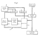
- Fig. 1 is a block diagram of a ciphering device, which forms a part of the present invention.
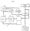
- Fig. 2 is block diagram of a deciphering device corresponding to the ciphering device of Fig. 1.
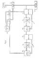
- Fig. 3 is a block diagram showing one embodiment of the ciphering device having double code units.
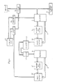
- Fig. 4 is a block diagram showing one embodiment of the ciphering device having a shift register and an EXOR gate between the code units.
- Fig. 5 is a block diagram showing one embodiment of the ciphering device having a shift register and a programmable memory between the two code units.
- Fig. 6 is a block diagram showing one embodiment of the ciphering device comprising a code handling system between the two code units.
- a ciphering device which is intended to be connected in a data link between a transmitting and a receiving unit, on the transmitting side.
- This ciphering device substantially comprises an input 1 for information in clear from the transmitting unit, an output 2 for ciphered information, a mixing unit 3 consisting of an EXOR gate, a code unit 4 for generating the code bits in the code bit sequence, and means 6, 7, 8 controlling certain selections in the device, as will be described in more detail hereinbelow.
- the code unit 4 which has an input connected to the output of the mixing unit 3, consists of a 16-bit shift register 9, a memory 5 which may be a byte-organized ROM or EPROM, and a multiplexer 10.
- the first thirteen bits of the shift register 9 are connected to the address inputs of the memory 5 and its last three bits are connected to the address inputs of the multiplexer 10.
- the outputs of the memory 5 are connected to the data inputs of the multiplexer 10.
- certain selections can be carried out in the ciphering device. The selections relate to whether an incoming data bit should be ciphered or not, and whether a ciphered bit should be loaded into the shift register 9 or not.
- a signal is supplied to one input of the means 7, which may consist of a logic AND gate, for determining whether the bit should be ciphered or not, and another signal is supplied to one input of the means 6, which may also consist of an AND gate, for determining whether the ciphered bit should be loaded into the register or not.
- the gate 7 receives on its other input a code bit from the multiplexer 10 and has its output connected to the mixing unit 3. The output of the gate 6 is connected to an enabling input of the register 9.
- the deciphering device shown in Fig. 2 is intended to be connected in the other end of the data link to which the ciphering device is connected, before the receiving unit.
- the deciphering device On its input 11, the deciphering device receives ciphered data from the ciphering device and, on its output 12, supplies deciphered data to the receiving unit.
- the deciphering device is built up in the same manner as the ciphering device, with the exception that the shift register 19 is connected to the input 11. Otherwise, the two devices consist of the same components and contain the same information (in the memories and the control units), and the deciphering device will therefore not be described in more detail here.
- the shift register 9 is loaded with ciphered bits from the output of the mixing unit 3.
- a memory cell in the memory 5 is addressed with the first thirteen bits in the register.
- the content of the memory cell is supplied to the data inputs of the multiplexer 10 which by means of the last three bits in the register 9 selects which of the eight bits in the addressed memory word should constitute a code bit.
- the control unit 8 supplies the gate 7 with a signal which indicates whether the code bit on the output of the multiplexer 10 should be supplied to the input of the mixing unit 3 and mixed with the bit concerned or whether this bit should pass through the mixing unit without being ciphered.
- control unit 8 emits to the gate 6 a signal which indicates whether the bit concerned should be loaded into the register 9 or not, after it has passed through the mixing unit 3. If the bit is loaded into the register, the address to the memory 5 and to the multiplexer 10 is changed, and a new code bit is obtained. In some cases, it may be convenient not to load bits from the mixing unit 3 into the register 9, for instance in the case of start and stop bits which when passing through unciphered always look the same. Naturally, this option also enhances the security of the system.
- the deciphering device operates in the same way. Since it is the same program that is in the control unit 18, the same bits will be loaded into the register 19, the same memory cells will be addressed in the memory 15 whose content must of course be the same as in the memory 5 of the ciphering device, the same code bits will be generated and the same bits will pass unciphered through the mixing unit 13. Thus, the ciphered bits will be mixed with the same code bits as they were mixed with in the ciphering device, and since the mixing unit consists of an EXOR gate, the original message will be recovered in clear on its output.
- the ciphering system is of such a simple design, it is completely protected also from those who know exactly how it operates.
- the result of the ciphering operation depends on the message ciphered, the content in the memory 5 and the program in the control unit 8. In order to decipher messages, it is thus necessary to have access to the content in the memory and the program in the control unit. If there is even the faintest suspicion that the content in the memory and/or the control unit is known, the memory and/or the program in the control unit may very easily be exchanged.
- the control unit may also store several programs which are alternatingly connected by means of a push-button set associated with the control unit.
- the components shown in Fig. 1 appear with the same reference numerals. These units operate in the same manner as in the device shown in Fig. 1 and, therefore, will not be described here.
- the device comprises a second code unit 4' the input of which is connected to the output of the first code unit 4 and which is designed in the same way as this, namely with a 16-bit shift register 9', a memory 5', which may be a byte-organized ROM or EPROM, and a multiplexer 10'.
- the code bits generated by the code unit 4 are supplied to the shift register 9', the first thirteen bits of which are used for addressing the memory 5' and the last three bits of which serve as input signal to the multiplexer 10' for selecting which bit in the word addressed in the memory 5' should constitute a code bit.
- the addresses to the memory unit 9 in the first code unit and the code from the memory 5' in the second code unit are related in no readable way to each other and, hence, it is not possible by tapping the input signals to and the output signals from the system, to map the content in the memories 5 and 5'.
- the deciphering device corresponding to this ciphering device is designed in a corresponding way and will therefore not be described here.
- the device of Fig. 3 is supplemented with a shift register 40 and an EXOR gate 41.
- the shift register 40 receives on its input the code bits generated by the code unit 4.
- the first and the last bit in the shift register 40 are used as input signals to the EXOR gate 41 whose output is connected to the shift register 9' in the second code unit 4'.
- the number of addresses which would have to be mapped to create a replacement memory for the memories 5 and 5' is considerably increased. If the length of the shift register 40 and of the shift registers 9 and 9' is 16 bits, the required number of addresses will be 2.81 x 10¹⁴.
- the corresponding deciphering device (not shown) has a shift register and an EXOR gate which are connected in the same manner.
- Fig. 5 there is shown a variant of the device illustrated in Fig. 4, in which the EXOR gate 41 has been replaced by a read-write memory 42 which is addressed with the content in the shift register 40 and the output of which is connected to the shift register 9' in the second code unit 4'.
- the content in the memory 42 can be exchanged by programming a new code from a keyboard 43.
- the purpose of the memory 42 is to prevent the transmitted, ciphered information from being deciphered afterwards if anyone having tapped the transmitted information later appropriates a deciphering device. In order to decipher a message, it is thus necessary to have access to the code being in the memory 42 during the ciphering operation, and if this code is changed at regular intervals, subsequent deciphering will be impossible.
- the deciphering device (not shown) is designed correspondingly.
- Fig. 6 there is shown a variant of the ciphering device of Fig. 5, which overcomes the practical problems linked with the handling and transmission to the deciphering device of the codes which are supplied to the memory 42, and with the work effort required for thus supplying the codes at regular intervals.
- the variant of the ciphering device illustrated in Fig. 6 comprises, in addition to the shift register 40 and the memory 42, a computer 43 having an input which by a line 51 is connected to the output of the mixing unit 3, address outputs which by an address bus 44 are connected to the memory 42, an in/output which by a data line 45 is connected to the memory 42, and a control signal output for transmitting a read-write signal on a line 46 to the memory 42.
- the device further comprises a buffer 47 which is connected to the shift register 40 and in which the content in the shift register is temporarily stored and which has tristate outputs connectible to the address bus 44.
- the device comprises a clock 48 which is programmable from the computer 43 which may be a one-chip computer having a nonvolatile and a volatile memory.
- the memory of the computer contains an algorithm which is stored in software and by means of which the computer creates a new code for the memory 42. The code is created during different time periods, and the length of a current time period is determined by the code created during the preceding time period, the clock 48 being used for establishing when a time period is terminated.
- the code generated during a time period is finally created, it is temporarily stored in a buffer, awaiting the transmission to the memory 42.
- the computer 43 establishes suitable points of time for the transmission by analyzing the signals on the output from the mixing unit 3. When a predetermined event occurs, for example no signals present on the output, the code temporarily stored in the buffer is transmitted to the memory.
- the computer then disconnects the outputs of the buffer 47 from the address bus by means of a control signal on a line 50, emits a write signal on the line 46 and addresses the memory via the address bus 44 so that the generated code can be transmitted to the memory 42 by the data line 45.
- the deciphering device (not shown) corresponding to this embodiment of the ciphering device is designed in a corresponding way with shift register, buffer, computer, memory etc.
- the computer in the deciphering device generates a new code to its memory by means of the same algorithm as used by the computer 43 of the ciphering device.
- the computer of the deciphering device further relies on the same criteria as the computer 43 for deciding when the transmission of a new code to the memory should take place. In this manner, the content in the two memories will always be the same.
- the clock 48 is used for synchronizing purposes. Synchronization is performed in that certain predetermined events, e.g. certain bit patterns or interruptions in the information transmission, are used as time references for the clocks in both devices. When such a predetermined event occurs, the clock is set to a known state.
- certain predetermined events e.g. certain bit patterns or interruptions in the information transmission
Landscapes
- Engineering & Computer Science (AREA)
- Computer Security & Cryptography (AREA)
- Computer Networks & Wireless Communication (AREA)
- Signal Processing (AREA)
- Storage Device Security (AREA)
- Soil Working Implements (AREA)
- Motorcycle And Bicycle Frame (AREA)
- Jib Cranes (AREA)
- Reverberation, Karaoke And Other Acoustics (AREA)
- Radar Systems Or Details Thereof (AREA)
- Input Circuits Of Receivers And Coupling Of Receivers And Audio Equipment (AREA)
- Lock And Its Accessories (AREA)
- Control Of Vending Devices And Auxiliary Devices For Vending Devices (AREA)
- Coin-Freed Apparatuses For Hiring Articles (AREA)
Priority Applications (1)
| Application Number | Priority Date | Filing Date | Title |
|---|---|---|---|
| AT86903695T ATE83106T1 (de) | 1986-06-09 | 1986-06-09 | Einrichtung zur verschluesselung und zur entschluesselung. |
Applications Claiming Priority (1)
| Application Number | Priority Date | Filing Date | Title |
|---|---|---|---|
| PCT/SE1986/000275 WO1987007796A1 (en) | 1984-12-10 | 1986-06-09 | Ciphering and deciphering device |
Publications (2)
| Publication Number | Publication Date |
|---|---|
| EP0309447A1 EP0309447A1 (en) | 1989-04-05 |
| EP0309447B1 true EP0309447B1 (en) | 1992-12-02 |
Family
ID=20363182
Family Applications (1)
| Application Number | Title | Priority Date | Filing Date |
|---|---|---|---|
| EP86903695A Expired - Lifetime EP0309447B1 (en) | 1986-06-09 | 1986-06-09 | Ciphering and deciphering device |
Country Status (8)
| Country | Link |
|---|---|
| US (1) | US4972481A (da) |
| EP (1) | EP0309447B1 (da) |
| JP (1) | JPH01503028A (da) |
| AT (1) | ATE83106T1 (da) |
| DE (1) | DE3687235T2 (da) |
| DK (1) | DK60488D0 (da) |
| FI (1) | FI885698A7 (da) |
| NO (1) | NO880545D0 (da) |
Families Citing this family (13)
| Publication number | Priority date | Publication date | Assignee | Title |
|---|---|---|---|---|
| JPH04346127A (ja) | 1991-05-23 | 1992-12-02 | Sony Corp | 電子装置 |
| NL9102157A (nl) * | 1991-12-20 | 1993-07-16 | Nederland Ptt | Systeem voor het met een eerste codeerapparaat coderen van aangeboden data en voor het met een tweede codeerapparaat decoderen van gecodeerde data, en codeerapparaat voor toepassing in het systeem. |
| US5623665A (en) * | 1992-01-13 | 1997-04-22 | Sony Corporation | Electronic apparatus for patching a read-only memory |
| JP3230262B2 (ja) * | 1992-01-24 | 2001-11-19 | ソニー株式会社 | 電子装置及びその固定情報修正方法 |
| JP3284614B2 (ja) * | 1992-09-19 | 2002-05-20 | ソニー株式会社 | 電子装置 |
| JP3810805B2 (ja) * | 1992-09-19 | 2006-08-16 | ソニー株式会社 | 情報修正システム |
| NL9400428A (nl) * | 1994-03-18 | 1995-11-01 | Nederland Ptt | Inrichting voor het cryptografisch bewerken van datapakketten, alsmede werkwijze voor het genereren van cryptografische bewerkingsdata. |
| US7174014B2 (en) * | 2000-05-05 | 2007-02-06 | Teleputers, Llc | Method and system for performing permutations with bit permutation instructions |
| EP1230589A4 (en) * | 2000-05-05 | 2008-03-19 | Ruby B Lee | METHOD AND SYSTEM FOR PERFORMING PERMUTATIONS USING MODIFIED OMEGA AND EXCHANGE BASED PERMUTATION INSTRUCTIONS |
| US6922472B2 (en) | 2000-05-05 | 2005-07-26 | Teleputers, Llc | Method and system for performing permutations using permutation instructions based on butterfly networks |
| CN100428666C (zh) * | 2002-12-16 | 2008-10-22 | 中国电子科技集团公司第三十研究所 | 一种密码芯片密钥快速更换方法 |
| JP4492248B2 (ja) * | 2004-08-04 | 2010-06-30 | 富士ゼロックス株式会社 | ネットワークシステム、内部サーバ、端末装置、プログラム、およびパケット中継方法 |
| CN100546239C (zh) * | 2006-01-24 | 2009-09-30 | 马恒利 | 应用密文图技术对数据进行加密的方法 |
Family Cites Families (8)
| Publication number | Priority date | Publication date | Assignee | Title |
|---|---|---|---|---|
| US4404426A (en) * | 1962-05-23 | 1983-09-13 | American Standard Inc. | Cryptographic telegraphy programming system |
| US4176247A (en) * | 1973-10-10 | 1979-11-27 | Sperry Rand Corporation | Signal scrambler-unscrambler for binary coded transmission system |
| SE380696B (sv) * | 1974-03-20 | 1975-11-10 | Philips Svenska Ab | Sett att alstra en pseudoslumpbitfoljd och anordning for utforande av settet. |
| US4133974A (en) * | 1976-11-05 | 1979-01-09 | Datotek, Inc. | System for locally enciphering prime data |
| FR2467515A1 (fr) * | 1979-10-10 | 1981-04-17 | Telediffusion Fse | Systeme de chiffrement et de dechiffrement d'un signal numerique |
| US4596898A (en) * | 1984-03-14 | 1986-06-24 | Computer Security Systems, Inc. | Method and apparatus for protecting stored and transmitted data from compromise or interception |
| US4742544A (en) * | 1984-07-09 | 1988-05-03 | Kupnicki Richard A | Television transmission network with scrambling and descrambling |
| US4817148A (en) * | 1987-07-06 | 1989-03-28 | Wegener Communications, Inc. | Signal scrambling transmission system |
-
1986
- 1986-06-09 JP JP61503445A patent/JPH01503028A/ja active Pending
- 1986-06-09 DE DE8686903695T patent/DE3687235T2/de not_active Expired - Fee Related
- 1986-06-09 US US07/285,970 patent/US4972481A/en not_active Expired - Fee Related
- 1986-06-09 EP EP86903695A patent/EP0309447B1/en not_active Expired - Lifetime
- 1986-06-09 AT AT86903695T patent/ATE83106T1/de not_active IP Right Cessation
-
1988
- 1988-02-05 DK DK060488A patent/DK60488D0/da not_active Application Discontinuation
- 1988-02-08 NO NO1988880545A patent/NO880545D0/no unknown
- 1988-12-08 FI FI885698A patent/FI885698A7/fi not_active Application Discontinuation
Also Published As
| Publication number | Publication date |
|---|---|
| EP0309447A1 (en) | 1989-04-05 |
| FI885698A0 (fi) | 1988-12-08 |
| DK60488A (da) | 1988-02-05 |
| DE3687235T2 (de) | 1993-08-12 |
| FI885698A7 (fi) | 1988-12-08 |
| DK60488D0 (da) | 1988-02-05 |
| US4972481A (en) | 1990-11-20 |
| NO880545L (no) | 1988-02-08 |
| JPH01503028A (ja) | 1989-10-12 |
| NO880545D0 (no) | 1988-02-08 |
| DE3687235D1 (de) | 1993-01-14 |
| ATE83106T1 (de) | 1992-12-15 |
Similar Documents
| Publication | Publication Date | Title |
|---|---|---|
| US4322576A (en) | Message format for secure communication over data links | |
| US5301247A (en) | Method for ensuring secure communications | |
| US4386234A (en) | Cryptographic communication and file security using terminals | |
| US4206315A (en) | Digital signature system and apparatus | |
| EP0309447B1 (en) | Ciphering and deciphering device | |
| EP0002389B1 (en) | Multiple domain data communication | |
| KR100234447B1 (ko) | 안전한 통신링크의 확정방법 및 그장치 | |
| US5222136A (en) | Encrypted communication system | |
| US4809327A (en) | Encrtption of messages employing unique control words and randomly chosen encryption keys | |
| KR950010705B1 (ko) | 암호화/해독화 장치 및 그 통신 네트워크 | |
| CN1016555B (zh) | 数据加密密钥故障监视器 | |
| NO143601B (no) | Fremgangsmaate ved innstilling av kodetekstgeneratorer i chifreringsinnretninger | |
| US4133974A (en) | System for locally enciphering prime data | |
| WO1996002992A1 (en) | Signal transmitting method and communication system | |
| US4760600A (en) | Cipher system | |
| US4805216A (en) | Method and apparatus for continuously acknowledged link encrypting | |
| GB1379740A (en) | Method and apparatus for encoded messages transmission | |
| EP0651532A2 (en) | Method for sequential encryption/decryption of externally stored computer object code | |
| US4555591A (en) | Integrated circuit devices for secure data encryption | |
| WO1987007796A1 (en) | Ciphering and deciphering device | |
| AU601370B2 (en) | Ciphering and deciphering device | |
| GB2124808A (en) | Security system | |
| EP0592595A1 (en) | Ciphering device | |
| EP0619659A2 (en) | A shrinking generator for cryptosystems | |
| NO144591B (no) | Koblingsanordning til styring av semidupleks-anlegg til overfoering av data |
Legal Events
| Date | Code | Title | Description |
|---|---|---|---|
| PUAI | Public reference made under article 153(3) epc to a published international application that has entered the european phase |
Free format text: ORIGINAL CODE: 0009012 |
|
| 17P | Request for examination filed |
Effective date: 19881202 |
|
| AK | Designated contracting states |
Kind code of ref document: A1 Designated state(s): AT BE CH DE FR GB IT LI LU NL SE |
|
| 17Q | First examination report despatched |
Effective date: 19901004 |
|
| RAP1 | Party data changed (applicant data changed or rights of an application transferred) |
Owner name: SECURICRYPTO AB |
|
| GRAA | (expected) grant |
Free format text: ORIGINAL CODE: 0009210 |
|
| AK | Designated contracting states |
Kind code of ref document: B1 Designated state(s): AT BE CH DE FR GB IT LI LU NL SE |
|
| PG25 | Lapsed in a contracting state [announced via postgrant information from national office to epo] |
Ref country code: AT Effective date: 19921202 |
|
| REF | Corresponds to: |
Ref document number: 83106 Country of ref document: AT Date of ref document: 19921215 Kind code of ref document: T |
|
| REF | Corresponds to: |
Ref document number: 3687235 Country of ref document: DE Date of ref document: 19930114 |
|
| ITF | It: translation for a ep patent filed | ||
| ET | Fr: translation filed | ||
| PG25 | Lapsed in a contracting state [announced via postgrant information from national office to epo] |
Ref country code: LU Free format text: LAPSE BECAUSE OF NON-PAYMENT OF DUE FEES Effective date: 19930630 |
|
| PGFP | Annual fee paid to national office [announced via postgrant information from national office to epo] |
Ref country code: NL Payment date: 19930630 Year of fee payment: 8 |
|
| PGFP | Annual fee paid to national office [announced via postgrant information from national office to epo] |
Ref country code: SE Payment date: 19930902 Year of fee payment: 8 |
|
| PGFP | Annual fee paid to national office [announced via postgrant information from national office to epo] |
Ref country code: GB Payment date: 19930908 Year of fee payment: 8 Ref country code: DE Payment date: 19930908 Year of fee payment: 8 |
|
| PGFP | Annual fee paid to national office [announced via postgrant information from national office to epo] |
Ref country code: CH Payment date: 19930924 Year of fee payment: 8 |
|
| PLBE | No opposition filed within time limit |
Free format text: ORIGINAL CODE: 0009261 |
|
| STAA | Information on the status of an ep patent application or granted ep patent |
Free format text: STATUS: NO OPPOSITION FILED WITHIN TIME LIMIT |
|
| PGFP | Annual fee paid to national office [announced via postgrant information from national office to epo] |
Ref country code: BE Payment date: 19931019 Year of fee payment: 8 |
|
| 26N | No opposition filed | ||
| PG25 | Lapsed in a contracting state [announced via postgrant information from national office to epo] |
Ref country code: FR Effective date: 19940228 |
|
| REG | Reference to a national code |
Ref country code: FR Ref legal event code: ST |
|
| PG25 | Lapsed in a contracting state [announced via postgrant information from national office to epo] |
Ref country code: GB Effective date: 19940609 |
|
| PG25 | Lapsed in a contracting state [announced via postgrant information from national office to epo] |
Ref country code: SE Effective date: 19940610 |
|
| PG25 | Lapsed in a contracting state [announced via postgrant information from national office to epo] |
Ref country code: LI Effective date: 19940630 Ref country code: CH Effective date: 19940630 Ref country code: BE Effective date: 19940630 |
|
| BERE | Be: lapsed |
Owner name: SECURICRYPTO A.B. Effective date: 19940630 |
|
| PG25 | Lapsed in a contracting state [announced via postgrant information from national office to epo] |
Ref country code: NL Effective date: 19950101 |
|
| EUG | Se: european patent has lapsed |
Ref document number: 86903695.4 Effective date: 19950110 |
|
| GBPC | Gb: european patent ceased through non-payment of renewal fee |
Effective date: 19940609 |
|
| NLV4 | Nl: lapsed or anulled due to non-payment of the annual fee | ||
| REG | Reference to a national code |
Ref country code: CH Ref legal event code: PL |
|
| PG25 | Lapsed in a contracting state [announced via postgrant information from national office to epo] |
Ref country code: DE Effective date: 19950301 |
|
| EUG | Se: european patent has lapsed |
Ref document number: 86903695.4 |
|
| PG25 | Lapsed in a contracting state [announced via postgrant information from national office to epo] |
Ref country code: IT Free format text: LAPSE BECAUSE OF NON-PAYMENT OF DUE FEES Effective date: 20050609 |