EP0307325B1 - Steuerungskreis für eine Zündung - Google Patents
Steuerungskreis für eine Zündung Download PDFInfo
- Publication number
- EP0307325B1 EP0307325B1 EP88420284A EP88420284A EP0307325B1 EP 0307325 B1 EP0307325 B1 EP 0307325B1 EP 88420284 A EP88420284 A EP 88420284A EP 88420284 A EP88420284 A EP 88420284A EP 0307325 B1 EP0307325 B1 EP 0307325B1
- Authority
- EP
- European Patent Office
- Prior art keywords
- amplifier
- comparator
- current
- transistor
- resistor
- Prior art date
- Legal status (The legal status is an assumption and is not a legal conclusion. Google has not performed a legal analysis and makes no representation as to the accuracy of the status listed.)
- Expired - Lifetime
Links
Images

Classifications
-
- F—MECHANICAL ENGINEERING; LIGHTING; HEATING; WEAPONS; BLASTING
- F02—COMBUSTION ENGINES; HOT-GAS OR COMBUSTION-PRODUCT ENGINE PLANTS
- F02P—IGNITION, OTHER THAN COMPRESSION IGNITION, FOR INTERNAL-COMBUSTION ENGINES; TESTING OF IGNITION TIMING IN COMPRESSION-IGNITION ENGINES
- F02P3/00—Other installations
- F02P3/02—Other installations having inductive energy storage, e.g. arrangements of induction coils
- F02P3/04—Layout of circuits
- F02P3/05—Layout of circuits for control of the magnitude of the current in the ignition coil
- F02P3/051—Opening or closing the primary coil circuit with semiconductor devices
Definitions
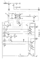
- the present invention relates to an ignition control circuit and in particular a so-called electronic control circuit for motor vehicles in which the spark of a spark plug is obtained at the secondary of a voltage-raising coil at the moment when the abrupt interruption of the current passing through the primary of this coil.
- FIG. 1 represents an example of such a conventional electronic ignition system, described for example in US-A-3 838 672, comprising an energy storage battery 1 (the battery of the automobile) and a lifting coil 2, the secondary of which is connected to a spark gap (3) and the primary of which is in series with an electronic switch 4, such as an assembly of Darlington transistors, allowing the current to pass or interrupt the current in the coil.
- a control member 5 makes it possible to control, as a function of information received from the motor 6, the closing then the opening of the switch 4, this control member acting on the base of the main switch which, in the example shown, is bipolar.
- switch 4 when the switch 4 is closed, current begins to flow in the primary of the coil and gradually increase.
- switch 4 opens, a spark occurs in the spark plugs 3.
- This detection circuit 7 in series with the power switch 4.
- This detection circuit comprises a resistor R1 of low value in parallel with a divider circuit comprising resistors R2 and R3, the voltage detected at the common point between the resistors R2 and R3 being proportional to the current passing through the resistor R1.
- This detected voltage V D is compared to a reference voltage 8 in a controlled comparator amplifier 9 whose output supplies a basic current to the power switch 4.
- the amplifier 9, produced in an integrated circuit is a high gain amplifier, for example with three stages. Current technologies mean that this gain can vary for each stage by a factor of 3, for example between 100 and 300. Similarly, the gain of the power switch 4, which is for example a Darlington assembly with several stages, can vary considerably , for example by a factor of 30. Under these conditions, it is very difficult in practice to ensure a predetermined value for the loop gain of the servo and consequently to ensure the stability of the servo in current.
- An object of the present invention is to provide an ignition control circuit whose control in the current limitation phase is stable thanks to a predictable loop gain.
- Another object of the present invention is to provide that this control circuit which is constituted in practice by a specialized integrated circuit can be used in connection with different bipolar Darlington transistors or.
- an object of the invention is to make the contribution to the loop gain of the amplifier contained in the control member reproducible when the latter is produced in the form of an integrated circuit.
- Another object of the present invention is to make this contribution externally adjustable so as to be able to compensate for the differences in gain provided by the different types of power members.
- the present invention provides a control circuit comprising a bipolar power switch in series with the primary of an ignition coil and a detection resistor; a voltage divider in parallel on the detection resistor providing a detected voltage proportional to the current in the resistance; a controlled comparator amplifier, the first input of which receives the detected voltage and the second input of which receives a reference voltage, the output of which is connected to the base of the power switch and the control input of which can receive a signal inhibition order, this amplifier-comparator acting to limit the base current when the detected voltage approaches the reference voltage; a series resistor between the output of the comparator amplifier and the base of the power switch; and a differential amplifier whose inputs are connected to the terminals of the series resistor and whose output is connected to the first input of the comparator amplifier.
- this circuit further comprises means for inhibiting the action of the differential amplifier when the detected voltage is less than a selected threshold at most equal to the reference voltage.
- the differential amplifier comprises multi-collector transistors whose emitters are connected to the terminals of the series resistor, whose first collectors are interconnected and whose second collectors are connected to active loads consisting of transistors connected in current mirror .
- the resistors of the voltage divider are adjustable so that their ratio is adjusted to obtain a limitation of the current in the power switch to a predetermined value and that the absolute value of the resistance in series with the input of the amplifier-comparator is chosen to determine the gain of the servo circuit.
- This amplifier 9 acts on the control terminal of the power switch 4 via a resistor R10 in series.
- This resistor R10 constitutes a means of measuring the input current into the control terminal, commonly the base, of the bipolar power switch 4.
- a differential amplifier 11 of transconductance y D (ratio between the variation of output current and the variation of input voltage) has its inputs connected to the terminals of the resistor R10.
- the output of this differential amplifier 11 is connected to the first input of the amplifier-comparator 9 in a direction such that the loop formed by this amplifier-comparator, the resistor R10 and the differential amplifier 11 performs a feedback.
- the adjustment of the potentiometer R2, R3 has a double function: by adjusting R2, the gain of the control loop is fixed, by adjusting the ratio R2 / R3, the desired level of current limitation is fixed in the power switch.
- a drawback of the circuit according to the present invention as described above could be that, from the initial phase of closing the power switch 4, the differential amplifier 11 begins to act to reduce the base current in this power switch and therefore to slow the rate of current increase in the coil primary.
- the output of comparator 12 inhibits the operation of the differential amplifier 11 as long as the detected voltage, ie ie the current in the resistor R1, has not reached a certain threshold. It is only from this threshold that the feedback begins to act.
- FIG. 3 represents a detailed embodiment of certain elements of the circuit shown very schematically in FIG. 2.
- the amplifier-comparator 9 comprises an amplification chain made up of PNP T57 and NPN T59 and T62 transistors. At its input, there are two NPN transistors T51 and T55 mounted as a comparator, the emitter of transistor T51 being connected to an input terminal E9 which receives the signal V D coming from the connection point of the resistors R2 and R3 mentioned above .
- the emitter of transistor T55 is connected to a resistor R8 which defines, in relation to a current source I8, the reference voltage represented by the voltage source 8 in FIGS. 1 and 2.
- the input comparator includes the following connections.
- the transistor T51 is connected by its collector to a current source I51 whose other terminal is connected to the supply voltage VCC.
- the emitter of transistor T51 is connected to terminal E9 as indicated above, the base of transistor T51 is connected to its collector and to the base of transistor T55.
- the collector of transistor T55 is connected to the supply voltage VCC by a current source I8 and its emitter is connected to ground via a resistor R8.
- the signal at the output terminal 23 of the comparator is connected to the input transistor T57 of the amplifier circuit comprising the transistors T57, T59 and T62.
- the amplification part includes the following connections.
- the PNP transistor T57 whose base is connected to the output terminal 23 of the comparator has its transmitter connected to a current source I57 itself connected to the supply voltage VCC.
- the collector of transistor T57 is connected to ground by a transistor T45 maintained in the on state.
- the emitter and the collector of transistor T57 are connected to ground via NPN transistors T56 and T60, the role of which will be explained below.
- the emitter of transistor T57 is also connected to the base of the second NPN-type transistor T59 whose collector is connected to terminal VCC by a current limiting resistor R59 and whose emitter is connected to ground via a transistor T61 whose role will be explained below.
- the emitter of transistor T59 is also connected to the base of transistor T62 whose collector is connected to terminal VCC by a current limiting resistor R62 and whose emitter is connected to ground via a resistor R61 and to the output terminal S9 of circuit 9.
- the three transistors T56, T60 and T61 contained in a block 30 constitute the inhibition control circuit of the amplifier 9.
- This circuit receives a signal from a control input terminal EC9 connected to a processing circuit signal receiving information from the motor 6. It will be seen that the circuit 30 also serves to disable the differential amplifier 11.
- the differential amplifier 11 has its input terminals connected to the terminals of the resistor R10 and its output terminal A connected to the terminal A indicated in block 9 at the emitter of transistor T51, that is to say tell at terminal E9 where the detected voltage V D is applied.
- This differential amplifier 11 includes two input resistors R11 and R12 connected to the emitters of PNP transistors with two collectors T63 and T70 mounted in differential, that is to say connected by their bases, and has a constant gain thanks to an interconnection of the second collectors.
- the first collectors are connected to ground by a load made up of two NPN transistors T76 and T77 connected in current mirror.
- the collectors of transistors T76 and T77 are respectively connected to the collectors of transistors T63 and T70, their emitters being grounded, their bases being interconnected and the collector and the base of transistor T77 being connected.
- the signal on the collector of transistor T76 which is the amplified image of the current in the resistor R10, is supplied to the output terminal A, via a transistor T78 mounted as a diode, to provide a feedback. .
- the control of the transistor T79 is ensured by a circuit comprising, between the voltage VCC and the ground, a resistor R16, a transistor T43 and a resistor R20.
- the base of transistor T43 is connected to the collector of transistor T45 and the emitter of transistor T43 is connected to the base of transistor T79.
- the output current of the differential amplifier 11 is available on the collectors of the transistors T63 and T76.
- the role of transistor T78, connected as a diode, is to allow transistor T76 to operate with a sufficient collector voltage; indeed the terminal E9 always remains at a potential close to that of the ground.
Landscapes
- Engineering & Computer Science (AREA)
- Chemical & Material Sciences (AREA)
- Combustion & Propulsion (AREA)
- Mechanical Engineering (AREA)
- General Engineering & Computer Science (AREA)
- Ignition Installations For Internal Combustion Engines (AREA)
- Amplifiers (AREA)
- Electrical Control Of Ignition Timing (AREA)
Claims (5)
- Steuerschaltung für eine Zündung, mit:- einem bipolaren Leistungsschalter (40), der in Reihe mit der Primärseite einer Zündspule (2) und einem Detektor-Widerstand (R1) geschaltet ist,- einem Spannungsteiler (R2, R3), der zum Detektor-Widerstand parallel liegt und eine erfaßte, zum Strom in diesem Detektor-Widerstand (R1) proportionale Spannung liefert,- einem gesteuerten Verstärker-Vergleicher (9), dessen erster Eingang (E9) die erfaßte Spannung (VD) empfängt und dessen zweiter Eingang eine Bezugsspannung (8) empfängt, dessen Ausgang mit der Basis des Leistungsschalters (4) verbunden ist und dessen Steuereingang (EC9) ein Sperr-Befehlssignal empfangen kann, wobei der Verstärker-Vergleicher den Basisstrom begrenzt, wenn die erfaßte Spannung sich der Bezugsspannung annähert,
gekennzeichnet durch:
- einen Reihenwiderstand (R10) zwischen dem Ausgang des Verstärker-Vergleichers (9) und der Basis des Leistungsschalters (4) und- einen Differentialverstärker (11), dessen Eingänge mit den Anschlüssen des Reihenwiderstandes verbunden sind und dessen Ausgang (A) mit dem ersten Eingang (E9) des Verstärker-Vergleichers (9) verbunden ist. - Steuerschaltung für eine Zündung nach Anspruch 1, gekennzeichnet durch eine Vorrichtung (12; B, T79) zum Sperren der Tätigkeit des Differentialverstärkers (11), wenn die erfaßte Spannung niedriger als ein gegebener Schwellwert ist, der maximal gleich der Bezugsspannung gewählt ist.
- Steuerschaltung für eine Zündung nach Anspruch 1 oder 2, dadurch gekennzeichnet, daß der Differentialverstärker (11) Transistoren mit zwei Kollektoren (T63, T70) aufweist, deren Emitter mit den Anschlüssen des Reihenwiderstandes (R10) verbunden sind, wobei die ersten Kollektoren miteinander verbunden sind und die zweiten Kollektoren mit aktiven Lasten (T77,T78) verbunden sind, welche von in Strom-Spiegelschaltung verbundenen Transistoren (T77, T78) gebildet sind.
- Steuerschaltung für eine Zündung nach einem der Ansprüche 1 bis 3, dadurch gekennzeichnet, daß der Spannungsteiler ein ohmscher Spannungsteiler ist, bei dem die Widerstände (R2, R3) einstellbar sind, so daß ihr Verhältnis zum Steuern des Strom-Grenzwertes des Leistungsschalters (4) einstellbar ist, und daß der Absolutwert des Widerstandes (R2) dieses Teilers, der zwischen dem zweiten Eingang des Verstärker-Vergleichers (9) und dem bipolaren Leistungsschalter (4) angeschlossen ist, zum Festlegen der Verstärkung der diesen Verstärker-Vergleicher umfassenden Schleife gewählt wird.
- Steuerschaltung für eine Zündung nach Anspruch 1, gekennzeichnet durch eine Vorrichtung (30) zum plötzlichen Einschalten oder Unterbrechen der Tätigkeit des Verstärker-Vergleichers (9).
Applications Claiming Priority (2)
| Application Number | Priority Date | Filing Date | Title |
|---|---|---|---|
| FR8712103A FR2619859B1 (fr) | 1987-08-27 | 1987-08-27 | Circuit de commande d'allumage |
| FR8712103 | 1987-08-27 |
Publications (2)
| Publication Number | Publication Date |
|---|---|
| EP0307325A1 EP0307325A1 (de) | 1989-03-15 |
| EP0307325B1 true EP0307325B1 (de) | 1993-03-10 |
Family
ID=9354524
Family Applications (1)
| Application Number | Title | Priority Date | Filing Date |
|---|---|---|---|
| EP88420284A Expired - Lifetime EP0307325B1 (de) | 1987-08-27 | 1988-08-23 | Steuerungskreis für eine Zündung |
Country Status (7)
| Country | Link |
|---|---|
| US (1) | US4912373A (de) |
| EP (1) | EP0307325B1 (de) |
| JP (1) | JP2621946B2 (de) |
| KR (1) | KR890004068A (de) |
| DE (1) | DE3879051T2 (de) |
| ES (1) | ES2038781T3 (de) |
| FR (1) | FR2619859B1 (de) |
Families Citing this family (10)
| Publication number | Priority date | Publication date | Assignee | Title |
|---|---|---|---|---|
| DE3839039A1 (de) * | 1988-11-18 | 1990-05-23 | Bosch Gmbh Robert | Zuendendstufe einer transistor-zuendanlage |
| US5043633A (en) * | 1989-11-13 | 1991-08-27 | Ncr Corporation | Circuit and method for regulating the current flow in a distributorless ignition system coil |
| JP2568813Y2 (ja) * | 1992-02-19 | 1998-04-15 | 三菱電機株式会社 | 内燃機関用点火装置 |
| US5446385A (en) * | 1992-10-02 | 1995-08-29 | Robert Bosch Gmbh | Ignition system for internal combustion engines |
| EP0639894B1 (de) * | 1993-08-18 | 1997-02-12 | Co.Ri.M.Me. Consorzio Per La Ricerca Sulla Microelettronica Nel Mezzogiorno | Schaltung zur Begrenzung des Maximalstroms, den ein Leistungstransistor an eine Last liefert |
| JP3530714B2 (ja) * | 1997-05-26 | 2004-05-24 | 株式会社日立製作所 | 内燃機関用点火装置 |
| DE102004013561B4 (de) * | 2004-03-19 | 2007-02-22 | Audi Ag | Verfahren und Schaltvorrichtung zum Betreiben einer Zündspule eines Kraftfahrzeugs |
| DE102008000871B4 (de) * | 2008-03-28 | 2021-07-01 | Robert Bosch Gmbh | Schaltungsanordnung zum Schalten des Stromflusses durch eine Zündspule |
| JP5253012B2 (ja) * | 2008-06-24 | 2013-07-31 | ローム株式会社 | パワー半導体の駆動回路装置およびそれに用いる信号伝達回路装置 |
| SE542389C2 (en) | 2018-09-04 | 2020-04-21 | Sem Ab | An ignition system and method controlling spark ignited combustion engines |
Family Cites Families (4)
| Publication number | Priority date | Publication date | Assignee | Title |
|---|---|---|---|---|
| US3838672A (en) * | 1973-08-23 | 1974-10-01 | Gen Motors Corp | Internal combustion engine ignition system |
| JPS54158536A (en) * | 1978-06-02 | 1979-12-14 | Hitachi Ltd | Current control circuit for ignition device |
| DE2829828C2 (de) * | 1978-07-07 | 1986-09-25 | Robert Bosch Gmbh, 7000 Stuttgart | Für eine Brennkraftmaschine bestimmte Zündanlage |
| US4574221A (en) * | 1984-01-04 | 1986-03-04 | Motorola, Inc. | Ignition control integrated circuit having substrate injection preventing means |
-
1987
- 1987-08-27 FR FR8712103A patent/FR2619859B1/fr not_active Expired - Fee Related
-
1988
- 1988-08-11 US US07/231,061 patent/US4912373A/en not_active Expired - Lifetime
- 1988-08-16 KR KR1019880010415A patent/KR890004068A/ko not_active Withdrawn
- 1988-08-23 DE DE8888420284T patent/DE3879051T2/de not_active Expired - Fee Related
- 1988-08-23 EP EP88420284A patent/EP0307325B1/de not_active Expired - Lifetime
- 1988-08-23 ES ES198888420284T patent/ES2038781T3/es not_active Expired - Lifetime
- 1988-08-25 JP JP63209630A patent/JP2621946B2/ja not_active Expired - Lifetime
Also Published As
| Publication number | Publication date |
|---|---|
| KR890004068A (ko) | 1989-04-19 |
| US4912373A (en) | 1990-03-27 |
| DE3879051T2 (de) | 1993-09-16 |
| FR2619859B1 (fr) | 1990-01-12 |
| DE3879051D1 (de) | 1993-04-15 |
| FR2619859A1 (fr) | 1989-03-03 |
| JPS6473168A (en) | 1989-03-17 |
| ES2038781T3 (es) | 1993-08-01 |
| JP2621946B2 (ja) | 1997-06-18 |
| EP0307325A1 (de) | 1989-03-15 |
Similar Documents
| Publication | Publication Date | Title |
|---|---|---|
| EP1093044B1 (de) | Linearer Regler mit niedrigem seriellen Spannungsabfall | |
| EP0307325B1 (de) | Steuerungskreis für eine Zündung | |
| EP0408436B1 (de) | Detektionsschaltung für ein Drehstromgenerator-Überwachungssignal eines Reglers zum Laden der Batterie eines Kraftfahrzeuges und seine Verwendung | |
| FR2677793A1 (fr) | Circuit pour produire une tension d'alimentation interne. | |
| FR2536921A1 (fr) | Regulateur a faible tension de dechet | |
| EP0029767B1 (de) | Steuerungsverfahren einer Darlingtonschaltung und Darlingtonschaltung mit geringen Verlusten | |
| FR3102581A1 (fr) | Régulateur de tension | |
| EP1083471A1 (de) | Spannungsregler | |
| FR2632070A1 (fr) | Circuit de commande de l'alimentation d'une charge electrique, a dispositif de detection d'un court-circuit de la charge | |
| FR2493636A1 (fr) | Circuit comparateur mos | |
| FR2607278A1 (fr) | Circuit integrable de regulation de courant dans une charge inductive et son application a la commande de bobine d'allumage d'un moteur a combustion interne | |
| FR3102580A1 (fr) | Régulateur de tension | |
| FR2672705A1 (fr) | Circuit generateur d'une tension de reference variable en fonction de la temperature, notamment pour regulateur de la tension de charge d'une batterie par un alternateur. | |
| EP0338926A1 (de) | Vorrichtung zur Hochspannungsstromversorgung des Betriebsstromkreises eines Kraftfahrzeuges | |
| EP0561456B1 (de) | Schneller Schaltstromspiegel | |
| EP0798910B1 (de) | Überspannungsschutz für eine Fernsprechleitungsschnittstelle | |
| EP0910002B1 (de) | Verfahren zur Herstellung eines sehr genauen Stroms | |
| FR2524732A1 (fr) | Circuit de protection contre les surcharges | |
| EP0230176B1 (de) | Statisches Relais, sowie Anwendung dieses Relais bei einem bipolaren Inverter oder bei einer Schaltung mit beliebiger Stromrichtung | |
| EP0716508A1 (de) | Steuerschaltung für elektronischen Schalter und diese verwendender Schalter | |
| EP0216697B1 (de) | Steuervorrichtung für einen Ausgangskreis einer integrierten Schaltung | |
| EP1113352B1 (de) | Steuervorrichtung | |
| EP0529735B1 (de) | Zündeinrichtung für eine Brennkraftmaschine | |
| FR2654880A1 (fr) | Circuit integre de puissance "intelligent" du type mos, pour la commande de l'alimentation d'une charge electrique. | |
| EP0122820B1 (de) | Regler für einen Batterieladegenerator |
Legal Events
| Date | Code | Title | Description |
|---|---|---|---|
| PUAI | Public reference made under article 153(3) epc to a published international application that has entered the european phase |
Free format text: ORIGINAL CODE: 0009012 |
|
| AK | Designated contracting states |
Kind code of ref document: A1 Designated state(s): DE ES FR GB IT NL SE |
|
| 17P | Request for examination filed |
Effective date: 19890825 |
|
| 17Q | First examination report despatched |
Effective date: 19920513 |
|
| GRAA | (expected) grant |
Free format text: ORIGINAL CODE: 0009210 |
|
| AK | Designated contracting states |
Kind code of ref document: B1 Designated state(s): DE ES FR GB IT NL SE |
|
| PG25 | Lapsed in a contracting state [announced via postgrant information from national office to epo] |
Ref country code: SE Effective date: 19930310 Ref country code: NL Effective date: 19930310 |
|
| ITF | It: translation for a ep patent filed | ||
| REF | Corresponds to: |
Ref document number: 3879051 Country of ref document: DE Date of ref document: 19930415 |
|
| GBT | Gb: translation of ep patent filed (gb section 77(6)(a)/1977) |
Effective date: 19930423 |
|
| REG | Reference to a national code |
Ref country code: ES Ref legal event code: FG2A Ref document number: 2038781 Country of ref document: ES Kind code of ref document: T3 |
|
| NLV1 | Nl: lapsed or annulled due to failure to fulfill the requirements of art. 29p and 29m of the patents act | ||
| PLBE | No opposition filed within time limit |
Free format text: ORIGINAL CODE: 0009261 |
|
| STAA | Information on the status of an ep patent application or granted ep patent |
Free format text: STATUS: NO OPPOSITION FILED WITHIN TIME LIMIT |
|
| 26N | No opposition filed | ||
| REG | Reference to a national code |
Ref country code: FR Ref legal event code: D6 |
|
| PGFP | Annual fee paid to national office [announced via postgrant information from national office to epo] |
Ref country code: FR Payment date: 20000811 Year of fee payment: 13 |
|
| PGFP | Annual fee paid to national office [announced via postgrant information from national office to epo] |
Ref country code: DE Payment date: 20000814 Year of fee payment: 13 |
|
| PGFP | Annual fee paid to national office [announced via postgrant information from national office to epo] |
Ref country code: GB Payment date: 20000823 Year of fee payment: 13 |
|
| PGFP | Annual fee paid to national office [announced via postgrant information from national office to epo] |
Ref country code: ES Payment date: 20000830 Year of fee payment: 13 |
|
| PG25 | Lapsed in a contracting state [announced via postgrant information from national office to epo] |
Ref country code: GB Free format text: LAPSE BECAUSE OF NON-PAYMENT OF DUE FEES Effective date: 20010823 |
|
| PG25 | Lapsed in a contracting state [announced via postgrant information from national office to epo] |
Ref country code: ES Free format text: LAPSE BECAUSE OF NON-PAYMENT OF DUE FEES Effective date: 20010824 |
|
| GBPC | Gb: european patent ceased through non-payment of renewal fee |
Effective date: 20010823 |
|
| PG25 | Lapsed in a contracting state [announced via postgrant information from national office to epo] |
Ref country code: FR Free format text: LAPSE BECAUSE OF NON-PAYMENT OF DUE FEES Effective date: 20020430 |
|
| PG25 | Lapsed in a contracting state [announced via postgrant information from national office to epo] |
Ref country code: DE Free format text: LAPSE BECAUSE OF NON-PAYMENT OF DUE FEES Effective date: 20020501 |
|
| REG | Reference to a national code |
Ref country code: FR Ref legal event code: ST |
|
| REG | Reference to a national code |
Ref country code: ES Ref legal event code: FD2A Effective date: 20020911 |
|
| PG25 | Lapsed in a contracting state [announced via postgrant information from national office to epo] |
Ref country code: IT Free format text: LAPSE BECAUSE OF NON-PAYMENT OF DUE FEES;WARNING: LAPSES OF ITALIAN PATENTS WITH EFFECTIVE DATE BEFORE 2007 MAY HAVE OCCURRED AT ANY TIME BEFORE 2007. THE CORRECT EFFECTIVE DATE MAY BE DIFFERENT FROM THE ONE RECORDED. Effective date: 20050823 |