EP0307196A2 - Randgekoppelte magnetostatische Wellenstrukturen - Google Patents
Randgekoppelte magnetostatische Wellenstrukturen Download PDFInfo
- Publication number
- EP0307196A2 EP0307196A2 EP88308298A EP88308298A EP0307196A2 EP 0307196 A2 EP0307196 A2 EP 0307196A2 EP 88308298 A EP88308298 A EP 88308298A EP 88308298 A EP88308298 A EP 88308298A EP 0307196 A2 EP0307196 A2 EP 0307196A2
- Authority
- EP
- European Patent Office
- Prior art keywords
- block
- magnetostatic
- magnetostatic wave
- blocks
- ferrimagnetic material
- Prior art date
- Legal status (The legal status is an assumption and is not a legal conclusion. Google has not performed a legal analysis and makes no representation as to the accuracy of the status listed.)
- Withdrawn
Links
Images
Classifications
-
- H—ELECTRICITY
- H03—ELECTRONIC CIRCUITRY
- H03H—IMPEDANCE NETWORKS, e.g. RESONANT CIRCUITS; RESONATORS
- H03H2/00—Networks using elements or techniques not provided for in groups H03H3/00 - H03H21/00
- H03H2/001—Networks using elements or techniques not provided for in groups H03H3/00 - H03H21/00 comprising magnetostatic wave network elements
Definitions
- This invention relates in general to magnetostatic wave structures and relates more particularly to the coupling between such structures.
- Yttrium-Iron-Garnet (YIG) devices are widely used in combination with an applied magnetic field to accomplish wide band tuning in microwave circuits. These YIG devices are typically coupled by microstrip conductors. In the case of a YIG sphere, the microstrip conductor partially encircles the sphere in order to strongly couple to the magnetic field associated with the YIG sphere. Changes in the magnetic field surrounding the YIG sphere induces in this conductor a current which is carried by the conductor to an area within the magnetic field of another YIG sphere.
- Magnetostatic Wave (MSW) resonators have been produced that utilize shallow etched gratings or overlying metal gratings to selectively couple to particular wavelengths of the magnetostatic waves in the resonator, see, for example, the article by J.P. Casters, et al entitled A TUNABLE MAGNETOSTATIC VOLUME WAVE OSCILLATOR in the IEEEMTT-S International Microwave Symposium Digest (1983) .
- these structures have a very high loss and their performance is critically dependent on the etch depth and metal thickness, respectively, of the gratings. Therefore, it would be advantageous to have a low loss coupling mechanism between MSW devices.
- a magnetostatic wave structure characterised in that it comprises a first block of ferrimagnetic material of lengths L and width W having a first end means for launching a magnetostatic travelling wave (I) in said first block toward said first end, said wave (I) producing an associated electromagnetic field that extends past the first end of the first block, and a second block of ferrimagnetic material having a second end positioned end to end with the first end and located within a distance D, equal to the smaller of 4L and 4W, of the first end of the first block so that said electromagnetic field produced by the magnetostatic wave (I) interacts directly with the ferrimagnetic material in the second block thereby launching a magnetostatic wave (T) in said second block, said blocks having no magnetic shielding between said first and second ends, whereby signals in said first block are coupled into said second block.
- An advantage of the above arrangement is that a wave travelling in one block towards an end thereof produces an electromagnetic field that interacts directly with the ferrimagnetic material in another block with sufficient amplitude to launch a magnetostatic wave in the second block.
- the first and second blocks have fundamental resonant modes that have wavelengths much greater than the spacing between the first and second ends.
- the second block may have a third edge spaced from a third block with a fourth edge, the second and third blocks having fundamental resonance modes that have wavelengths much greater than the spacing between the third and fourth ends.
- the structure may comprise means for sensing magnetostatic waves in the pth block, for some integer p in the range 1 ⁇ p ⁇ N, and for generating an output signal in response to the magnetostatic waves sensed in the pth block.
- is greater than 1, whereby the spacing between said means for launching magnetostatic waves and said means for sensing magnetostatic waves is increased over the spacing that would result for
- 1, whereby any direct electromagnetic coupling between said means for launching and said means for sensing that is not transmitted by magnetostatic waves in said blocks is reduced.
- the blocks may have dimensions such that, for the kth block for k - 1,...,N, there exists a resonance peak at a frequency f k and the f k are spaced so that said means for launching and said means for sensing exhibit a transfer function that is substantially flat between f min and f max .
- a coupling mechanism for coupling together magnetostatic wave (MSW) devices that utilize thin films of a ferrimagnetic material such as yttrium-iron-garnet.
- MSW magnetostatic wave
- a pair of such film devices are coupled together by mounting the two thin films on a substrate such that the spacing between these two films is small enough that a magnetic wave propagating towards the edge of a first of these thin films launches a magnetic wave into the other thin film.
- the magnetic field produced by the YIG film extends beyond the sides as well as beyond the ends of the thin film.
- the signals in two YIG films can be coupled by closely spacing the two YIG films either end to end or side by side.
- these ends and sides of adjacent blocks will be parallel so that a wave that is parallel or perpendicular to an end of one block will also be parallel or perpendicular to an end of the adjacent block.
- these sides or ends of adjacent blocks will be intentionally aligned at an angle that couples a particular wave mode in one block to a different mode in the adjacent block.
- Different types of thin film devices can also be coupled.
- this coupling scheme can be used to couple a thin film YIG delay line to a thin film YIG resonator.
- two or more resonators of differing lengths can be coupled together in this manner to produce a wide band resonator.
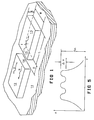
- Figure 1 is illustrated a coupling between two or more magnetostatic wave devices without use of interconnecting conductors.
- a dielectric material such as gadolinium gallium garnet, quartz or sapphire
- a pair of rectangular blocks 12 and 13 of a thin film of a ferromagnetic material, such a yttrium-iron-garnet (YIG) blocks 12 and 13 CaN be formed by cutting these blocks from a thin YIG film by use of a wafer saw and then mounting them on substrate 11 or they can be formed by growing by liquid phase epitaxy (LPE) a thin YIG film on the gadolinium gallium garnet and then patterning it by photolithographic techniques to produce blocks 12 and 13. This latter method is preferred because of the ease of manufacture, the accuracy of alignment of the blocks and the smoothness of the edges of the blocks.
- LPE liquid phase epitaxy
- a magnetostatic wave I travels toward an end 14 of block 12
- the magnetic field produced by this wave will interact with the magnetic dipoles in block 13 and will launch a wave T in that block.
- part of the incident wave I will be reflected into a reflected wave R in block 12 and part of the incident will launch a transmitted wave T in block 13.
- the thickness t of blocks 12 and 13 is of the order of 100 microns.
- the distance D will typically be on the order of or greater than 100 microns.
- An anisotropic etch process can be used to etch walls 14 and 15, but such an anisotropic etch process would take a much longer time than an isotropic chemical etch and therefore will generally not be the preferred method of forming blocks 12 and 13. However, in embodiments in which a spacing closer than 100 microns is required, an anisotropic etch process could be used.
- the lengths L of the YIG blocks are of the order of 800-1000 microns and the widths W of the YIG blocks are of the order of 2000-3000 microns so that the spacing between the blocks is typically much smaller than the wavelength of the fundamental resonant modes of the YIG blocks. As a result of this, there is a very strong coupling between the two blocks.
- the spacing between the blocks is selected to be of the order of or less than a few times the wavelength of the fundamental mode of each block and is preferably selected to be less than 1/16 of the wavelength of the fundamental mode to achieve strong coupling.
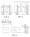
- Figure 2 is illustrated an embodiment in which a pair of one port resonators are coupled together in the manner illustrated in Figure 1.
- a first resonator (consisting of a block 22 of YIG film and a microstrip transducer 26) and a second resonator (consisting of a block 23 of YIG film and a microstrip transducer 27) are positioned with closely spaced edges 24 and 25.
- This combination functions as a two port resonator in which transducer 26 functions as the input and transducer 27 functions as the output port.
- transducer 26 not only generates magnetostatic waves in block 26, it also generates radio waves that can interact directly with transducer 27. Such direct action is a spurious coupling between these two transducers that does not exhibit the resonant behaviour produced by the magnetostatic waves in blocks 22 and 23. Because of the relatively close spacing of the first and second resonators, this direct coupling will be more significant than in previous coupling methods in which the first and second resonators will generally be spaced at a greater distance.
- the first resonator consists of a block 32 of YIG film and a microstrip transducer 36.
- the second resonator consists of a block 33 of YIG film and a microstrip transducer 37.
- An additional block 38 of YIG film is located between blocks 32 and 33 to couple the first resonator to the second resonator.
- a first end 39 of block 38 is positioned close to an end 34 of block 32 in order to couple the signal from block 32 into block 38.
- a second end 39′ of block 38 is positioned close to an end 35 of block 33 to couple the signal from block 38 into block 33.
- the spacing S′ between transducers 36 and 37 is much greater than the spacing between transducers 26 and 27 in Figure 2 so that the direct electromagnetic wave coupling, which drops off roughly as the inverse of the distance between the transducers, is significantly reduced in the embodiment of Figure 3 compared to the embodiment in Figure 2.
- FIG 4 a magnetostatic wave device in which a magnetostatic wave delay line (consisting of a block 42 of YIG film and a transducer 46) is coupled in a nonlinear arrangement to a magnetostatic wave resonator(consisting of a block 43 of YIG film and a microstrip transducer 47).
- the delay line includes an absorbing medium 49, such as a thin coating of metal particles, to absorb magnetostatic waves travelling toward an end 49′ of the magnetostatic wave delay line. Therefore, an input signal at transducer 46 launches a magnetostatic wave I in block 42 in the direction indicated by arrow 410.
- This magnetostatic wave I launches magnetostatic waves in YIG block 48 and these magnetostatic waves in turn induce magnetostatic waves in block 43.
- This embodiment illustrates that different types of magnetostatic wave devices can be coupled together by the coupling illustrated in Figure 1 and also illustrates that such couplings need not be in a strictly linear arrangement.
- FIG. 5 is shown a plot of the transfer function S21 between input transducer 36 and output transducer 37 as a function of the frequency f of a sinusoidal signal V applied to input transducer 36.
- ⁇ f k is the halfwidth of the kth resonant peak.
- the adjacent edges of adjacent blocks are generally aligned to be substantially parallel. Because of this, waves travelling substantially perpendicular to edge 14 in Figure 1 launch waves in block 13 substantially perpendicular to edge 15.
- blocks 12 and 13 have the same length and width, a given mode of wave in block 12 will stimulate the same mode in block 13.
Landscapes
- Control Of Motors That Do Not Use Commutators (AREA)
- Surface Acoustic Wave Elements And Circuit Networks Thereof (AREA)
Applications Claiming Priority (2)
| Application Number | Priority Date | Filing Date | Title |
|---|---|---|---|
| US07/094,959 US4777462A (en) | 1987-09-09 | 1987-09-09 | Edge coupler magnetostatic wave structures |
| US94959 | 1987-09-09 |
Publications (2)
| Publication Number | Publication Date |
|---|---|
| EP0307196A2 true EP0307196A2 (de) | 1989-03-15 |
| EP0307196A3 EP0307196A3 (de) | 1990-02-28 |
Family
ID=22248175
Family Applications (1)
| Application Number | Title | Priority Date | Filing Date |
|---|---|---|---|
| EP88308298A Withdrawn EP0307196A3 (de) | 1987-09-09 | 1988-09-08 | Randgekoppelte magnetostatische Wellenstrukturen |
Country Status (3)
| Country | Link |
|---|---|
| US (1) | US4777462A (de) |
| EP (1) | EP0307196A3 (de) |
| JP (1) | JPS6484905A (de) |
Families Citing this family (7)
| Publication number | Priority date | Publication date | Assignee | Title |
|---|---|---|---|---|
| JPH077881B2 (ja) * | 1987-05-06 | 1995-01-30 | 株式会社村田製作所 | 静磁波装置 |
| JPH0230208A (ja) * | 1988-07-20 | 1990-01-31 | Hitachi Ltd | 静磁波帯域通過濾波器 |
| US4998080A (en) * | 1989-06-02 | 1991-03-05 | Polytechnic University | Microwave channelizer based on coupled YIG resonators |
| JP2570675B2 (ja) * | 1990-01-19 | 1997-01-08 | 株式会社村田製作所 | 静磁波装置 |
| JP2798148B2 (ja) * | 1991-10-16 | 1998-09-17 | 日立金属株式会社 | 静磁波素子 |
| US6816038B2 (en) * | 2000-11-22 | 2004-11-09 | Sanyo Electric Co., Ltd. | Magnetostatic wave device and disturbance wave eliminator |
| CN107017470A (zh) * | 2017-04-12 | 2017-08-04 | 电子科技大学 | 一种基于强互耦效应的低剖面宽带宽角扫描相控阵天线 |
Family Cites Families (3)
| Publication number | Priority date | Publication date | Assignee | Title |
|---|---|---|---|---|
| FR2461368A1 (fr) * | 1979-07-06 | 1981-01-30 | Thomson Csf | Dispositif a ondes magnetostatiques comportant une structure d'echange a bandes conductrices |
| US4528529A (en) * | 1983-12-12 | 1985-07-09 | Hewlett-Packard Company | Magnetostatic wave resonator |
| US4595889A (en) * | 1984-11-27 | 1986-06-17 | The United States Of America As Represented By The Secretary Of The Air Force | Frequency selective signal-to-noise enhancer/limiter apparatus |
-
1987
- 1987-09-09 US US07/094,959 patent/US4777462A/en not_active Expired - Fee Related
-
1988
- 1988-09-06 JP JP63223346A patent/JPS6484905A/ja active Pending
- 1988-09-08 EP EP88308298A patent/EP0307196A3/de not_active Withdrawn
Also Published As
| Publication number | Publication date |
|---|---|
| JPS6484905A (en) | 1989-03-30 |
| EP0307196A3 (de) | 1990-02-28 |
| US4777462A (en) | 1988-10-11 |
Similar Documents
| Publication | Publication Date | Title |
|---|---|---|
| Adam et al. | Microwave magnetostatic delay devices based on epitaxial yttrium iron garnet | |
| RU96108787A (ru) | Тонкопленочный многослойный электрод со связью по высокочастотному электромагнитному полю | |
| Demidov et al. | Electrical tuning of dispersion characteristics of surface electromagnetic-spin waves propagating in ferrite-ferroelectric layered structures | |
| US4777462A (en) | Edge coupler magnetostatic wave structures | |
| US4188594A (en) | Fixed frequency filters using epitaxial ferrite films | |
| Owens et al. | Magnetostatic wave propagation through periodic metallic gratings | |
| Castera et al. | Adjustable magnetostatic surface-wave multistrip directional coupler | |
| US4490700A (en) | Dielectric waveguide ferrite modulator/switch | |
| Tsutsumi et al. | The magnetostatic surface‐wave propagation in a corrugated YIG slab | |
| Merry et al. | Low loss magnetostatic surface waves at frequencies up to 15 GHz | |
| US4716390A (en) | Magnetostatic wave channelizer | |
| US4614919A (en) | Magnetostatic wave frequency analyzer apparatus | |
| US4472692A (en) | Tunable selective device using magnetostatic bulk waves | |
| Hartemann | Magnetostatic wave planar YIG devices | |
| US5371482A (en) | Magnetostatic wave device containing acoustic wave absorbing layer | |
| US4571562A (en) | Tunable selective devices based for magnetostatic volume waves | |
| US5189383A (en) | Circuit element utilizing magnetostatic wave | |
| JP2636580B2 (ja) | 静磁波装置 | |
| US5192928A (en) | Circuit element having ferrimagnetic film with deviated end surfaces for suppressing spurious magnetostatic wave resonance modes | |
| US5168254A (en) | Magnetostatic wave device with minimized higher order mode excitations | |
| US5057800A (en) | Apparatus and method for diffracting MSW in a garnet film using SAW | |
| US4774483A (en) | Diagonally coupled magnetostatic wave resonators | |
| US20020031290A1 (en) | Optical signal processing apparatus and method | |
| JPS62224101A (ja) | 静磁波フイルタバンク | |
| Ishak et al. | Magnetostatic wave devices for UHF band applications |
Legal Events
| Date | Code | Title | Description |
|---|---|---|---|
| PUAI | Public reference made under article 153(3) epc to a published international application that has entered the european phase |
Free format text: ORIGINAL CODE: 0009012 |
|
| AK | Designated contracting states |
Kind code of ref document: A2 Designated state(s): FR IT |
|
| PUAL | Search report despatched |
Free format text: ORIGINAL CODE: 0009013 |
|
| AK | Designated contracting states |
Kind code of ref document: A3 Designated state(s): FR IT |
|
| STAA | Information on the status of an ep patent application or granted ep patent |
Free format text: STATUS: THE APPLICATION IS DEEMED TO BE WITHDRAWN |
|
| 18D | Application deemed to be withdrawn |
Effective date: 19900829 |