US4777462A - Edge coupler magnetostatic wave structures - Google Patents
Edge coupler magnetostatic wave structures Download PDFInfo
- Publication number
- US4777462A US4777462A US07/094,959 US9495987A US4777462A US 4777462 A US4777462 A US 4777462A US 9495987 A US9495987 A US 9495987A US 4777462 A US4777462 A US 4777462A
- Authority
- US
- United States
- Prior art keywords
- block
- magnetostatic wave
- blocks
- magnetostatic
- wave structure
- Prior art date
- Legal status (The legal status is an assumption and is not a legal conclusion. Google has not performed a legal analysis and makes no representation as to the accuracy of the status listed.)
- Expired - Fee Related
Links
- 239000002902 ferrimagnetic material Substances 0.000 claims abstract description 9
- 238000010168 coupling process Methods 0.000 claims description 21
- 230000008878 coupling Effects 0.000 claims description 20
- 238000005859 coupling reaction Methods 0.000 claims description 20
- 230000005291 magnetic effect Effects 0.000 claims description 16
- 230000004044 response Effects 0.000 claims description 3
- 230000005672 electromagnetic field Effects 0.000 claims 6
- 239000010408 film Substances 0.000 description 17
- 239000010409 thin film Substances 0.000 description 11
- 239000004020 conductor Substances 0.000 description 8
- 238000000034 method Methods 0.000 description 6
- 239000002223 garnet Substances 0.000 description 5
- 239000000758 substrate Substances 0.000 description 4
- 230000008569 process Effects 0.000 description 3
- ZPDRQAVGXHVGTB-UHFFFAOYSA-N gallium;gadolinium(3+);oxygen(2-) Chemical compound [O-2].[O-2].[O-2].[Ga+3].[Gd+3] ZPDRQAVGXHVGTB-UHFFFAOYSA-N 0.000 description 2
- 238000004943 liquid phase epitaxy Methods 0.000 description 2
- 230000007246 mechanism Effects 0.000 description 2
- 229910052751 metal Inorganic materials 0.000 description 2
- 239000002184 metal Substances 0.000 description 2
- 238000000926 separation method Methods 0.000 description 2
- 230000009471 action Effects 0.000 description 1
- 239000011248 coating agent Substances 0.000 description 1
- 238000000576 coating method Methods 0.000 description 1
- 239000003989 dielectric material Substances 0.000 description 1
- 239000003302 ferromagnetic material Substances 0.000 description 1
- 244000144992 flock Species 0.000 description 1
- 230000003993 interaction Effects 0.000 description 1
- MTRJKZUDDJZTLA-UHFFFAOYSA-N iron yttrium Chemical compound [Fe].[Y] MTRJKZUDDJZTLA-UHFFFAOYSA-N 0.000 description 1
- 238000004519 manufacturing process Methods 0.000 description 1
- 239000002923 metal particle Substances 0.000 description 1
- 238000000059 patterning Methods 0.000 description 1
- 230000001902 propagating effect Effects 0.000 description 1
- 239000010453 quartz Substances 0.000 description 1
- 230000005855 radiation Effects 0.000 description 1
- 229910052594 sapphire Inorganic materials 0.000 description 1
- 239000010980 sapphire Substances 0.000 description 1
- VYPSYNLAJGMNEJ-UHFFFAOYSA-N silicon dioxide Inorganic materials O=[Si]=O VYPSYNLAJGMNEJ-UHFFFAOYSA-N 0.000 description 1
- 239000000126 substance Substances 0.000 description 1
Images

Classifications
-
- H—ELECTRICITY
- H03—ELECTRONIC CIRCUITRY
- H03H—IMPEDANCE NETWORKS, e.g. RESONANT CIRCUITS; RESONATORS
- H03H2/00—Networks using elements or techniques not provided for in groups H03H3/00 - H03H21/00
- H03H2/001—Networks using elements or techniques not provided for in groups H03H3/00 - H03H21/00 comprising magnetostatic wave network elements
Definitions
- This invention relates in general to magnetostatic wave structures and relates more particularly to the coupling between such structures.
- Yttrium-Iron-Garnet (YIG) devices are widely used in combination with an applied magnetic field to accomplish wide band tuning in microwave circuits. These YIG devices are typically coupled by microstrip conductors. In the case of a YIG sphere, the microstrip conductor partially encircles the sphere in order to strongly couple to the magnetic field associated with the YIG sphere. Changes in the magnetic field surrounding the YIG sphere induces in this conductor a current which is carried by the conductor to an area within the magnetic field of another YIG sphere.
- Magnetostatic Wave (MSW) resonators have been produced that utilize shallow etched gratings or overlying metal gratings to selectively couple to particular wavelengths of the magnetostatic waves in the resonator (See, for example, the article by J.P. Casters, et al entitled A TUNABLE MAGNETOSTATIC VOLUME WAVE OSCILLATOR in the IEEE MTT-S International Microwave Symposium Digest (1983)).
- MSW Magnetostatic Wave
- a coupling mechanism for coupling together magnetostatic wave (MSW) devices that utilize thin films of a ferrimagnetic material such as yttrium-iron-garnet.
- MSW magnetostatic wave
- a pair of such thin film devices are coupled together by mounting the two thin films on a substrate such that the spacing between these two films is small enough that a magnetic wave propagating toward the edge of a first of these thin films launches a magnetic wave into the other thin film.
- the magnetic field produced by the YIG film extends beyond the sides as well as beyond the ends of the thin film.
- the signals in two YIG films can be coupled by closely spacing the two YIG films either end to end or side by side.
- these ends and sides of adjacent blocks will be parallel so that a wave that is parellel or perpendicular to an end of one block will also be parallel or perpendicular to an end of the adjacent block.
- these sides or ends of adjacent blocks will be intentionally aligned at an angle that coupled a particular wave mode in one block to a different mode in the adjacent block.
- Different types of thin film devices can also be coupled.
- this coupling scheme can be used to couple a thin film YIG delay line to a thin film YIG resonator.
- two or more resonators of differing lengths can be coupled together in this manner to produce a wide band resonator.
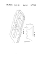
- FIG. 1 illustrates the magnetic coupling between two closely spaced magnetostatic wave devices that arises from the interaction of the magnetic field of one with the magnetic dipoles in the other.
- FIG. 2 is a top view of a pair of one port resonators coupled in the manner illustrated in FIG. 1.
- FIG. 3 illustrates how a third magnetostatic device can be used to couple a first and second magnetostatic device.
- FIG. 4 illustrates that the magnetostatic wave devices can be coupled in a nonlinear arrangement.
- FIG. 5 illustrates the wide band filter response S 21 that can be achieved by coupling together a plurality of resonators having closely spaced fundamental resonant frequencies.
- the first digit of the reference numerals indicates the first figure in which the element indicated by that reference numeral is depicted.
- the reference numerals of analogous elements in different figures will have the same second digit.
- FIG. 1 is illustrated a new type of coupling between two or more magnetostatic wave devices without use of interconnecting conductors.
- a dielectric material such as gadolinium gallium garnet, quartz or sapphire
- blocks 12 and 13 of a thin film of a ferromagnetic material, such a yttrium-iron-garnet (YIG).
- Blocks 12 and 13 can be formed by cutting these blocks from a thin YIG film by use of a wafer saw and then mounting them on substrate 11 or they can be formed by growing by liquid phase epitaxy (LPE) a thin YIG film on the gadolinium gallium garnet and then patterning it by photolithographic techniques to produce blocks 12 and 13. This latter method is preferred because of the ease of manufacture, the accuracy of alignment of the blocks and the smoothness of the edges of the blocks.
- LPE liquid phase epitaxy
- the distance D will typically be on the order of or greater than 100 microns.
- An anisotropic etch process can be used to etch walls 14 and 15, but such an anisotropic etch process would take a much longer time than an isotropic chemical etch and therefore will generally not be the preferred method of forming blocks 12 and 13. However, in embodiments in which a spacing closer than 100 microns is required, an anisotropic etch process could be used.
- the lengths L of the YIG blocks are on the order of 800-1000 microns and the widths W of the YIG blocks are on the order of 2000-3000 microns so that the spacing between the blocks is typically much smaller than the wavelength of the fundamental resonant modes of the YIG blocks. As a result of this, there is a very strong coupling between the two blocks.
- the spacing between the blocks is selected to be on the order of or less than a few times the wavelength of the fundamental mode of each block and is preferrably selected to be less than 1/16 of the wavelength of the fundamental mode to achieve strong coupling.
- FIG. 2 is illustrated an embodiment in which a pair of one port resonators are coupled together in the manner illustrated in FIG. 1.
- a first resonator (consisting of a block 22 of YIG film and a microstrip tranducer 26) and a second resonator (consisting of a block 23 of YIG film and a microstrip transducer 27) are positioned with closely spaced edges 24 and 25.
- This combination functions as a two port resonator in which transducer 26 functions as the input port and transducer 27 functions as the output port.
- transducer 26 not only generates magnetostatic waves in block 26, it also generates radio waves that can interact directly with transducer 27. Such direct action is a spurious coupling between these two transducers that does not exhibit the resonant behavior produced by the magnetostatic waves in blocks 22 and 23. Because of the relatively close spaing of the first and second resonators, this direct coupling will be more significant than in previous coupling methods in which the first and second resonators will generally be spaced at a greater distance.
- the first resonator consists of a block 32 of YIG film and a microstrip transducer 36.
- the second resonator consists of a clock 33 of YIG film and a microstrip transducer 37.
- An additional block 38 of YIG film is located between blocks 32 and 33 to couple the first resonator to the second resonator.
- a first end 39 of block 38 is positioned close to an end 34 of block 32 in order to couple the signal from block 32 into block 38.
- a second end 39' of block 38 is positioned close to an end 35 of block 33 to couple the signal from block 38 into block 33.
- the spacing S' between transducers 36 and 37 is much greater than the spacing between transducers 26 and 27 in FIG. 2 so that the direct electromagnetic wave coupling, which drops off roughly as the inverse square of the distance between the transducers, is significantly reduced in the embodiment of FIG. 3 compared to the embodiment in FIG. 2.
- FIG. 4 is presented a magnetostatic wave device in which a magnetostatic wave delay line (consisting of a block 42 of YIG film and a transducer 46) is coupled in a nonlinear arrangement to a magnetostatic wave resonator (consisting of a flock 43 of YIG film and a microstrip transducer 47).
- the delay line includes an absorbing medium 49, such as a thin coating of metal particles, to absorb magnetostatic waves travelling toward an end 49' of the magnetostatic wave delay line. Therefore, an input signal at transducer 46 launches a magnetostatic wave I in block 42 in the direction indicated by arrow 410.
- This magnetostatic wave I launches a magnetostatic waves in YIG block 48 and these magnetostatic waves in turn induce magnetostatic waves in block 43.
- This embodiment illustrates that different types of magnetostatic wave devices can be coupled together by the coupling illustrated in FIG. 1 and also illustrates that such couplings need not be in a strictly linear arrangement.
- FIG. 5 is presented a plot of the transfer function S 21 between input transducer 36 and output transducer 37 as a function of the frequency f of a sinusoidal signal V applied to input transducer 36.
- ⁇ f k is the halfwidth of the kth resonant peak.
- the adjacent edges of adjacent blocks are generally aligned to be substantially parallel. Because of this, waves travelling substantially perpendicular to edge 14 in Figure 1 launch waves in block 13 substantially perpendicular to edge 15.
- blocks 12 and 13 have the same length and width, a given mode of wave in block 12 will stimulate the same mode in block 13.
Landscapes
- Control Of Motors That Do Not Use Commutators (AREA)
- Surface Acoustic Wave Elements And Circuit Networks Thereof (AREA)
Priority Applications (3)
| Application Number | Priority Date | Filing Date | Title |
|---|---|---|---|
| US07/094,959 US4777462A (en) | 1987-09-09 | 1987-09-09 | Edge coupler magnetostatic wave structures |
| JP63223346A JPS6484905A (en) | 1987-09-09 | 1988-09-06 | Magnetostatic wave coupling device |
| EP88308298A EP0307196A3 (de) | 1987-09-09 | 1988-09-08 | Randgekoppelte magnetostatische Wellenstrukturen |
Applications Claiming Priority (1)
| Application Number | Priority Date | Filing Date | Title |
|---|---|---|---|
| US07/094,959 US4777462A (en) | 1987-09-09 | 1987-09-09 | Edge coupler magnetostatic wave structures |
Publications (1)
| Publication Number | Publication Date |
|---|---|
| US4777462A true US4777462A (en) | 1988-10-11 |
Family
ID=22248175
Family Applications (1)
| Application Number | Title | Priority Date | Filing Date |
|---|---|---|---|
| US07/094,959 Expired - Fee Related US4777462A (en) | 1987-09-09 | 1987-09-09 | Edge coupler magnetostatic wave structures |
Country Status (3)
| Country | Link |
|---|---|
| US (1) | US4777462A (de) |
| EP (1) | EP0307196A3 (de) |
| JP (1) | JPS6484905A (de) |
Cited By (6)
| Publication number | Priority date | Publication date | Assignee | Title |
|---|---|---|---|---|
| US4939488A (en) * | 1987-05-06 | 1990-07-03 | Murata Manufacturing Co., Ltd. | Magnetostatic wave device |
| US4983937A (en) * | 1988-07-20 | 1991-01-08 | Hitachi, Ltd. | Magnetostatic wave band-pass-filter |
| US4998080A (en) * | 1989-06-02 | 1991-03-05 | Polytechnic University | Microwave channelizer based on coupled YIG resonators |
| US5191308A (en) * | 1990-01-19 | 1993-03-02 | Murata Manufacturing Co., Ltd. | Magnetostrictive wave device having a higher maximum cut-off band elimination filter |
| US5371482A (en) * | 1991-10-16 | 1994-12-06 | Hitachi Metals, Ltd. | Magnetostatic wave device containing acoustic wave absorbing layer |
| US6816038B2 (en) * | 2000-11-22 | 2004-11-09 | Sanyo Electric Co., Ltd. | Magnetostatic wave device and disturbance wave eliminator |
Families Citing this family (1)
| Publication number | Priority date | Publication date | Assignee | Title |
|---|---|---|---|---|
| CN107017470A (zh) * | 2017-04-12 | 2017-08-04 | 电子科技大学 | 一种基于强互耦效应的低剖面宽带宽角扫描相控阵天线 |
Citations (2)
| Publication number | Priority date | Publication date | Assignee | Title |
|---|---|---|---|---|
| US4314214A (en) * | 1979-07-06 | 1982-02-02 | Thomson-Csf | Magnetostatic-wave device comprising a conducting strip exchange structure |
| US4528529A (en) * | 1983-12-12 | 1985-07-09 | Hewlett-Packard Company | Magnetostatic wave resonator |
Family Cites Families (1)
| Publication number | Priority date | Publication date | Assignee | Title |
|---|---|---|---|---|
| US4595889A (en) * | 1984-11-27 | 1986-06-17 | The United States Of America As Represented By The Secretary Of The Air Force | Frequency selective signal-to-noise enhancer/limiter apparatus |
-
1987
- 1987-09-09 US US07/094,959 patent/US4777462A/en not_active Expired - Fee Related
-
1988
- 1988-09-06 JP JP63223346A patent/JPS6484905A/ja active Pending
- 1988-09-08 EP EP88308298A patent/EP0307196A3/de not_active Withdrawn
Patent Citations (2)
| Publication number | Priority date | Publication date | Assignee | Title |
|---|---|---|---|---|
| US4314214A (en) * | 1979-07-06 | 1982-02-02 | Thomson-Csf | Magnetostatic-wave device comprising a conducting strip exchange structure |
| US4528529A (en) * | 1983-12-12 | 1985-07-09 | Hewlett-Packard Company | Magnetostatic wave resonator |
Non-Patent Citations (4)
| Title |
|---|
| "Compact Magnetostatic Wave Channelizer" by Michael R. Daniel and J. D. Adam, 1986 IEEE MTT-S International Microwave Symposium Digest, p. 481. |
| "Tunable Magnetostatic Volume Wave Oscillator" by J. P. Casters, et al., IEEE MTT-S International Microwave Symposium Digest (1983). |
| Compact Magnetostatic Wave Channelizer by Michael R. Daniel and J. D. Adam, 1986 IEEE MTT S International Microwave Symposium Digest, p. 481. * |
| Tunable Magnetostatic Volume Wave Oscillator by J. P. Casters, et al., IEEE MTT S International Microwave Symposium Digest (1983). * |
Cited By (6)
| Publication number | Priority date | Publication date | Assignee | Title |
|---|---|---|---|---|
| US4939488A (en) * | 1987-05-06 | 1990-07-03 | Murata Manufacturing Co., Ltd. | Magnetostatic wave device |
| US4983937A (en) * | 1988-07-20 | 1991-01-08 | Hitachi, Ltd. | Magnetostatic wave band-pass-filter |
| US4998080A (en) * | 1989-06-02 | 1991-03-05 | Polytechnic University | Microwave channelizer based on coupled YIG resonators |
| US5191308A (en) * | 1990-01-19 | 1993-03-02 | Murata Manufacturing Co., Ltd. | Magnetostrictive wave device having a higher maximum cut-off band elimination filter |
| US5371482A (en) * | 1991-10-16 | 1994-12-06 | Hitachi Metals, Ltd. | Magnetostatic wave device containing acoustic wave absorbing layer |
| US6816038B2 (en) * | 2000-11-22 | 2004-11-09 | Sanyo Electric Co., Ltd. | Magnetostatic wave device and disturbance wave eliminator |
Also Published As
| Publication number | Publication date |
|---|---|
| EP0307196A2 (de) | 1989-03-15 |
| JPS6484905A (en) | 1989-03-30 |
| EP0307196A3 (de) | 1990-02-28 |
Similar Documents
| Publication | Publication Date | Title |
|---|---|---|
| Adam et al. | Microwave magnetostatic delay devices based on epitaxial yttrium iron garnet | |
| US4318061A (en) | Tunable microwave oscillator using magnetostatic waves | |
| Castera | State of the art in design and technology of MSW devices | |
| RU96108787A (ru) | Тонкопленочный многослойный электрод со связью по высокочастотному электромагнитному полю | |
| US4199737A (en) | Magnetostatic wave device | |
| Demidov et al. | Electrical tuning of dispersion characteristics of surface electromagnetic-spin waves propagating in ferrite-ferroelectric layered structures | |
| US4777462A (en) | Edge coupler magnetostatic wave structures | |
| US4188594A (en) | Fixed frequency filters using epitaxial ferrite films | |
| US4751480A (en) | One port magnetostatic wave resonator | |
| Owens et al. | Magnetostatic wave propagation through periodic metallic gratings | |
| Castera et al. | Adjustable magnetostatic surface-wave multistrip directional coupler | |
| Tsutsumi et al. | The magnetostatic surface‐wave propagation in a corrugated YIG slab | |
| Merry et al. | Low loss magnetostatic surface waves at frequencies up to 15 GHz | |
| Adam et al. | Microwave device applications of epitaxial magnetic garnets | |
| US4716390A (en) | Magnetostatic wave channelizer | |
| US4472692A (en) | Tunable selective device using magnetostatic bulk waves | |
| US3530409A (en) | Two-port magnetoelastic delay line | |
| Hartemann | Magnetostatic wave planar YIG devices | |
| US4571562A (en) | Tunable selective devices based for magnetostatic volume waves | |
| US5189383A (en) | Circuit element utilizing magnetostatic wave | |
| US5017896A (en) | Mode trapped magnetostatic wave (MSW) filters and channelizer formed therefrom | |
| JP2636580B2 (ja) | 静磁波装置 | |
| US5168254A (en) | Magnetostatic wave device with minimized higher order mode excitations | |
| US5371482A (en) | Magnetostatic wave device containing acoustic wave absorbing layer | |
| US4774483A (en) | Diagonally coupled magnetostatic wave resonators |
Legal Events
| Date | Code | Title | Description |
|---|---|---|---|
| AS | Assignment |
Owner name: HEWLETT-PACKARD COMPANY,CALIFORNIA Free format text: ASSIGNMENT OF ASSIGNORS INTEREST;ASSIGNORS:KUNZ, WILLIAM E.;CHANG, KOK W.;MICCOLI, GIUSEPPE;SIGNING DATES FROM 19870827 TO 19870904;REEL/FRAME:004770/0968 Owner name: HEWLETT-PACKARD COMPANY, PALO ALTO, CA. A CORP. OF Free format text: ASSIGNMENT OF ASSIGNORS INTEREST.;ASSIGNORS:KUNZ, WILLIAM E.;CHANG, KOK W.;MICCOLI, GIUSEPPE;REEL/FRAME:004770/0968;SIGNING DATES FROM 19870827 TO 19870904 |
|
| FEPP | Fee payment procedure |
Free format text: PAYOR NUMBER ASSIGNED (ORIGINAL EVENT CODE: ASPN); ENTITY STATUS OF PATENT OWNER: LARGE ENTITY |
|
| FPAY | Fee payment |
Year of fee payment: 4 |
|
| REMI | Maintenance fee reminder mailed | ||
| LAPS | Lapse for failure to pay maintenance fees | ||
| FP | Lapsed due to failure to pay maintenance fee |
Effective date: 19961016 |
|
| STCH | Information on status: patent discontinuation |
Free format text: PATENT EXPIRED DUE TO NONPAYMENT OF MAINTENANCE FEES UNDER 37 CFR 1.362 |