EP0300516A2 - Digitales Datenverarbeitungssystem - Google Patents
Digitales Datenverarbeitungssystem Download PDFInfo
- Publication number
- EP0300516A2 EP0300516A2 EP88200921A EP88200921A EP0300516A2 EP 0300516 A2 EP0300516 A2 EP 0300516A2 EP 88200921 A EP88200921 A EP 88200921A EP 88200921 A EP88200921 A EP 88200921A EP 0300516 A2 EP0300516 A2 EP 0300516A2
- Authority
- EP
- European Patent Office
- Prior art keywords
- mem
- procedure
- data
- computer system
- digital computer
- Prior art date
- Legal status (The legal status is an assumption and is not a legal conclusion. Google has not performed a legal analysis and makes no representation as to the accuracy of the status listed.)
- Granted
Links
- 238000012545 processing Methods 0.000 title abstract description 58
- 230000015654 memory Effects 0.000 claims abstract description 1306
- 230000004224 protection Effects 0.000 claims abstract description 149
- 238000000034 method Methods 0.000 claims description 1423
- 230000008569 process Effects 0.000 claims description 642
- 230000004044 response Effects 0.000 claims description 34
- 238000012790 confirmation Methods 0.000 claims description 2
- 238000012546 transfer Methods 0.000 description 268
- 230000007246 mechanism Effects 0.000 description 229
- 238000010586 diagram Methods 0.000 description 144
- 230000014616 translation Effects 0.000 description 108
- 238000013519 translation Methods 0.000 description 107
- 230000006870 function Effects 0.000 description 97
- 230000001404 mediated effect Effects 0.000 description 80
- 230000003068 static effect Effects 0.000 description 51
- 238000006073 displacement reaction Methods 0.000 description 48
- 238000007726 management method Methods 0.000 description 48
- 239000000872 buffer Substances 0.000 description 47
- 238000011068 loading method Methods 0.000 description 46
- 238000012360 testing method Methods 0.000 description 41
- 230000036961 partial effect Effects 0.000 description 40
- 238000011156 evaluation Methods 0.000 description 28
- 239000005020 polyethylene terephthalate Substances 0.000 description 24
- 229920000139 polyethylene terephthalate Polymers 0.000 description 24
- 230000000873 masking effect Effects 0.000 description 23
- 230000008859 change Effects 0.000 description 20
- 230000027455 binding Effects 0.000 description 18
- 238000009739 binding Methods 0.000 description 18
- 230000000977 initiatory effect Effects 0.000 description 18
- 239000011230 binding agent Substances 0.000 description 17
- 230000001133 acceleration Effects 0.000 description 15
- 230000009471 action Effects 0.000 description 14
- 238000003491 array Methods 0.000 description 14
- BXMVKQIIJSXIBU-UHFFFAOYSA-N (2,5-dioxopyrrolidin-1-yl) diphenyl phosphate Chemical compound O=C1CCC(=O)N1OP(=O)(OC=1C=CC=CC=1)OC1=CC=CC=C1 BXMVKQIIJSXIBU-UHFFFAOYSA-N 0.000 description 12
- 238000001514 detection method Methods 0.000 description 12
- 238000004891 communication Methods 0.000 description 11
- 238000005192 partition Methods 0.000 description 11
- 238000006243 chemical reaction Methods 0.000 description 10
- 238000012937 correction Methods 0.000 description 10
- 238000013507 mapping Methods 0.000 description 10
- 230000008439 repair process Effects 0.000 description 10
- 238000013500 data storage Methods 0.000 description 9
- 230000000694 effects Effects 0.000 description 9
- 230000009977 dual effect Effects 0.000 description 8
- 210000002592 gangliocyte Anatomy 0.000 description 7
- 238000012544 monitoring process Methods 0.000 description 7
- 230000002093 peripheral effect Effects 0.000 description 7
- 101100521334 Mus musculus Prom1 gene Proteins 0.000 description 6
- 230000001419 dependent effect Effects 0.000 description 6
- HJUFTIJOISQSKQ-UHFFFAOYSA-N fenoxycarb Chemical compound C1=CC(OCCNC(=O)OCC)=CC=C1OC1=CC=CC=C1 HJUFTIJOISQSKQ-UHFFFAOYSA-N 0.000 description 6
- 239000000796 flavoring agent Substances 0.000 description 6
- 235000019634 flavors Nutrition 0.000 description 6
- ZXQYGBMAQZUVMI-GCMPRSNUSA-N gamma-cyhalothrin Chemical compound CC1(C)[C@@H](\C=C(/Cl)C(F)(F)F)[C@H]1C(=O)O[C@H](C#N)C1=CC=CC(OC=2C=CC=CC=2)=C1 ZXQYGBMAQZUVMI-GCMPRSNUSA-N 0.000 description 6
- 230000000717 retained effect Effects 0.000 description 6
- 206010000210 abortion Diseases 0.000 description 5
- 230000006399 behavior Effects 0.000 description 5
- 238000004422 calculation algorithm Methods 0.000 description 5
- 238000004364 calculation method Methods 0.000 description 5
- 230000003111 delayed effect Effects 0.000 description 5
- 239000000284 extract Substances 0.000 description 5
- 238000011010 flushing procedure Methods 0.000 description 5
- 238000012423 maintenance Methods 0.000 description 5
- 239000011159 matrix material Substances 0.000 description 5
- 230000008520 organization Effects 0.000 description 5
- 230000002441 reversible effect Effects 0.000 description 5
- 230000004913 activation Effects 0.000 description 4
- 230000001934 delay Effects 0.000 description 4
- 230000001965 increasing effect Effects 0.000 description 4
- RZVAJINKPMORJF-UHFFFAOYSA-N Acetaminophen Chemical compound CC(=O)NC1=CC=C(O)C=C1 RZVAJINKPMORJF-UHFFFAOYSA-N 0.000 description 3
- 230000002708 enhancing effect Effects 0.000 description 3
- 238000011049 filling Methods 0.000 description 3
- 241000208479 Anagallis arvensis Species 0.000 description 2
- 240000006766 Cornus mas Species 0.000 description 2
- 230000003466 anti-cipated effect Effects 0.000 description 2
- 230000008901 benefit Effects 0.000 description 2
- 230000005540 biological transmission Effects 0.000 description 2
- 238000010276 construction Methods 0.000 description 2
- 238000002405 diagnostic procedure Methods 0.000 description 2
- 238000003780 insertion Methods 0.000 description 2
- 230000037431 insertion Effects 0.000 description 2
- 238000012986 modification Methods 0.000 description 2
- 230000004048 modification Effects 0.000 description 2
- 238000010606 normalization Methods 0.000 description 2
- 239000005022 packaging material Substances 0.000 description 2
- 238000012856 packing Methods 0.000 description 2
- 230000000704 physical effect Effects 0.000 description 2
- 229920002745 polystyrene-block- poly(ethylene /butylene) Polymers 0.000 description 2
- 238000001650 pulsed electrochemical detection Methods 0.000 description 2
- 230000002829 reductive effect Effects 0.000 description 2
- 230000001360 synchronised effect Effects 0.000 description 2
- 230000026676 system process Effects 0.000 description 2
- 230000009466 transformation Effects 0.000 description 2
- 230000007704 transition Effects 0.000 description 2
- 102100028626 4-hydroxyphenylpyruvate dioxygenase Human genes 0.000 description 1
- 108010031096 8-amino-7-oxononanoate synthase Proteins 0.000 description 1
- 101710163391 ADP-ribosyl cyclase/cyclic ADP-ribose hydrolase Proteins 0.000 description 1
- 208000035708 Autosomal dominant striatal neurodegeneration Diseases 0.000 description 1
- 208000009766 Blau syndrome Diseases 0.000 description 1
- 102100040862 Dual specificity protein kinase CLK1 Human genes 0.000 description 1
- 101000749294 Homo sapiens Dual specificity protein kinase CLK1 Proteins 0.000 description 1
- 101100007538 Neurospora crassa (strain ATCC 24698 / 74-OR23-1A / CBS 708.71 / DSM 1257 / FGSC 987) cpc-1 gene Proteins 0.000 description 1
- 102000010410 Nogo Proteins Human genes 0.000 description 1
- 108010077641 Nogo Proteins Proteins 0.000 description 1
- 108091081062 Repeated sequence (DNA) Proteins 0.000 description 1
- 230000003213 activating effect Effects 0.000 description 1
- 230000003044 adaptive effect Effects 0.000 description 1
- 238000013459 approach Methods 0.000 description 1
- 208000036182 autosomal dominant striatal degeneration Diseases 0.000 description 1
- 210000004027 cell Anatomy 0.000 description 1
- 230000000295 complement effect Effects 0.000 description 1
- 238000004590 computer program Methods 0.000 description 1
- 239000012141 concentrate Substances 0.000 description 1
- 239000000470 constituent Substances 0.000 description 1
- 230000009849 deactivation Effects 0.000 description 1
- 238000012217 deletion Methods 0.000 description 1
- 230000037430 deletion Effects 0.000 description 1
- 238000011161 development Methods 0.000 description 1
- 230000007613 environmental effect Effects 0.000 description 1
- 238000000605 extraction Methods 0.000 description 1
- 230000014509 gene expression Effects 0.000 description 1
- 230000006872 improvement Effects 0.000 description 1
- 230000002401 inhibitory effect Effects 0.000 description 1
- 230000002452 interceptive effect Effects 0.000 description 1
- 238000002955 isolation Methods 0.000 description 1
- 230000002045 lasting effect Effects 0.000 description 1
- 230000000670 limiting effect Effects 0.000 description 1
- 230000014759 maintenance of location Effects 0.000 description 1
- 230000005055 memory storage Effects 0.000 description 1
- YFBPRJGDJKVWAH-UHFFFAOYSA-N methiocarb Chemical compound CNC(=O)OC1=CC(C)=C(SC)C(C)=C1 YFBPRJGDJKVWAH-UHFFFAOYSA-N 0.000 description 1
- 239000000203 mixture Substances 0.000 description 1
- FFNMBRCFFADNAO-UHFFFAOYSA-N pirenzepine hydrochloride Chemical compound [H+].[H+].[Cl-].[Cl-].C1CN(C)CCN1CC(=O)N1C2=NC=CC=C2NC(=O)C2=CC=CC=C21 FFNMBRCFFADNAO-UHFFFAOYSA-N 0.000 description 1
- 229920002469 poly(p-dioxane) polymer Polymers 0.000 description 1
- 230000002028 premature Effects 0.000 description 1
- 238000000899 pressurised-fluid extraction Methods 0.000 description 1
- 230000003252 repetitive effect Effects 0.000 description 1
- 238000013468 resource allocation Methods 0.000 description 1
- 238000004092 self-diagnosis Methods 0.000 description 1
- 239000004065 semiconductor Substances 0.000 description 1
- 230000011664 signaling Effects 0.000 description 1
- 239000007787 solid Substances 0.000 description 1
- 238000000638 solvent extraction Methods 0.000 description 1
- 238000006467 substitution reaction Methods 0.000 description 1
- 239000000725 suspension Substances 0.000 description 1
- 238000000844 transformation Methods 0.000 description 1
- 230000001131 transforming effect Effects 0.000 description 1
- 238000013024 troubleshooting Methods 0.000 description 1
- 239000013598 vector Substances 0.000 description 1
Images


Classifications
-
- G—PHYSICS
- G06—COMPUTING; CALCULATING OR COUNTING
- G06F—ELECTRIC DIGITAL DATA PROCESSING
- G06F11/00—Error detection; Error correction; Monitoring
- G06F11/07—Responding to the occurrence of a fault, e.g. fault tolerance
- G06F11/0703—Error or fault processing not based on redundancy, i.e. by taking additional measures to deal with the error or fault not making use of redundancy in operation, in hardware, or in data representation
- G06F11/0793—Remedial or corrective actions
-
- G—PHYSICS
- G01—MEASURING; TESTING
- G01R—MEASURING ELECTRIC VARIABLES; MEASURING MAGNETIC VARIABLES
- G01R31/00—Arrangements for testing electric properties; Arrangements for locating electric faults; Arrangements for electrical testing characterised by what is being tested not provided for elsewhere
- G01R31/28—Testing of electronic circuits, e.g. by signal tracer
- G01R31/317—Testing of digital circuits
- G01R31/3181—Functional testing
- G01R31/3185—Reconfiguring for testing, e.g. LSSD, partitioning
- G01R31/318505—Test of Modular systems, e.g. Wafers, MCM's
-
- G—PHYSICS
- G06—COMPUTING; CALCULATING OR COUNTING
- G06F—ELECTRIC DIGITAL DATA PROCESSING
- G06F11/00—Error detection; Error correction; Monitoring
- G06F11/07—Responding to the occurrence of a fault, e.g. fault tolerance
- G06F11/0703—Error or fault processing not based on redundancy, i.e. by taking additional measures to deal with the error or fault not making use of redundancy in operation, in hardware, or in data representation
- G06F11/0706—Error or fault processing not based on redundancy, i.e. by taking additional measures to deal with the error or fault not making use of redundancy in operation, in hardware, or in data representation the processing taking place on a specific hardware platform or in a specific software environment
- G06F11/0721—Error or fault processing not based on redundancy, i.e. by taking additional measures to deal with the error or fault not making use of redundancy in operation, in hardware, or in data representation the processing taking place on a specific hardware platform or in a specific software environment within a central processing unit [CPU]
-
- G—PHYSICS
- G06—COMPUTING; CALCULATING OR COUNTING
- G06F—ELECTRIC DIGITAL DATA PROCESSING
- G06F11/00—Error detection; Error correction; Monitoring
- G06F11/07—Responding to the occurrence of a fault, e.g. fault tolerance
- G06F11/0703—Error or fault processing not based on redundancy, i.e. by taking additional measures to deal with the error or fault not making use of redundancy in operation, in hardware, or in data representation
- G06F11/0706—Error or fault processing not based on redundancy, i.e. by taking additional measures to deal with the error or fault not making use of redundancy in operation, in hardware, or in data representation the processing taking place on a specific hardware platform or in a specific software environment
- G06F11/073—Error or fault processing not based on redundancy, i.e. by taking additional measures to deal with the error or fault not making use of redundancy in operation, in hardware, or in data representation the processing taking place on a specific hardware platform or in a specific software environment in a memory management context, e.g. virtual memory or cache management
-
- G—PHYSICS
- G06—COMPUTING; CALCULATING OR COUNTING
- G06F—ELECTRIC DIGITAL DATA PROCESSING
- G06F12/00—Accessing, addressing or allocating within memory systems or architectures
- G06F12/02—Addressing or allocation; Relocation
- G06F12/08—Addressing or allocation; Relocation in hierarchically structured memory systems, e.g. virtual memory systems
- G06F12/0802—Addressing of a memory level in which the access to the desired data or data block requires associative addressing means, e.g. caches
- G06F12/0875—Addressing of a memory level in which the access to the desired data or data block requires associative addressing means, e.g. caches with dedicated cache, e.g. instruction or stack
-
- G—PHYSICS
- G06—COMPUTING; CALCULATING OR COUNTING
- G06F—ELECTRIC DIGITAL DATA PROCESSING
- G06F12/00—Accessing, addressing or allocating within memory systems or architectures
- G06F12/14—Protection against unauthorised use of memory or access to memory
- G06F12/1458—Protection against unauthorised use of memory or access to memory by checking the subject access rights
- G06F12/1483—Protection against unauthorised use of memory or access to memory by checking the subject access rights using an access-table, e.g. matrix or list
-
- G—PHYSICS
- G06—COMPUTING; CALCULATING OR COUNTING
- G06F—ELECTRIC DIGITAL DATA PROCESSING
- G06F7/00—Methods or arrangements for processing data by operating upon the order or content of the data handled
-
- G—PHYSICS
- G06—COMPUTING; CALCULATING OR COUNTING
- G06F—ELECTRIC DIGITAL DATA PROCESSING
- G06F7/00—Methods or arrangements for processing data by operating upon the order or content of the data handled
- G06F7/38—Methods or arrangements for performing computations using exclusively denominational number representation, e.g. using binary, ternary, decimal representation
- G06F7/48—Methods or arrangements for performing computations using exclusively denominational number representation, e.g. using binary, ternary, decimal representation using non-contact-making devices, e.g. tube, solid state device; using unspecified devices
- G06F7/483—Computations with numbers represented by a non-linear combination of denominational numbers, e.g. rational numbers, logarithmic number system or floating-point numbers
-
- G—PHYSICS
- G06—COMPUTING; CALCULATING OR COUNTING
- G06F—ELECTRIC DIGITAL DATA PROCESSING
- G06F9/00—Arrangements for program control, e.g. control units
- G06F9/06—Arrangements for program control, e.g. control units using stored programs, i.e. using an internal store of processing equipment to receive or retain programs
- G06F9/22—Microcontrol or microprogram arrangements
- G06F9/223—Execution means for microinstructions irrespective of the microinstruction function, e.g. decoding of microinstructions and nanoinstructions; timing of microinstructions; programmable logic arrays; delays and fan-out problems
-
- G—PHYSICS
- G06—COMPUTING; CALCULATING OR COUNTING
- G06F—ELECTRIC DIGITAL DATA PROCESSING
- G06F9/00—Arrangements for program control, e.g. control units
- G06F9/06—Arrangements for program control, e.g. control units using stored programs, i.e. using an internal store of processing equipment to receive or retain programs
- G06F9/22—Microcontrol or microprogram arrangements
- G06F9/226—Microinstruction function, e.g. input/output microinstruction; diagnostic microinstruction; microinstruction format
-
- G—PHYSICS
- G06—COMPUTING; CALCULATING OR COUNTING
- G06F—ELECTRIC DIGITAL DATA PROCESSING
- G06F9/00—Arrangements for program control, e.g. control units
- G06F9/06—Arrangements for program control, e.g. control units using stored programs, i.e. using an internal store of processing equipment to receive or retain programs
- G06F9/22—Microcontrol or microprogram arrangements
- G06F9/26—Address formation of the next micro-instruction ; Microprogram storage or retrieval arrangements
- G06F9/262—Arrangements for next microinstruction selection
- G06F9/268—Microinstruction selection not based on processing results, e.g. interrupt, patch, first cycle store, diagnostic programs
-
- G—PHYSICS
- G06—COMPUTING; CALCULATING OR COUNTING
- G06F—ELECTRIC DIGITAL DATA PROCESSING
- G06F9/00—Arrangements for program control, e.g. control units
- G06F9/06—Arrangements for program control, e.g. control units using stored programs, i.e. using an internal store of processing equipment to receive or retain programs
- G06F9/30—Arrangements for executing machine instructions, e.g. instruction decode
- G06F9/34—Addressing or accessing the instruction operand or the result ; Formation of operand address; Addressing modes
- G06F9/35—Indirect addressing
-
- G—PHYSICS
- G06—COMPUTING; CALCULATING OR COUNTING
- G06F—ELECTRIC DIGITAL DATA PROCESSING
- G06F9/00—Arrangements for program control, e.g. control units
- G06F9/06—Arrangements for program control, e.g. control units using stored programs, i.e. using an internal store of processing equipment to receive or retain programs
- G06F9/44—Arrangements for executing specific programs
- G06F9/448—Execution paradigms, e.g. implementations of programming paradigms
- G06F9/4488—Object-oriented
-
- G—PHYSICS
- G06—COMPUTING; CALCULATING OR COUNTING
- G06F—ELECTRIC DIGITAL DATA PROCESSING
- G06F9/00—Arrangements for program control, e.g. control units
- G06F9/06—Arrangements for program control, e.g. control units using stored programs, i.e. using an internal store of processing equipment to receive or retain programs
- G06F9/46—Multiprogramming arrangements
- G06F9/468—Specific access rights for resources, e.g. using capability register
-
- G—PHYSICS
- G06—COMPUTING; CALCULATING OR COUNTING
- G06F—ELECTRIC DIGITAL DATA PROCESSING
- G06F9/00—Arrangements for program control, e.g. control units
- G06F9/06—Arrangements for program control, e.g. control units using stored programs, i.e. using an internal store of processing equipment to receive or retain programs
- G06F9/46—Multiprogramming arrangements
- G06F9/48—Program initiating; Program switching, e.g. by interrupt
- G06F9/4806—Task transfer initiation or dispatching
- G06F9/4843—Task transfer initiation or dispatching by program, e.g. task dispatcher, supervisor, operating system
-
- G—PHYSICS
- G06—COMPUTING; CALCULATING OR COUNTING
- G06F—ELECTRIC DIGITAL DATA PROCESSING
- G06F9/00—Arrangements for program control, e.g. control units
- G06F9/06—Arrangements for program control, e.g. control units using stored programs, i.e. using an internal store of processing equipment to receive or retain programs
- G06F9/46—Multiprogramming arrangements
- G06F9/54—Interprogram communication
-
- G—PHYSICS
- G06—COMPUTING; CALCULATING OR COUNTING
- G06F—ELECTRIC DIGITAL DATA PROCESSING
- G06F7/00—Methods or arrangements for processing data by operating upon the order or content of the data handled
- G06F7/38—Methods or arrangements for performing computations using exclusively denominational number representation, e.g. using binary, ternary, decimal representation
- G06F7/48—Methods or arrangements for performing computations using exclusively denominational number representation, e.g. using binary, ternary, decimal representation using non-contact-making devices, e.g. tube, solid state device; using unspecified devices
- G06F7/499—Denomination or exception handling, e.g. rounding or overflow
- G06F7/49905—Exception handling
- G06F7/4991—Overflow or underflow
-
- G—PHYSICS
- G06—COMPUTING; CALCULATING OR COUNTING
- G06F—ELECTRIC DIGITAL DATA PROCESSING
- G06F7/00—Methods or arrangements for processing data by operating upon the order or content of the data handled
- G06F7/38—Methods or arrangements for performing computations using exclusively denominational number representation, e.g. using binary, ternary, decimal representation
- G06F7/48—Methods or arrangements for performing computations using exclusively denominational number representation, e.g. using binary, ternary, decimal representation using non-contact-making devices, e.g. tube, solid state device; using unspecified devices
- G06F7/499—Denomination or exception handling, e.g. rounding or overflow
- G06F7/49905—Exception handling
- G06F7/49926—Division by zero
Definitions
- the present invention relates to a digital data processing system and, more particularly, to a multiprocessor digital data processing system suitable for use in a data processing network and having a simplified, flexible user interface and flexible, multileveled internal mechanisms.
- a general trend in the development of data processing systems has been towards systems suitable for use in interconnected data processing networks.
- Another trend has been towards data processing systems wherein the internal structures of the system is flexible, protected from users, and effectively invisible to the user and wherein the user is presented with a flexible and simplified interface to the system.
- the data processing systems of the prior art have not provided a system wide addressing system suitable for use in common by a large number of data processing systems interconnected into a network. Addressing systems of the prior art have not provided sufficiently large address spaces and have not allowed information to be permanently and uniquely identified. Prior addressing systems have not made provisions for information to be located and identified as to type or format, and have not provided sufficient granularity. In addition, prior addressing systems have reflected the physical structure of particular data processing systems. That is, the addressing systems have been dependent upon whether a particular computer was, for example, an 8, 16, 32, 64 or 128 bit machine. Since prior data processing systems have incorporated addressing mechanisms wherein the actual physical structure of the processing system is apparent to the user, the operations a user could perform have been limited by the addressing mechanisms. In addition, prior processor systems have operated as fixed word length machines, further limiting user operations.
- Prior data processing systems have not provided effective protection mechanisms preventing one' user from effecting another user's data and programs without permission.
- Such protection mechanisms have not allowed unique, positive identification of users requesting access to information, or of information, nor have such mechanisms been sufficiently flexible in operation.
- access rights have pertained to the users rather than to the information, so that control of access rights has been difficult.
- prior art protection mechanisms have allowed the use of "Trojan Horse arguments”. That is, users not having access rights to certain information have been able to gain access to that information through another user or procedure having such access rights.
- Yet another problem of the prior art is that of providing a simple and flexible interface user interface to a data processing system.
- the character of user's interface to a data processing system is determined, in part, by the means by which a user refers to and identifies operands and procedures of the user's programs and by the instruction structure of the system. Operands and procedures are customarily referred to and identified by some form of logical address having points of reference, and validity, only within a user's program. These addresses must be translated into logical and physical addresses within a data processing system each time a program is executed, and must then be frequently retranslated or generated during execution of a program. In addition, a user must provide specific instructions as to data format and handling.
- operands or procedures typically comprise a major portion of the instruction stream of the user's program and requires numerous machine translations and operations to implement.
- a user's interface to a conventional system is thereby complicated, and the speed of execution of programs reduced, because of the complexity of the program references to operands and procedures.
- a data processing system's instruction structure includes both the instructions for controlling system operations and the means by which these instructions are executed.
- Conventional data processing systems are designed to efficiently execute instructions in one or two user languages, for example, FORTRAN or COBOL. Programs written in any other language are not efficiently executable.
- a user is often faced with difficult programming problems when using any high level language other than the particular one or two languages that a particular conventional system is designed to utilize.
- Yet another problem in conventional data processing systems is that of protecting the system's internal mechanisms, for example, stack mechanisms and internal control mechanisms, from accidental or malicious interference by a user.
- the present invention provides data processing system improvements and features which solve the above-described problems and limitations.
- the present invention relates to structure and operation of a data processing system suitable for use in interconnected data processing networks, which internal structure is flexible, protected from users, effectively invisible to users, and provides a flexible and simplified interface to users.
- the data processing system provides an addressing mechanism allowing permanent and unique identification of all information generated for use in or by operation of the system, and an extremely large address space which is accessible to and common to all such data processing systems.
- the addressing mechanism provides addresses which are independent of the physical configuration of the system and allow information to be completely identified, with a single address, to the bit granular level and with regard to information type or format.
- the present invention further provides a protection mechanism wherein variable access rights are associated with individual bodies of information. Information, and users requesting access to information, are uniquely identified through the system addressing mechanism.
- the protection mechanism also prevents use of Trojan Horse arguments.
- the present invention provides an instruction structure wherein high level user language instructions are transformed into dialect coded, uniform, intermediate level instructions to provide equal facility of execution for a plurality of user languages.
- Another feature is the provision of an operand reference mechanism wherein operands are referred to in user's programs by uniform format names which are transformed, by an internal mechanism transparent to the user, into addresses.
- the present invention additionally provides multilevel control and stack mechanisms protecting the system's internal mechanism from interference by users.
- a data processing system having a flexible internal structure capable of performing multiple, concurrent operations and comprised of a plurality of separate, independent processors. Each such independent processor has a separate microinstruction control and at least one separate and independent port to a central communications and memory node.
- the communications and memory node is also an independent processor having separate and independent microinstruction control.
- the memory processor is internally comprised of a plurality of independently operating, microinstruction controlled processors capable of performing multipie, concurrent memory and communications operations.
- the present invention also provides further data processing system structural and operational features for implementing the above features.
- the present invention provides addressing mechanisms suitable for use in large interconnected data processing networks. Additionally, the present invention is advantageous in that it provides an information protection mechanism suitable for use in large, interconnected data processing networks. The present invention is further advantageous in that it provides a simplified, flexible, and more efficient interface to a data processing system. The present invention is yet further advantageous in that it provides a data processing system which is equally efficient with any user level language by providing a mechanism for referring to operands in user programs by uniform format names and instruction structure incorporating dialect coded, uniform format intermediate level instructions. Additionally, the present invention protects data processing system internal mechanisms from user interference by providing multilevel control and stack mechanisms.
- the present invention is yet further advantageous in providing a flexible internal system structure capable of performing multiple, concurrent operations, comprising a plurality of separate, independent processors, each having a separate microinstruction control and at least one separate and independent port to a central, independent communications and memory processor comprised of a plurality of independent processors capable of performing multiple, concurrent memory and communications operations.
- reference numerals comprise a two digit number (00-99) preceded by the number of the figure in which the corresponding elements first appear.
- reference numerals 31901 to 31999 would refer to elements 1 through 99 appearing in Fig. 319.
- interconnections between related circuitry is represented in two ways.
- reference numerals to elements will be assigned in sequence through the group of figures; the figure number portion of such reference numerals will be that of the first figure of the group of figures.
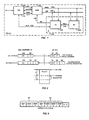
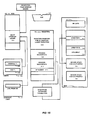
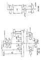
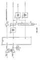
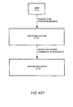
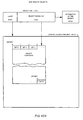
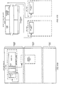
- CS 101 Computer System 101 incorporating the present invention is shown.
- IOS I/O System
- MEM Memory
- JP Job Processor
- JP 114 is comprised of a Fetch Unit (FU) 120 and an Execute Unit (EU) 122.
- CS 101 may also include a Diagnostic Processor (DP), not shown or described in the instant description.
- DP Diagnostic Processor
- IOS 116 a primary function of IOS 116 is control of transfer of information between MEM 112 and the outside world. Information is transferred from MEM 112 to IOS 116 through IOM Bus 130, and from IOS 116 to MEM 112 through MIO Bus 129.
- IOMC Bus 131 is comprised of bi-directional control signals coordinating operation of MEM 112 and IOS 116.
- IOS 116 also has an interface to FU 120 through IOJP Bus 132.
- IOJP Bus 132 is a bi-directional control bus comprised essentially of two interrupt lines. These interrupt lines allow FU 120 to indicate to IOS 116 that a request for information by FU 120 has been placed in MEM 112.
- MEM 112 is CS 101's main memory and serves as the path for information transfer between the outside world and JP 114.
- MEM 112 provides instructions and data to FU 120 and EU 122 through Memory Output Data (MOD) Bus 140 and receives information from FU 120 and EU 122 through Job Processor Data (JPD) Bus 142.
- FU 120 submits read and write requests to MEM 112 through Physical Descriptor (PD) Bus 146.
- JP 114 is CS 101's CPU and, as described above, is comprised of FU 120 and EU 122.
- a primary function of FU 120 is executing operations of user's programs. As part of this function, FU 120 controls transfer of instructions and data from MEM 112 and transfer of results of JP 114 operations back to MEM 112.
- FU 120 also performs operating system type functions, and is capable of operating as a complete, general purpose CPU.
- EU 122 is primarily an arithmetic and logic unit provided to relieve FU 120 of certain arithmetic operations. FU 120, however, is capable of performing EU 122 operations. In alternate embodiments of CS 101, EU 122 may be provided only as an option for users having particular arithmetic requirements.
- FU/EU Bus 148 which includes bi-directional control signals and mutual interrupt lines.
- FU 120 and EU 122 contain register file arrays referred to respectively as CRF and ERF, in addition to registers associated with, for example, ALUs.
- a primary feature of CS 101 is that IOS 116, MEM 112, FU 120 and EU 122 each contain separate and independent microinstruction control, so that IOS 116, MEM 112, and EU 122 operate asynchronously under the general control of FU 120.
- EU 122 may execute a complex arithmetic operation upon receipt of data and a single, initial command from FU 120.
- CS 101's addressing structure is based upon the concept of Objects.
- An Object may be regarded as a container for holding a particular type of information.
- one type of Object may contain data while another type of Object may contain instructions or procedures, such as a user program.
- Still another type of Object may contain microcode.
- a particular Object may contain only one type or class of information.
- An Object may, for example, contain up to 2 32 bits of information, but the actual size of a particular Object is flexible. That is, the actual size of a particular Object will increase as information is written into that Object and will decrease as information is taken from that Object.
- information in Objects is stored sequentially, that is without gaps. '
- UID Unique Identifier
- a UID is a 128 bit value comprised of a serial number dependent upon, for example, the particular CS 101 system and user, and a time code indicating time of creation of that Object.
- UIDs are permanently assigned to Objects, no two Objects may have the same UID, and UIDs may not be reused.
- UIDs provide an addressing base common to all CS 101 systems which may ever exist, through which any Object ever created may be permanently and uniquely identified.
- UIDs are 128 bit values and are thus larger than may be conveniently handled in present embodiments of CS 101.
- those Objects which are active (currently being used) in that system are assigned 14 bit Active Object Numbers (AONs).
- AONs Active Object Numbers
- Each Object active in that system will have a unique AON.
- UlDs Active Object Numbers
- AONs are only temporarily assigned to particular Objects. AONs are valid only within a particular CS 101 and are not unique between systems. An Object need not physically reside in a system to be assigned an AON, but can be active in that system only if it has been assigned an AON.
- a particular bit within a particular Object may be identified by means of a UID address or an AON address.
- AONs and AON addresses are valid only within JP 114 while UlDs and UID addresses are used in MEM 112 and elsewhere.
- UID and AON addresses are formed by appending a 32 bit Offset (0) field to that Object's UID or AON. 0 fields indicate offset, or location, of a particular bit relative to the start of a particular Object.
- Segments of information (sequences of information bits) within particular Objects may be identified by means of descriptors.
- a UID descriptor is formed by appending a 32 bit Length (L) field of a UID address.
- An AON, or logical descriptor is formed by appending a 32 bit L field to an AON address.
- L fields identify length of a segment of information bits within an Object, starting from the information bit identified by the UID or AON address.
- UID and logical descriptors also contain Type fields containing information regarding certain characteristics of the information in the information segment. Again, AON based descriptors are used within JP 114, while UID based descriptors are used in MEM 112.
- Figs. 1 and 2 translation between UID addresses and descriptors and AON addresses and descriptors is performed at the interface between MEM 112 and JP 114. That is, addresses and descriptors within JP 114 are in AON form while addresses and descriptors in MEM 112, IOS 116, and the external world are in UID form.
- transformation from UID to AON addressing may occur at other interfaces, for example at the IOS 116 to MEM 112 interface, or at the IOS 116 to external world interface.
- Other embodiments of CS 101 may use UIDs throughout, that is not use AONs even in JP 114.
- MEM 112 Physical Addresses identifying particular physical locations within MEM 112's memory space.
- IOS 116 and JP 114 address information within MEM 112 by providing physical addresses to MEM 112. In the case of physical addresses provided by JP 114, these addresses are referred to as Physical Descriptors (PDs).
- PDs Physical Descriptors
- JP 114 contains circuitry to translate logical descriptors into physical descriptors.
- CS 101 is both an S-Language machine and a Namespace machine. That is, operations to be executed by CS 101 are expressed as S-Language Operations (SOPs) while operands are identified by Names.
- SOPs are of a lower, more detailed, level than user language instructions, for example FORTRAN and COBOL, but of a higher level than conventional machine language instructions.
- SOPs are specific to particular user languages rather than a particular embodiment of CS 101, while conventional machine language instructions are specific to particular machines.
- SOPs are in turn interpreted and executed by microcode. There will be an S-Language Dialect, a set of SOPs, for each user languages.
- CS 101 may have SOP Dialects for COBOL, FORTRAN, and SPL.
- SOP Dialects for COBOL, FORTRAN, and SPL.
- a particular distinction of CS 101 is that all SOPs are of a uniform, fixed length, for example 16 bits.
- CS 101 may generally contain one or more sets of microcode for each S-Language Dialect. These microcode Dialect Sets may be completely distinct, or may overlap where more than one SOP utilizes the same microcode.
- CS 101 all operands are identified by Names, which are 8, 12, or 16 bit numbers.
- CS 101 includes one or more "Name Tables" containing an Entry for each operand Name appearing in programs currently being executed.
- Each Name Table Entry contains information describing the operand referred to by a particular Name, and the directions necessary for CS 101 to translate that information into a corresponding logical descriptor.
- logical descriptors may then be transformed into physical descriptors to read and write operands from or to MEM 112.
- UIDs are unique for all CS 101 systems and AONs are unique within individual CS 101 systems. Names, however, are unique only within the context of a user's program. That is, a particular Name may appear in two different user's programs and, within each program, will have different Name Table Entries and will refer to different operands.
- CS 101 may thereby be considered as utilizing two sets of instructions.
- a first set is comprised of SOPs, that is instructions selecting algorithms to be executed.
- the second set of instructions are comprised of Names, which may be regarded as entry points into tables of instructions for making references regarding operands.
- a typical SIN is comprised of an SOP and may include one or more Names referring to operands.
- SOPs and Names allow user's programs to be expressed in very compact code. Fewer SOPs than machine language instructions an interrupted microinstruction of a microinstruction sequence may be later resumed with the particular ⁇ microinstruction which was active at the time of the interrupt.
- CS 101 is therefore more efficient in handling interrupts in that execution of microinstruction sequences is resumed from the particular point that a microinstruction sequence was interrupted, rather from the beginning of that sequence.
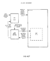
- CS 101's Micro-code Stack Mechanisms 422 on microcode level is effectively comprised of two stack mechanisms.
- the first stack is Micro-instruction Stack (MIS) 424 while the second stack is referred to as Monitor Stack (MOS) 426.
- MIS Micro-instruction Stack
- MOS Monitor Stack
- CS 101 SIN Microcode 428 and MIS 424 are primarily concerned with execution of SOPs of user's programs.
- Monitor Microcode 430 and MOS 426 are concerned with operation of certain CS 101 internal functions.
- Monitor functions may be performed by a separate CPU operating in conjunction with the machine's primary CPU.
- CS 101 a single hardware CPU is used to perform both functions with actual execution of both functions performed by separate groups of microcode.
- Monitor microcode operations may be initiated either by certain SINs 414 or by control signals generated directly by CS 101's Hardware 418. Invocation of Monitor Microcode 430 by Hardware 418 generated signals insures that CS 101's monitor functions may always be invoked.
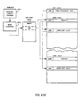
- CS 101's stack mechanisms form single user's program. Our rocedure, is shown. Basically, and with exception of MOS 426, CS 101's stacks reside in MEM 112 with certain portions of those stacks accelerated into FU 120 and EU 122 to enhance speed of operation.
- MEM 112 storage space Certain areas of MEM 112 storage space are set aside to contain Macro-Stacks (MASs) 502, stack mechanisms operating on the SINs level, as described above. Other areas of MEM 112 are set aside to contain Secure Stack (SS) 504, operating on the microcode level, as described above and of which MIS 424 is a part.
- MASs Macro-Stacks
- SS Secure Stack
- both FU 120 and EU 122 contain register file arrays, referred to respectively as GRF and ERF, in addition to registers associated with, for example, ALUs.
- GRF 506 is horizontally divided into three areas.
- a first area referred to as General Registers (GRs) 508 may in general be used in the same manner as registers in a conventional machine.
- a second area of GRF 506 is Micro-Stack (MIS) 424, and is set aside to contain a portion of a Process's SS 504.
- MIS Micro-Stack
- a third portion of GRF 506 is set aside to contain MOS 426.
- mCS Microcode Control State
- mCS 510 represents registers and other FU 120 hardware containing current operating state of FU 120 on the microinstruction and hardware level.
- mCS 510 may include, for example, the current microinstruction controlling operation of FU 120.
- EUS 512 is similar to mCS 510 in FU 120 and includes all registers and other EU 122 hardware containing information reflecting EU 122's current operating state.
- SOP Stack 518 is a portion of EU 122's ERF 516 which has been set aside as a stack mechanism to contain a portion of a process's SS 504 pertaining to EU 122 operations.
- MASs 502 operate generally upon the SINs level.
- MASs 502 are used in general to store current state of a process's (defined below) execution of a user's program.
- MIS 424 in a present embodiment of CS 101 that portion of GRF 506 set aside to contain MIS 424 may have a capacity of eight stack frames. That is, up to 8 microinstruction level interrupts or calls pertaining to execution of a user's program may be stacked within MIS 424.
- Information stored in MIS 424 stack frames is generally information from GR 508 and MCS 510.
- MIS 424 stack frames are transferred between MIS 424 and SS 504 such that at least one frame, and no more than 8 frames, of SS 504 reside in GRF 506.
- SS 504 residing in MEM 112 may contain, for all practical purposes, an unlimited number of frames so that MIS 424 and SS 504 appear to a user to be effectively an infinitely deep stack.
- MOS 426 resides entirely in FU 120 and, in a present embodiment of CS 101, may have a capacity of 8 stack frames.
- a feature of CS 101 operation is that CS 101 mechanisms for handling certain events or interrupts should not rely in its operation upon those portions of CS 101 whose operation has resulted in those faults or interrupts.
- events handled by CS 101 monitor microcode, for example, are MEM 112 page faults.
- An MEM 112 page fault occurs whenever FU 120 makes a reference to data in MEM 112 and that data is not in MEM 112. Due to this and similar operations, MOS 426 resides entirely in FU 120 and thus does not rely upon information in MEM 112.
- GRs 508, MIS 424, and MOS 426 each reside in certain assigned portions of GRF 506. This allows flexibility in modifying the capacity of GRs 508, MIS 424, and MOS 426 as indicated by are required to express a user's program. Also, use of SOPs allows easier and simpler construction of compilers, and facilitates adaption of CS 101 systems to new user languages. In addition, use of Names to refer to operands means that SOPs are independent of the form of the operands upon which they operate. This in turn allows for more compact code in expressing user programs in that SOPs specifying operations dependent upon operand form are not required.
- a user's program residing in CS 101 will include one or more Objects.
- a Procedure Object contains at least the SINs of the user's programs and a Name Table containing entries for operand Names of the program. The SINs may include references, or calls, to other Procedure Objects containing, for example, procedures available in common to many users.
- a Static Data Area may contain static data, that is data having an existence for at least a single execution of the program.
- a Macro-stack described below, may contain local data, that is data generated during execution of a program.
- Each Procedure Object, the Static Data Area and the Macro-stack are individual Objects identified by UIDs and AONs and addressable through UID and AON addresses and descriptors.
- ABPs Architectural Base Pointers
- location information in Name Tables is expressed as offsets from one of the ABPs.
- ABPs may be expressed as previously described.
- the three ABPs are the Frame Pointer (FP), the Procedure Base Pointer (PBP), and the Static Data Pointer (SDP). Locations of data local to a procedure, for example in the procedure's Macrostack, are described as offsets from FP. Locations of non-local data, that is Static Data, are described as offsets from SDP. Locations of SINs in Procedure Objects are expressed as offsets from PBP; these offsets are determined as a Program Counter (PC) value. Values of the ABPs vary during program execution and are therefore not provided by the compiler converting a user's high level language program into a program to be executed in a CS 101 system. When the program is executed, CS 101 provides the proper values for the ABPs. When a program is actually being executed, the ABP's values are stored in FU 120's GRF.
- Pointers are used, for example, to identify the top frame of CS 101's Secure Stack (a microcode level stack described below) or to identify the microcode Dialect currently being used in execute the SINs of a procedure. These pointers are similar to FP, SDP, and PBP.
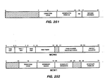
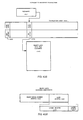
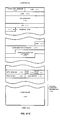
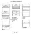
- FIG. 4 and 4A diagramic representations of various control levels and stack mechanisms of, respectively, conventional machines and CS 101, are shown.
- top level of control is provided by User Language Instructions 402, for example in FORTRAN or COBOL.
- User Language Instructions 402 are converted into a greater number of more detailed Machine Language Instructions 404, used within a machine to execute user's programs.
- Machine Language Instructions 404 are interpreted and executed by Microcode Instructions 406, that is sequences of microinstructions which in turn directly control Machine Hardware 408.
- Some conventional machines may include a Stack Mechanism 410 used to save current machine state, that is current microinstruction and contents of various machine registers, if a current Machine Language Instruction 404 cannot be executed or is interrupted. In general, machine state on the microcode and hardware level is not saved. Execution of a current Machine Language Instruction 404 is later resumed at start of the microinstruction sequence for executing that Machine Language Instruction 404.
- top level control in CS 101 is by User Language Instructions 412 as in a conventional machine.
- User Language Instructions 412 are translated into SOPs 414 which are of a higher level than conventional machine language instructions.
- SOPs 414 are interpreted and executed by Microcode Instructions 416 (sequences of microinstructions) which directly control CS 101 Hardware 418.
- CS 101 includes a Macro-stack Mechanism (MAS) 420, at SOPs 414 level, which is comparable to but different in construction and operation from a conventional Machine Language Stack Mechanism 410.
- CS 101 also includes Micro-code Stack Mechanisms 422 operating at Microcode 416 level, so that execution of experience, or to modify an individual CS 101 for particular purposes.
- MAS Macro-stack Mechanism
- EUS 512 is functionally a part of a process's SS 504. Also as previously described, EU 122 performs arithmetic operations in response to SINs and may be interrupted by FU 120 to aid certain FU 120 operations. EUS 512 allows stacking of interrupts. For example, FU 120 may first interrupt an arithmetic SOP to request EU 122 to aid in evaluation of a Name Table Entry. Before that first interrupt is completed, FU 120 may interrupt again, and so on.
- SOP Stack 514 is a single frame stack for storing current state of EU 122 when an interrupt interrupts execution of an arithmetic SOP.
- An interrupted SOP's state is transferred into SOP Stack 514 and the interrupt begins execution in EUS 512.
- EU's first interrupt state is transferred from EUS 512 to a stack frame in SS 504, and execution of the second interrupt begins in EUS 512.
- EU's second interrupt state is transferred from EUS 512 to another stack frame in SS 504 and execution of the third interrupt is begun in EUS 512; and so on.
- EUS 512 and SS 504 thus provide an apparently infinitely deep microstack for EU 122.
- state of second interrupt is transferred from SS 504 to EUS 512 and execution of second interrupt resumed.
- state of first interrupt is transferred from SS 504 to EUS 512 and completed.
- state of the original SOP is transferred from SOP Stack 514 to EUS 512 and execution of that SOP resumed.
- a Procedure 602 includes a User's Procedure Object 604 containing the SOPs of the user's program and a Name Table containing Entries for operand Names of the user's program, and a Static Data Area 606.
- a Procedure 602 may also include other Procedure Objects 608, for example utility programs available in common to many users. In effect, a Procedure 602 contains the instructions (procedures) and data of a user's program.
- a Process 610 includes, as described above, a Macro-Stack (MAS) 502 storing state of execution of a user's Procedure 602 at the SOP level, and a Secure Stack (SS) 504 storing state of execution of a user's Procedure 602 at the microcode level.
- a Process 610 is associated with a user's Procedure 602 through the ABPs described above and which are stored in the MAS 502 of the Process 610.
- the MAS 502 and SS 504 of a Process 610 are associated through non-architectural pointers, described above.
- a Process 602 is effectively a body of information linking the resources, hardware, microcode, and software,.of CS 101 to a user's Procedure 602.
- a Process 610 makes the resources of CS 101 available to a user's Procedure 602 for executing of that Procedure 602.
- CS 101 is a multi-program machine capable of accommodating up to, for example, 128 Processes 610 concurrently.
- the number of Processes 610 which may be executed concurrently is determined by the number of Virtual Processors 612 of CS t01. There may be, for example, up to 16 Virtual Processors 612.
- a Virtual Processor 612 is comprised of a Virtual Processor State Block (VPSB) 614 associated with the SS 504 of a Process 612.
- VPSB 614 is, in effect, a body of information accessible to CS 101's operating system and through which CS 101's operating system is informed of, and provided with access to, a Process 610 through that Process 610's SS 504.
- a VPSB 614 is associated with a particular Process 610 by writing information regarding that Process 610 into that VPSB 614.
- CS 101's operating system may, by gaining access to a Process 610 through an associated PSB 614, read information, such as ABP's, from that Process 610 to FU 120, thereby swapping that Process 610 onto FU 120 for execution. It is said that a Virtual Processor 612 thereby executes a Process 610; a Virtual Processor 612 may be regarded therefor, as a processor having "Virtual", or potential, existence which becomes "real" when its associated Process 610 is swapped into FU 120. In CS 101, as indicated in Fig. 6, only one Virtual Processor 612 may execute on FU 120 at a time and the operating system selects which Virtual Processor 612 will excecute on FU 120 at any given time. In addition, CS 101's operating system selects which Processes 610 will be associated with the available Virtual Processors 612.
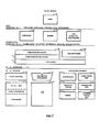
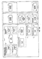
- CS 101 is a multiple level system wherein operations in one level are generally transparent to higher levels.
- User 701 does not see the S-Language, addressing, and protection mechanisms defined at Architectural Level 708. Instead, he sees User Interface 709, which is defined by Compilers 702, Binder 703, and Extended (high level) Operating System (EOS) 704.
- Compilers 702 translate high-level language code into SINs and Binder 703 translates symbolic Names in programs into UID-offset addresses.
- FIG. 7 shows, Architectural Level 708 is not defined by FU 120 Interface 711. Instead, the architectural resources level are created by S-Language interpreted SINs when a program is executed; Name Interpreter 715 operates under control of S-Language Interpreters 705 and translates Names into logical descriptors.
- both S-Language Interpreters 705 and Name Interpreter 715 are implemented as microcode which executes on FU 120. S-Language Interpreters 705 may also use EU 122 to perform calculations.
- a Kernel Operating System (KOS) provides CS 101 with UID-offset addressing, objects, access checking, processes, and virtual processors, described further below.
- KOS Kernel Operating System
- KOS has three kinds of components: KOS Microcode 710, KOS Software 706, and KOS Tables in MEM 112.
- KOS 710 components are microcode routines which assist FU 120 in performing certain required operations.
- KOS 706 components contain SINs which are interpreted by S-Interpreter Microcode 705.
- Many KOS High-Level Language Routines 706 are executed by special KOS processes; others may be executed by any process.
- Both KOS High-Level Language Routines 706 and KOS Microcode 710 manipulate KOS Tables in MEM 112.
- FU 120 Interface 711 is visible only to KOS and to S-Interpreter Microcode 705.
- FU 120 may be seen as a processor which contains the following main elements:
- microcode which executes on FU 120 uses these devices; there is in addition a group of devices for performing special functions; these devices are used only by microcode connected with those functions.
- the microcode, the specialized devices, and sometimes tables in MEM 112 make up logical machines for performing certain functions. These machines will be described in detail below.
- Compilers 702 (Fig. 7)
- Compilers 702 translate files containing the high-level language code written by User 701 into Procedure Objects 608.
- Two components of a Procedure Object 608 are code (SOPs) and Names, previously described. SOPs represent operations, and the Names represent data. A single SIN thus specifies an operation to be performed on the data represented by the Names.
- Binder 703 (Fig. 7)
- Compiler 702 cannot define locations as offsets from an ABP. For example, if a procedure calls a procedure contained in another procedure object, the location to which the call transfers control cannot be defined as an offset from the PBP used by the calling procedure. In these cases, the compiler uses symbolic Names to define the locations. Binder 703 is a utility which translates symbolic Names into UID-offset addresses. It does so in two ways: by combining separate Procedure Objects 608 into a single large Procedure Object 608, and then redefining symbolic Names as offsets from that Procedure Object 608's ABPs, or by translating symbolic Names when the program is executed. In the second case, Binder 703 requires assistance from EOS 704.
- EOS 704 manages the resources that User 701 requires to execute his programs. From User 701's point of view, the most important of these resources are files and processes. EOS 704 creates files by requesting KOS to create an object and then mapping the file onto the object. When a User 701 performs an operation on a file, EOS 704 translates the file operation into an operation on an object. KOS creates them at EOS 704's request and makes them available to EOS 704, which in turn makes them available to User 701. EOS 704 causes a process to execute by associating it a Virtual Processor 612. In logical terms, a Virtual Processor 612 is the means which KOS provides EOS 704 for executing Processes 610.
- Processes 610 may apparently execute simultaneously in CS 101 as there are Virtual Processors 612.
- the illusion of simultaneous execution is created by multiplexing JP 114 among the Virtual Processors; the manner in which Processes 610 and Virtual Processors 610 are implemented will be explained in detail below.
- S-Interpreter Microcode 710 and Name Interpreter Microcode 715 require an environment provided by KOS Microcode 710 and KOS Software 706 to execute SINs.
- KOS Microcode 710 and KOS Software 706 to execute SINs.
- Names and program locations are defined in terms of ABPs whose values vary during execution of the program.
- the KOS environment provides values for the ABP S , and therefore makes it possible to interpret Names and program locations as locations in MEM 112.
- KOS help is required to transform logical descriptors into references to MEM 112 and to perform protection checks.
- KOS The environment provided by KOS has the following elements:
- FIG. 8 gives a high-level view of their physical implementation.
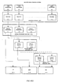
- Fig. 8 illustrates the relationship between Processes 610, Virtual Processors 612, and JP 114.
- a Process 610 is an area of MEM 112 which contains the current state of a user's execution of a program.
- One example of such state is the current values of the ABPs and a Program Counter (PC).
- PC Program Counter
- the next SOP in the program can be executed; similarly, given the current values of SDP and FP, the program's Names can be correctly resolved. Since the Process 610 contains the current state of a program's execution, the program's physical execution can be stopped and resumed at any point. It is thus possible to control program execution by means of the Process 610.
- a Process 610's execution proceeds only when KOS has bound it to a Virtual Processor 612, that is, an area of MEM 112 containing the state required to execute microinstructions on JP 114 hardware.
- the operation of binding is simply a transfer of Process 610 state from the Process 610's area of MEM 112 to a Virtual Processor 612's area of MEM 112. Since binding and unbinding may take place at any time, EOS 704 may multiplex Processes 610 among Virtual Processors 612. In Fig. 8, there are more Processes 610 than there are Virtual Processors 612.
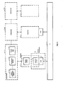
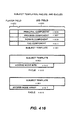
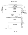
- a Process 610 is made up of six Objects: one Process Object 901 and Five Stack Objects 902 to 906.
- Fig. 9 illustrates a Process 610.
- Process Object 901 contains the information which EOS 704 requires to manage the Process 610.
- EOS 704 has no direct access to Process Object 901, but instead obtains the information it needs by means of functions provided to it by KOS 706, 710. Included in the information are the UIDs of Stack Objects 902 through 906.
- Stack Objects 902 to 906 contain the Process 610's state.
- Stack Objects 902 through 905 are required by CS 101's domain protection method and comprise Process 610's MAS 502.
- a domain is determined in part by operations performed when a system is operating in that domain.
- the system is in EOS 704 domain when executing EOS 704 operations and in KOS 706, 710 domain when executing KOS 706, 710 operations.
- a Process 610 must have one stack for each domain it enters. In the present embodiment, the number of domains is fixed at four, but alternate embodiments may allow any number of domains, and correspondingly, any number of Stack Objects.
- Stack Object 906 comprises Process 610's Secure Stack 504 and is required to store state which may be manipulated only by KOS 706, 710.
- Each invocation made by a Process 610 results in the addition of frames to Secure Stack 504 and to Macro-Stack 502.
- the state stored in the Secure Stack 504 frame includes the macrostate for the invocation, the state required to bind Process 610 to a Virtual Processor 612.
- the frame added to Macro-Stack 502 is placed in one of Stack Objects 902 through 905. Which Stack Objects 902 to 905 gets the frame is determined by the invoked procedure's domain of execution.
- Fig. 9 shows the condition of a Process 610's MAS 502 and Secure Stack 504 after the Process 610 has executed four invocations.
- Secure Stack 504 has one frame for each invocation; the frames of Process 610's MAS 502 are found in Stack Objects 902, 904, and 905.
- Frame 1 is for an invocation of a routine with KOS 706, 710 domain of execution
- Frame 2 for an invocation of a routine with the EOS 704 domain of execution
- Frames 3 and 4 for invocations of routines with the User domain of execution.
- Process 610 has not yet invoked a routine with the Data Base Management System (DBMS) domain of execution.
- DBMS Data Base Management System
- the frames in Stack Objects 902 through 905 are linked together, and a frame is added to or removed from Secure Stack 504 every time a frame is added to Stack Objects 902 through 905.
- MAS 502 and Secure Stack 504 thereby function as a single logical stack even though logically contained in five separate Objects.
- KOS 706, 710 performs a call for a process, it does the following:
- the PC is defined, Names can be resolved, and execution of the invoked routine can commence.
- the stack frames are deleted and the ABPs are set to the values saved in the invoking routine's macrostate.
- the invoking routine then continues execution at the point following the invocation.
- a Process 610 may be illustrated in detail by putting the FORTRAN statement A + B into a FORTRAN routine called EXAMPLE and invoking it from another FORTRAN routine named CALLER.
- EXAMPLE a FORTRAN routine
- CALLER and EXAMPLE both have the same domain of execution.
- the parts of EXAMPLE which are of interest look like this:
- the new elements are a formal argument.
- C and a new local variable, X.
- a formal argument is a data item which receives its value from a data item used in the invoking routine. The formal argument's value thus varies from invocation to invocation.
- the portions of INVOKER which are of interest look like this:
- the CALL statement in INVOKER specifies the Name of the subroutine being invoked and the actual arguments for the subroutine's formal arguments. During the invocation, the subroutine's formal arguments take on the values of the actual arguments. Thus, during the invocation specified by this CALL statement, the formal argument C will have the value represented by the variable Z in INVOKER.
- the compiler When INVOKER is compiled, the compiler produces a CALL SIN corresponding to the CALL statement.
- the CALL SIN contains a Name representing a pointer to the beginning of the called routine's location in a procedure object and a list of Names representing the call's actual arguments.
- the Names are interpreted to resolve the SIN's Names as previously described, and KOS 710 microcode to perform MAS 502 and Secure Stack 504 operations.
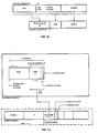
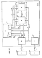
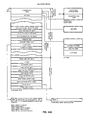
- Fig. 10 illustrates the manner in which the KOS 710 call microcode manipulates MAS 502 and Secure Stack 504.
- Fig. 10 includes the following elements:
- KOS Call Microcode 1001 first saves the macrostate of INVOKER's invocation on Secure Stack 504. As will be discussed later, when the state is saved, KOS 706 Call Microcode 1001 uses other KOS 706 microcode to translate the location information contained in the macrostate into the kind of pointers used in MEM 112. Then Microcode 1001 uses the descriptor for the routine Name to locate the pointer to EXAMPLE' S entry in Procedure Object 1006. From the entry, it locates pointers to EXAMPLE' S Name Table and the beginning of EXAMPLE' S code.
- Microcode 1001 takes these pointers, uses other KOS 706 microcode to translate them into descriptors, and places the descriptors in the locations in Registers 1004 reserved for the values of the PBP and NTP. It then updates the values contained in PC Device 1002 so that when the call is finished, the next SIN to be executed will be the first SIN in EXAMPLE.
- CALL Microcode 1001 next constructs the frames for EXAMPLE on Secure Stack 504 and Macro-Stack 502. This discussion concerns itself only with Frame 1102 on Macro-Stack 502.
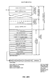
- Fig. 11 illustrates EXAMPLE' S Frame 1102.
- the size of Frame 1102 is determined by EXAMPLE' S local variables (X, A, and B) and formal arguments (C).
- Header 1104. contains information used by KOS 706, 710 to manage the stack.
- Pointer 1106 to the location which contains the value represented by the argument C.
- the actual for C is the local variable Z in INVOKER.
- the storage represented by Z is contained in the stack frame belonging to INVOKER's invocation.
- a name interpreter resolved C's name, it placed the descriptor in a register.
- Call Microcode 1001 takes this descriptor, converts it to a pointer, and stores the pointer above Header 1104.
- EXAMPLE' S Procedure Object 1006 contains the size of the storage required for the local variables, so Call Microcode 1001 obtains this information from Procedure Object 1006 and adds that much storage to Frame 1102.
- Name Interpreter 715 can now construct descriptors for the local data. For example, A's entry in Name Table specified that it was offset 32 bits from FP, and was 32 bits long. Thus, its storage falls between the storage for X and B in Figure 11.
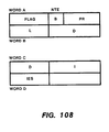
- a logical descriptor contains an AON field, an offset field, and a length field.
- Fig. 12 illustrates a Physical Descriptor.
- Physical Descriptor 1202 contains a Frame Number (FN) field, a Displacement (D) field, and a Length (L) field. Together, the Frame Number field and the Displacement field specify the location in MEM 112 containing the data, and the Length field specifies the length of the data.
- FN Frame Number
- D Displacement
- L Length
- the virtual memory management system must translate the AON-offset location contained in a logical descriptor 1204 into a Frame Number-Displacement location. It does so by associating logical pages with MEM 112 frames. (N.B: MEM 112 frames are not to be confused with stack frames).
- Fig.13 illustrates how Macrostack 502 Object 1302 is divided into Logical Pages 1304 in secondary memory and how Logical Pages 1304 are moved onto Frames 1306 in MEM 112.
- a Frame 1306 is a fixed-size, contiguous area of MEM 112. When the virtual memory management system brings data into MEM 112, it does so in frame-sized chunks called Logical Pages 1308.
- each object is divided into Logical Pages 1308 and the address of data on a page consists of the AON of the data's Object, the number of pages in the object, and its displacement on the page.
- the location of the local variable B of EXAMPLE is shown as it is defined by the virtual memory system.
- B's location is a UID and an offset, or, inside JP 114, an AON and an offset.
- B's location is the AON, the page number 1308, and a displacement within the page.
- the virtual memory management system must therefore perform two kinds of translations: (1) AON-offset addresses into AON-page number-displacement addresses, and (2) AON-page number into a frame number.
- KOS 706, 710 checks whether the reference is legal. The following discusson will first present the logical structure of access control in CS 101, and then discuss the microcode and devices which implement it.
- CS 101 defines access in terms of subjects, modes of access, and Object size.
- a process may reference a data item located in an Object if three conditions hold:
- ACL Access Control List
- An Object's size is one of its attributes. Neither an Object's size nor its ACL is contained in the Object. Both are contained in system tables, and are accessible by means of the Object's UID.
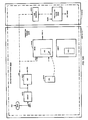
- Fig. 14 shows the logical structure of access control in CS 101.
- Subject 1408 has four components: Principal ocess 1405, Domain 1406, and Tag 1407.
- Tag 1407 is not implemented in a present embodiment of CS 101, so the following description will deal only with Principal 1404, Process 1405, and Domain 1406.
- Each component of the Subject 1408 is represented by a UID. If the UID is a null UID, that component of the subject does not affect access checking.
- Non-null UIDs are the UIDs of Objects that contain information about the subject components.
- Principal Object 1404 contains identification and accounting information regarding system users
- Process Object 1405 contains process management information
- Domain Object 1406 contains information about per-domain error handlers.
- Read and write are self-explanatory; execute is access which allows a subject to execute instructions contained in the Object.
- Access Control Lists are made up of Entries 1414. Each entry two components: Subject Template 1416 and Mode Specifier 1418.
- Subject Template 1416 specifies a group of subjects that may reference the Object and Mode Specifier 1418 specifies the kinds of access these subjects may have to the Object.
- ACL 1412 is checked each time a process references an Object 1410. The reference may succeed only if the process's current Subject 1408 is one of those on Object 1410's ACL 1412 and if the modes in the ACL Entry 1414 for the Subject 1408 allow the kind of access the process wishes to make.
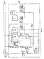
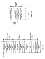
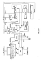
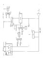
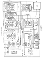
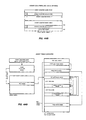
- Fig. 15 illustrates the devices and tables which KOS 706, 710 uses to implement Virtual Processors 612.
- FU 120 WCS contains KOS Microcode 706 for binding Virtual Processors 612 to JP 114 and removing them from JP 114.
- Timers 1502 and Interrupt Line 1504 are hardware devices which produce signals that cause the invocation of KOS Microcode 706.
- Timers 1502 contains two timing devices: Interval Timer 1506, which may be set by KOS 706, 710 to signal when a certain time is reached, and Egg Timer 1508, which guarantees that there is a maximum time interval for which a Virtual Processor 612 can be bound to JP 114 before it invokes KOS Microcode 706.
- Interrupt Line 1504 becomes active when JP 114 receives a message from IOS 116, for example when IOS 116 has finished loading a logical page into MEM 112.
- Registers 508 contain state belonging to the Virtual Processor 612 currently bound to JP 114.
- this Virtual Processor 612 is called Virtual Processor A.
- Registers 508 contain registers reserved for the execution of VP Swapping Microcode 1510.
- ALU 1942 (part of FU 120) is used for the descriptor-to-pointer and pointer-to-descriptor transformations required when one Virtual Processor 612 is unbound from JP 114 and another bound to JP 114.
- MEM 112 contains data bases for Virtual Processors 612 and data bases used by KOS 706, 710 to manage Virtual Processors 612.
- KOS 706, 710 provides a fixed nurpber of Virtual Processors 612 for CS 101.
- Each Virtual Processor 612 is represented by a Virtual Processor State Block (VPSB) 614.
- Each VPSB 614 contains information used by KOS 706, 710 to manage the Virtual Processor 612, and in addition contains information associating the Virtual Processor 612 with a process.
- Fig. 15 shows two VPSBs 614, one belonging to Virtual Processor 612A, and another belonging to Virtual Processor 612B, which will replace Virtual Processor 612A on JP 114.
- the VPSBs 614 are contained in VPSB Array 1512.
- the index of a VPSB 614 in VPSB Array 1512 is Virtual Processor Number 1514 belonging to the Virtual Processor 612 represented by a VPSB 614.
- Virtual Processor Lists 1516 are lists which KOS 706, 710 uses to manage Virtual Processors 612. If a Virtual Processor 612 is able to execute, its Virtual Processor Number 1514 is on a list called the Runnable List; Virtual Processors 612 which cannot run are on other lists, depending on the reason why they cannot run. It is assumed that Virtual Processor 612B's Virtual Processor Number 1514 is the first one on the Runnable List.
- the Virtual Processor Number 1514 is copied into the process's Process Object 901 and the AONs of the process's Process Object 901 and stacks are copied into the Virtual Processor 612's VPSB 614.
- AONs are used because a process's stacks are wired active as long as the process is bound to a Virtual Processor 612).
- Binding is carried out by KOS 706, 710 at the request of EOS 704.
- two Secure Stack Objects 906 are shown, one belonging to the process to which Virtual Processor 612A is bound, and one belonging to that to which Virtual Processor 612B is bound.
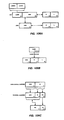
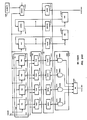
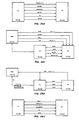
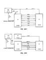
- IOS 116 (Figs. 16, 17
- IOS 116 a partial block diagram of IOS 116 is shown.
- IOS 116 include an ECLIPSE® Burst Multiplexer Channel (BMC) 1614 and a NOVA® Data Channel (NDC) 1616, an 10 Controller (IOC) 1618 and a Data Mover (DM) 1610.
- IOS 116's data channel devices for example BMC 1914 and NDC 1616, comprise IOS 116's interface to the outside world.
- Information and addresses are received from external devices, such as disk drives, communications modes, or other computer systems, by IOS 116's data channel devices and are transferred to DM 1610 (described below) to be written into MEM 112.
- DM 1610 described below
- information read from MEM 112 is provided through DM 1610 to IOS 116's data channel devices and thus to the above described external devices.
- These external devices are a part of CS 101's addressable memory space and may be addressed through UID addresses.
- IOC 1618 is a general purpose CPU, for example an ECLIPSE® computer available from Data General Corporation. A primary function of IOC 1618 is control of data transfer through IOS 116. In addition, IOC 1618 generates individual Maps for each data channel device for translating external device addresses into physical addresses within MEM 112. As indicated in Fig. 16, each data channel device contains an individual Address Translation Map (MAP) 1632 and 1636. This allows IOS 116 to assign individual areas of MEM 112's physical address space to each data channel device. This feature provides protection against one data channel device writing into or reading from information belonging to another data channel device. In addition, IOC 1618 may generate overlapping address translation Maps for two or more data channel devices to allow these data channel devices to share a common area of MEM 112 physical address space.
- MAP Address Translation Map
- DM 1610 Data transfer between IOS 116's data channel devices and MEM 112 is through DM 1610, which includes a Buffer memory (BUF) 1641. BUF 1641 allows MEM 112 and IOS 116 to operate asychronously. DM 1610 also includes a Ring Grant Generator (RGG) 1644 which controls access of various data channel devices to MEM 112. RGG 1644 is designed to be flexible in apportioning access to MEM 112 among IOS 116's data channel devices as loads carried by various data channel devices varies. In addition, RGG 1644 insures that no one, or group, of data channel devices may monopolize access to MEM 112.
- RGG Ring Grant Generator
- RGG 1644 may be regarded as a commutator scanning a number of ports which are assigned to various channel devices. For example, ports A, C, E, and G may be assigned to a BMC 1614, ports B and F to a NDC 1616, and ports D and H to another data channel device. RGG 1644 will scan each of these ports in turn and, if the data channel device associated with a particular port is requesting access to MEM 112, will grant access to MEM 112 to that data channel device. If no request is present at a given port, RGG 1644 will continue immediately to the next port.
- Each data channel device assigned one or more ports is thereby insured opportunity of access to MEM 112.
- Unused ports for example indicating data channel devices which are not presently engaged in information transfer, are effectively skipped over so that access to MEM 112 is dynamically modified according to the information transfer loads of the various data channel devices.
- RGG 1644's ports may be reassigned among IOS 116's various data channel devices as required to suit the needs of a particular CS 101 system. If, for example, a particular CS 101 utilizes NDC 1616 more than a BMC 1614, that CS 101's NDC 1616 may be assigned more ports while that CS 101's BMC 1614 is assigned fewer ports.
- Memory (MEM) 112 (Fi g , 18)
- MEM 112 a partial block diagram of MEM 112 is shown.
- Major elements of MEM 112 are Main Store Bank (MSB) 1810, a Bank Controller (BC) 1814, a Memory Cache (MC) 1816, a Field Interface Unit (FIU) 1820, and Memory Interface Controller (MIC) 1822. Interconnections of these elements with input and output buses of MEM 112 to IOS 116 and JP 114 are indicated.
- MSB Main Store Bank
- BC Bank Controller
- MC Memory Cache
- FU Field Interface Unit
- MIC Memory Interface Controller
- MEM 112 is an intelligent, prioritizing memory having a single port to IOS 116, comprised of IOM Bus 130, MIO Bus 129, and IOMC Bus 131, and dual ports to JP 114.
- a first JP 114 port is comprised of MOD Bus 140 and PD Bus 146, and a second port is comprised of JPD Bus 142 and PD Bus 146.
- all data transfers from and to MEM 112 by IOS 116 and JP 114 are of single, 32 bit words; IOM Bus 130, MIO Bus 129, MOD Bus 140, and JPD Bus 142 are each 32 bits wide.
- CS 101 is a variable word length machine wherein the actual physical width of data buses are not apparent to a user.
- a Name in a user's program may refer to an operand containing 97 bits of data.
- that 97 bit data item will appear to be read from MEM 112 to JP 114 in a single operation.
- JP 114 will read that operand from MEM 112 in a series of read operations referred to as a string transfer.
- the string transfer will comprise three 32 bit read transfers and one single bit read transfer.
- the final single bit transfer, containing a single data bit will be of a 32 bit word wherein one bit is data and 31 bits are fill.
- Write operations to MEM 112 may be performed in the same manner.
- a single read or write request to MEM 112 specifies a data item of less than 32 bits of data, that transfer will be accomplished in the same manner as the final transfer described above. That is, a single 32 bit word will be transferred wherein non-data bits are fill bits.
- MSB 1810 Bulk data storage in MEM 112 is provided in MSB 1810, which is comprised of one or more Memory Array cards (MAs) 1812.
- MAs Memory Array cards
- BC 1814 performs all control and timing functions for MAs 1812.
- BC 1814's functions include addressing, transfer of data, controlling whether a read or write operation is performed, refresh, sniffing, and error correction code operations. All read and write operations from and to MAs 1812 through BC 1814 are in blocks of four 32 bit words.
- the various MAs 1812 comprising MSB 1810 need not be of the same data storage capacity. For example, certain MAs 1812 may have a capacity of 256 kilobytes while other MAs 1812 may have a capacity of 512 kilobytes. Addressing of the MAs 1812 in MSB.1810 is automatically adapted to various MA 1812 configurations. As indicated in Fig. 18, each MA 1812 contains an address circuit (A) which receives an input from the next lower MA 1812 indicating the highest address in that next lower MA 1812. The A circuit on an MA 1812 also receives an input from that MA 1812 indicating the total address space of that MA 1812.
- A address circuit
- the A circuit of that MA 1812 adds the highest address input from next lower MA 1812 to its own input representing its own capacity and generates an output to the next MA 1812 indicating its own highest address. All MAs 1812 of MSB 1810 are addressed in parallel by BC 1814. Each MA 1812 compares such addresses to its input from the next lower MA 1812, representing highest address of that next lower MA 1812, and its own output, representing its own highest address, to determine whether a particular address provided by BC 1814 lies within the range of addresses contained within that particular MA 1812. The particular MA 1812 whose address space includes that address will then respond by accepting the read or write request from BC 1814.
- MC 1816 is the data path for transfer of data between BC 1814 and IOS 116 and JP 114.
- MC 1816 contains a high speed cache storing data from MSB 1810 which is currently being utilized by either IOS 116 or JP 114.
- MSB 1810 thereby provides MEM 112 with a large storage capacity while MC 1816 provides the appearance of a high speed memory.
- MC 1816 includes a bypass write path which allows IOS 116 to write blocks of four 32 bit words directly into MSB 1810 through BC 1814.
- MC 1816 includes a cache write-back path which allows data to be transferred out of MC 1816's cache and stored while further data is transferred into MC 1816's cache.
- Displaced data from MC 1816's cache may then be written back into MSB 1810 at a later, more convenient time.
- This write-back path enhances speed of operation of MC 1816 by avoiding delays incurred by transferring data from MC 1816 to MSB 1810 before new data may be written into MC 1816.
- MEM 112's FIU 1820 allows manipulation of data formats in writes to and reads from MEM 112 by both JP 114 and IOS 116. For example, FIU 1820 may convert unpacked decimal data to packed decimal data, and vice versa. In addition, FIU 1820 allows MEM 112 to operate as a bit addressable memory. For example, as described all data transfers to and from MEM 112 are of 32 bit words. If a data transfer of less than 32 bits is required, the 32 bit word containing those data bits may be read from MC 1816 to FIU 1820 and therein manipulated to extract the required data bits.
- FIU 1820 then generates a 32 bit word containing those required data bits, plus fill bits, and provides that new 32 bit word to JP 114 or IOS 116.
- data is transferred onto IOM Bus 130, read into FIU 1820, operated upon, transferred onto MOD Bus 140, and transferred from MOD Bus 140 to MC 1816.
- data is transferred from MC 1816 to MOD Bus 140, written into FIU 1820 and operated upon, and transferred onto MIO Bus 129 to IOS 116.
- data is transferred from MC 1816 onto MOD Bus 140, transferred into FIU 1820 and operated upon, and transferred again onto MOD Bus 140 to JP 114.
- data on JPD Bus 142 is transferred into FIU 1820 and operated upon, and is then transferred onto MOD Bus 140 to MC 1816.
- MOD Bus 140 is thereby utilized as an MEM 112 internal bus for FIU 1820 operations.
- MIC 1822 provides primary control of BC 1814, MC 1816, and FIU 1820.
- MIC 1822 receives control inputs from and provides control outputs to PD Bus 146 and IOMC Bus 131.
- MIC 1822 contains primary microcode control for MEM 112, but BC 1814, MC 1816, and FIU 1820 each include internal microcode control.
- Independent, internal microcode controls allow BC 1814, MC 1816, and FIU 1820 to operate independently of MIC 1822 after their operations have been initiated by MIC 1822. This allows BC 1814 and MSB 1810, MC 1816, and FIU 1820 to operate independently and asynchronously. Efficiency and speed of operation of MEM 112 are thereby enhanced by allowing pipelining of MEM 112 operations.
- a primary function of FU 120 is to execute SINs. In doing so, FU 120 fetches instructions and data (SOPs and Names) from MEM 112, returns results of operations to MEM 112, directs operation of FU 122, executes instructions of user's programs, and performs the various functions of CS 101's operating systems. As part of these functions, FU 120 generates and manipulates logical addresses and descriptors and is capable of operating as a general purpose CPU.
- DESP 1910 includes General Register File (GRF) 506.
- GRF 506 is a large register array divided vertically into three parts which are addressed in parallel. A first part, AONGRF 1932 , stores AON fields of logical addresses and descriptors. A second part, OFFGRF 1934, stores offset fields of logical addresses and descriptors and is utilized as a 32 bit wide general register array. A third portion GRF 506, LENGRF 1936, is a 32 bit wide register array for storing length fields of logical descriptors and as a general register for storing data.
- OFFGRF 1934 Primary data path from MEM 112 to FU 120 is through MOD Bus 140, which provides inputs to OFFGRF 1934. As indicated in Fig. 19, data may be transferred from OFFGRF 1934 to inputs of AONGRF 1932 and LENGRF 1936 through various interconnections. Similarly, outputs from LENGRF 1936 and AONGRF 1932 may be transferred to inputs of AONGRF 1932, OFFGRF 1934, and LENGRF 1936.
- Output of OFFGRF 1934 is connected to inputs of DESP 1910's Arithmetic and Logic Unit (ALU) 1942.
- ALU 1942 is a general purpose 32 bit ALU which may be used in generating and manipulating logical addresses and descriptors, as distinct from general purpose arithmetic and logic operands performed by MUX 1940.
- Output of ALU 1942 is connected to JPD Bus 142 to allow results of arithmetic and logic operations to be transferred to MEM 112 or EU 122.
- MUX 1940 Also connected from output of OFFGRF 1934 is Descriptor Multiplexer (MUX) 1940.
- An output of MUX 1940 is provided to an input of ALU 1942.
- MUX 1940 is a 32 bit ALU, including an accumulator, for data manipulation operations.
- MUX 1940, together with ALU 1942, allows DESP 1910 to perform 32 bit arithmetic and logic operations.
- MUX 1940 and ALU 1942 may allow arithmetic and logic operations upon operands of greater than 32 bits by performing successive operations upon successive 32 bit words of larger operands.
- Logical descriptors or addresses generated or provided by DESP 1910 are provided to Logical Descriptor (LD) Bus 1902.
- LD Bus 1902 in turn is connected to an input of Address Translation Unit (ATU) 1928.
- ATU 1928 is a cache mechanism for converting logical descriptors to MEM 112 physical descriptors.
- NC 1926 is a cache mechanism for storing logical descriptors corresponding to operand Names currently being used in user's programs.
- Name Table Entries corresponding to operands currently being used in user's programs are stored in MEM 112.
- Certain Name Table Entries for operands of a user's program currently being executed are transferred from those Name Tables in MEM 112 to FU 120 and are therein evaluated to generate corresponding logical descriptors. These logical descriptors are then stored in NC 1926.
- the instruction stream of a user's program is provided to FU 120's Instruction Buffer (IB) 1962 through MOD Bus 140.
- FU 120's Parser (P) 1964 separates out, or parses, Names from IB 1962 and provides those Names as address inputs to NC 1924.
- NC 1924 in turn provides logical descriptor outputs to LD Bus 1902, and thus to input of ATU 1928.
- NC 1926 input from LD Bus 1902 allows logical descriptors resulting from evaluation of Name Table Entries to be written into NC 1926.
- FU 120's Protections Cache (PC) 1934 is a cache mechanism having an input connected from LD Bus 1902 and providing information, as described further below, regarding protection aspects of references to data in MEM 112 by user's programs.
- NC 1926, ATU 1928, and PC 1934 are thereby acceleration mechanisms of, respectively, CS 101's Namespace addressing, logical to physical address structure, and protection mechanism.
- DESP 1910 includes BIAS 1952, connected from output of LENGRF 1936.
- operands containing more than 32 data bits are transferred between MEM 112 and JP 114 by means of string transfers.
- FU 120 In order to perform string transfers, it is necessary for FU 120 to generate a corresponding succession of logical descriptors wherein length fields of those logical descriptors is no greater than 5 bits, that is, specify lengths of no greater than 32 data bits.
- a logical descriptor describing a data item to be transferred by means of a string transfer will be stored in GRF 506.
- AON field of the logical descriptor will reside in AONGRF 1932, 0 field in OFFGRF 1934, and L field in LENGRF 1936.
- 0 field of that original logical descriptor will be incremented by the number of data bits transferred while L field will be accordingly decremented.
- the logical descriptor residing in GRF 506 will thereby describe, upon each successive transfer of the string transfer, that portion of the data item yet to be transferred.
- 0 field in OFFGRF 1934 will indicate increasingly larger offsets into that data item, while L field will indicate successively shorter lengths.
- AON and 0 fields of the logical descriptor in GRF 506 may be utilized directly as AON and 0 fields of the successive logical descriptors of the string transfer.
- L field of the logical descriptor residing in LENGRF 1936 may not be so used as L fields of the successive string transfer logical descriptors as this L field indicates remaining length of data item yet to be transferred.
- BIAS 1952 generates the 5 bit L fields of successive string transfer logical descriptors while correspondingly decrementing L field of the logical descriptor in LENGRF 1936. During each transfer, BIAS 1952 generates L field of the next string transfer logical descriptor while concurrently providing L field of the current string transfer logical descriptor.
- BIAS 1952 thereby increases speed of execution of string transfers by performing pipelined L field operations.
- BIAS 1952 thereby allows CS 101 to appear to the user to be a variable word length machine by automatically performing string transfers. This mechanism is used for transfer of any data item greater than 32 bits, for example double precision floating point numbers.
- FU 120 includes microcode circuitry for controlling all FU 120 operations described above.
- FU 120 includes a microinstruction sequence control store (mC) 1920 storing sequences of microinstructions for controlling step by step execution of all FU 120 operations.
- mC microinstruction sequence control store
- these FU 120 operations fall into two classes.
- a first class includes those microinstruction sequences directly concerned with executing the SOPs of user's programs.
- the second class includes microinstruction sequences concerned with CS 101's operating systems, including and certain automatic, internal FU 120 functions such as evaluation of Name Table Entries.
- CS 101 is a multiple S-Language machine.
- mC 1920 may contain microinstruction sequences for executing user's SOPs in at least four different Dialects.
- mC 1920 is comprised of a writeable control store and sets of microinstruction sequences for various Dialects may be transferred into and out of mC 1920 as required for execution of various user's programs.
- sets of microinstruction sequences for more than one Dialect in mC 1920 it is possible for user's programs to be written in a mixture of user languages. For example, a particular user's program may be written primarily in FORTRAN but may call certain COBOL routines. These COBOL routines will be correspondingly translated into COBOL dialect SOPs and executed by COBOL microinstruction sequences stored in mC 1920.
- the instruction stream provided to FU 120 from MEM 112 has been previously described with reference to Fig. 3.
- SOPs and Names of this instruction stream are transferred from MOD Bus 140 into IB 1962 as they are provided from MEM 112.
- IB 1962 includes two 32 bit (one word) registers.
- IB 1962 also includes prefetch circuitry for reading for SOPs and Names of the instruction stream from MEM 112 in such a manner that IB 1962 shall always contain at least one SOPs or Name.
- FU 120 includes (P) 1964 which reads and separates, or parses, SOPs and Names from IB 1962.
- P 1964 provides those Names to NC 1926, which accordingly provides logical descriptors to ATU 1928 so as to read the corresponding operands from MEM 112.
- SOPs parsed by P 1964 are provided as inputs to Fetch Unit Dispatch Table (FUDT) 1904 and Execute Unit Dispatch Table (EUDT) 1966.
- FUDT 1904 is effectively a table for translating SOPs to starting addresses in mC 1912 of corresponding microinstruction sequences.
- This intermediate translation of SOPs to mC 1912 addresses allows efficient packing of microinstruction sequences within mC 1912. That is, certain microinstruction sequences may be common to two or more S-Language Dialects. Such microinstruction sequences may therefore be written into mC 1912 once and may be referred to by different SOPs of different S-Language Dialects.
- EUDT 1966 performs a similar function with respect to EU 122.
- EU 122 contains a mC, similar to mC 1912, which is addressed through EUDT 1966 by SOPs specifying EU 122 operations.
- FU 120 may provide such addresses mC 1912 to initiate EU 122 operations as required to assist certain FU 120 operations. Examples of such operations which may be requested by FU 120 include calculations required in evaluating Name Table Entries to provide logical descriptors to be loaded into NC 1926.
- D registers 1905 and 1967 Associated with both FUDT 1904 and EUDT 1966 are Dialect (D) registers 1905 and 1967.
- D registers 1905 and 1967 store information indicating the particular S-Language Dialect currently being utilized in execution of a user's program.
- Outputs of D registers 1905 and 1967 are utilized as part of the address inputs to mC 1912 and EU 122's mC.
- EU 122 is an arithmetic and logic unit provided to relieve FU 120 of certain arithmetic operations. EU 122 is capable of performing addition, subtraction, multiplication, and division operations on integer, packed and unpacked decimal, and single and double precision floating operands. EU 122 is an independently operating microcode controlled machine including Microcode Control (mC) 2010 which, as described above, is addressed by EUDT 1966 to initiate EU 122 operations. mC 2010 also includes logic for handling mutual interrupts between FU 120 and EU 122. That is, FU 120 may interrupt current EU 122 operations to call upon EU 122 to assist an FU 120 operation.
- mC Microcode Control
- FU 120 may interrupt an arithmetic operation currently being executed by EU 122 to call upon EU 122 to assist in generating a logical descriptor from a Name Table Entry.
- EU 122 may interrupt current FU 120 operations when EU 122 requires FU 120 assistance in executing a current arithmetic operation.
- EU 122 may interrupt a current FU 120 operation if EU 122 receives an instruction and operands requiring EU 122 to perform a divide by zero.
- EU 122 includes two arithmetic and logic units.
- a first arithmetic and logic unit (MULT) 2014 is utilized to perform addition, subtraction, multiplication, and division operations upon integer and decimal operands, and upon mantissa fields of single and double precision floating point operands.
- Second ALU (EXP) 2016 is utilized to perform operations upon single and double precision floating point operand exponent fields in parallel with operations performed upon floating point mantissa fields by MULT 2014.
- Both MULT 2014 and EXP 2016 include an arithmetic and logic unit, respectively MALU 2074 and EXPALU 2084.
- MULT 2014 and EXP 2016 also include register files, respectively MRF 2050 and ERF 2080, which operate and are addressed in parallel in a manner similar to AONGRF 1932, OFFGRF 1984 and LENGRF 1936.
- Operands for EU 122 to operate upon are provided from MEM 112 through MOD Bus 140 and are transferred into Operand Buffer (OPB) 2022.
- OPB 2022 performs certain data format manipulation operations to transform input operands into formats most efficiently operated with by EU 122.
- EU 122 and MULT 2014 may be designed to operate efficiently with packed decimal operands.
- OPB 2022 may transform unpacked decimal operands into packed decimal operands. Unpacked decimal operands are in the form of ASCII characters wherein four bits of each characters are binary codes specifying a decimal value between zero and nine. Other bits of each character are referred to as zone fields and in general contain information identifying particular ASCII characters.
- zone field bits may specify whether a particular ASCII character is a number, a letter, or punctuation.
- Packed decimal operands are comprised of a series of four bit fields wherein each field contains a binary number specifying a decimal value of between zero and nine.
- OPB 2022 converts unpacked decimal to packed decimal operands by extracting zone field bits and packing the four numeric value bits of each character into the four bit fields of a packed decimal number.
- EU 122 is also capable of transforming the results of arithmetic operands, for example in packed decimal format, into unpacked decimal format for transfer back to MEM 112 or FU 120.
- a packed decimal result appearing at output of MALU 2074 is written into MRF 2050 through a multiplexer, not shown in Fig. 20, which transforms the four bit numeric code fields of the packed decimal results into corresponding bits of unpacked decimal operand characters, and forces blanks into the zone field bits of those unpacked decimal characters.
- the results of this operation are then read from MRF 2050 to MALU 2074 and zone field bits for those unpacked decimal characters are read from Constant Store (CST) 2060 to MALU 2074.
- CST Constant Store
- MALU 2074 operating under direction of FPC 2002, accordingly right or left shifts one operand's mantissa field to effectively align that operand's exponent field with the other operand's exponent field. Addition or subtraction of the operand's mantissa fields may then proceed.
- EXPALU 2034 also performs addition or subtraction of floating point operand exponent fields in multiplication or division operations, while MALU 2074 performs multiplication and division of the operand mantissa fields. Multiplication and division of floating point operand mantissa fields by MALU 2074 is performed by successive shifting of one operand, corresponding generation of partial products of the other operand, and successive addition and subtraction of those partial products.
- EU 122 performs normalization-of the results of floating point operand operations by left shifting of a final result's mantissa field to eliminate zeros in the most significant characters of the final result mantissa field, and corresponding shifting of the final result exponent fields. Normalization of floating point operation results is controlled by FPC 2002.
- FPC 2002 examines an unnormalized floating point result output of MALU 2074 to detect which, if any, of the most significant characters of that results contain zeros.
- FPC 2002 then accordingly provides control outputs to EXPALU 2034 and MALU 2074 to correspondingly shift the exponent and mantissa fields of those results so as to eliminate leading character zeros from the mantissa field. Normalized mantissa and exponent fields of floating point results may then be transferred from MALU 2074 and EXPALU 2034 to JPD Bus 142 through OM 2024.
- EU 122 also performs addition, subtraction, multiplication, and division operations on operands.
- EU 122 uses a leading zero detector in FPC 2002 in efficiently performing multiplication and division operations.
- FPC 2002's leading zero detector examines the characters or bits of two operands to be multiplied or divided, starting from the highest, to determine which, if any, contain zeros so as not to require a multiplication or division operation.
- FPC 2002 accordingly left shifts the operands to effectively eliminate those characters or bits, thus reducing the number of operations to multiply or divide the operands and accordingly reducing the time required to operate upon the operands.
- EU 122 utilizes a unique method, with associated hardware, for performing arithmetic operations on decimal operands by utilizing circuitry which is otherwise conventionally used only to perform operations upon floating point operands.
- MULT 2074 is designed to operate with packed decimal operands, that is operands in the form of consecutive blocks of four bits wherein each block of four bits contains a binary code representing numeric values of between zero and nine.
- Floating point operands are similarly in the form of consecutive blocks of four bits.
- Each block of four bits in a floating point operand contains a binary number representing a hexadecimal value of between zero and fifteen.
- those operands are loaded, one at a time, into MALU 2074 and, with each such operand, a number comprised of all hexadecimal sixes is loaded into MALU 2074 from CST 2060.
- This CST 2060 number is added to each packed decimal operand to effectively convert those packed decimal operands into hexadecimal operands wherein the four bit blocks contain numeric values in the range of six to fifteen, rather than in the original range of zero to nine.
- MULT 2014 then performs arithmetic operation upon those transformed operands, and in doing so detects and saves information regarding which four bit characters of those operands have resulted in generation of carries during the arithmetic operations.
- the intermediate result resulting from completion of those arithmetic operations upon those transformed operands are reconverted to packed decimal format by subtraction of hexadecimal sixes from those characters for which carries have been generated.
- - EU 122 converts packed decimal operands into "Excess Six" operands, performs arithmetic operations upon those "Excess Six” operands, and reconverts "Excess Six" results of those operations back into packed decimal format.
- FU 120 controls transfer of arithmetic results from EU 122 to MEM 112. In doing so, FU 120 generates a logical descriptor describing the size of MEM 112 address space, or "container", that result is to be transferred into. In certain arithmetic operations, for example integer operations, an arithmetic result may be larger than anticipated and may contain more bits than the MEM 112 "container”.
- Container Size Check Circuit (CSC) 2052 compares actual size of arithmetic results and L fields of MEM 112 "container" logical descriptors. CSC 2052 generates an output indicating whether an MEM 112 "container" is smaller than an arithmetic result.
- CSC Container Size Check Circuit
- CS 10110 a partial block diagram of Computer System (CS) 10110 is shown.
- Major elements of CS 10110 are Dual Port Memory (MEM) 10112, Job Processor (JP) 10114, Input/Output System (IOS) 10116, and Diagnostic Processor (DP) 10118.
- JP 10114 includes Fetch Unit (FU) 10120 and Execute Unit (EU) 10122.
- IOS 10116 is interconnected with External Devices (ED) 10124 through input/Output (I/O) Bus 10126.
- ED 10124 may include, for example, other computer systems, keyboard/display units, and disc drive memories.
- IOS 10116 is interconnected with Memory input/Output (MIO) Port 10128 of MEM 10112 through Input/Output to Memory (IOM) Bus 10130 and Memory to input/Output (MIO) Bus 10129, and with FU 10120 through 1/0 Job Processor (IOJP) Bus 10132.
- MIO Memory input/Output
- IOM Input/Output to Memory
- MIO Memory to input/Output Bus 10129
- DP 10118 is interconnected with, for example, external keyboard/CRT Display Unit (DU) 10134 through Diagnostic Processor Input/Output (DPIO) Bus 10136.
- DP 10118 is interconnected with IOS 10116.
- Memory to Job Processor (MJP) Port 10140 of Memory 10112 is interconnected with FU 10120 and EU 10122 through Job Processor Data (JPD) Bus 10142.
- An output of MJP 10140 is connected to inputs of FU 10120 and EU 10122 through Memory Output Data (MOD) Bus 10144.
- An output of FU 10120 is connected to an input of MJP 10140 through Physical Descriptor (PD) Bus 10146.
- FU 10120 and EU 10122 are interconnected through Fetch/Execute (F/E) Bus 10148.
- MEM 10112 operates independently under general Control of JP 10114 in executing multiple user's programs.
- MEM 10112 is an intelligent, prioritizing memory having separate and independent ports MIO 10128 and MJP 10140 to IOS 10116 and JP 10114 respectively.
- MEM 10112 is the primary path for information transfer between External Devices 10124 (through IOS 10116) and JP 10114.
- MEM 10112 thus operates both as a buffer for receiving and storing various individual user's programs (e.g., data, instructions, and results of program execution) and as a main memory for JP 10114.
- IOS 10116 A primary function of IOS 10116 is as an input/output buffer between CS 10110 and ED 10124. Data and instructions are transferred from ED 10124 to IOS 10116 through I/O Bus 10126 in a manner and format compatible with ED 10124. IOS 10116 receives and stores this information, and manipulates the information into formats suitable for transfer into MEM 10112. IOS 10116 then indicates to MEM 10112 that new information is available for transfer into MEM 10112. Upon acknowledgement by MEM 10112, this information is transferred into MEM 10112 through IOM Bus 10130 and MIO Port 10128. MEM 10112 stores the information in selected portions of MEM 10112 physical address space.
- IOS 10116 notifies JP 10114 that new information is present in MEM 10112 by providing a "semaphore" signal to FU 10120 through IOJP Bus 10132.
- CS 10110 manipulates the data and instructions stored in MEM 10112 into certain information structures used in executing user's programs. Among these structures are certain structures, discussed further below, which are used by CS 10110 in organizing and controlling flow and execution of user programs.
- FU 10120 and EU 10122 are independently operating microcode controlled "machines" together comprising the CS 101 1 0 micromachine for executing user's programs stored in MEM 10112.
- FU 10120 fetching and interpreting instructions and data from MEM 10112 for use by FU 10120 and EU 10122; (2) organizing and controlling flow of user programs; (3) initiating EU 10122 operations; (4) performing arithmetic and logic operations on data; (5) controlling transfer of data from FU 10120 and EU 10122 to MEM 10112; and, (6) maintaining certain "stack” and "register” mechanisms, described below.
- FU 10120 "cache” mechanisms also described below, are provided to enhance the speed of operation of JP 10114.
- EU 10122 is an arithmetic unit capable of executing integer, decimal, or floating point arithmetic operations.
- the primary function of EU 10122 is to relieve FU 10120 from certain extensive arithmetic operations, thus enhancing the efficiency of CS 10110.
- JP 10114 In general, operations in JP 10114 are executed on a memory to memory basis; data is read from MEM 10112, operated upon, and the results returned to MEM 10112.
- certain stack and cache mechanisms in JP 10114 (described below) operate as extensions of MEM 10112 address space.
- FU 10120 reads data and instructions from MEM 10112 by providing physical addresses to MEM 10112 by way of PA Bus 10146 and MJP Port 10140. The instructions and data are transferred to FU 10120 and EU 10122 by way of MJP Port 10140 and MOD Bus 10144. Instructions are interpreted by FU 10120 microcode circuitry, not shown in Fig. 101 but described below, and when necessary, microcode instructions are provided to EU 10122 from FU 10120's microcode control by way of F/E Bus 10148, or by way of JPD Bus 10142.
- FU 10120 and EU 10122 operate asynchronously with respect to each other's functions.
- a microinstruction from FU 10120 microcode circuitry to EU 10122 may initiate a selected operation of EU 10122.
- EU 10122 may then proceed to independently execute the selected operation.
- FU 10120 may proceed to concurrently execute other operations while EU 10122 is completing the selected arithmetic operation.
- EU 10122 signals FU 10120 that the operation results are available by way of a "handshake" signal through F/E Bus 10148.
- FU 10120 may then receive the arithmetic operation results for further processing or, as discussed momentarily, may directly transfer the arithmetic operation results to MEM 10112.
- an instruction buffer referred to as a "queue" between FU 101.20 and EU 10122 allows FU 10120 to assign a sequence of arithmetic operations to be performed by EU 10122.
- MEM 10112 Information, such as results of executing an instruction, is written into MEM 10112 from FU 10120 or EU 10122 by way of JPD Bus 10142.
- FU 10120 provides a "physical write address" signal to MEM 10112 by way of PA Bus 10146 and MJP Port 10140.
- the information to be written into MEM 10112 is placed on JPD Bus 10142 and is subsequently written into MEM 10112 at the locations selected by the physical write address.
- FU 10120 places a semaphore signal on IOJP Bus 10132 to signal to IOS 10116 that information, such as the results of executing a user's program, is available to be read out of CS 10110.
- IOS 10116 may then transfer the information from MEM 10112 to IOS 10116 by way of MIO Port 10128 and IOM Bus 10130. Information stored in IOS 10116 is then transferred to ED 10124 through UO Bus 10126.
- JP 10114 may write a request for information into MEM 10112 and notify IOS 10116, by way of IOJP Bus 10132, that such a request has been made. IOS 10116 will then read the request and transfer the desired information from ED 10124 into MEM 10112 through IOS 10116 in the manner described above. In such operations, IOS 10116 and JP 10114 operate together as a memory manager wherein the memory space addressable by JP 10114 is termed virtual memory space, and includes both MEM 10112 memory space and all external devices to which IOS 10116 has access.
- DP 10118 provides a second interface between Computer System 10110 and the external world by way of DPIO Bus 10136.
- DP 10118 allows DU 10134, for example a CRT and keyboard unit or a teletype, to perform all functions which are conventionally provided by a hard (i.e., switches and lights) console.
- DP 10118 allows DU 10134 to exercise control of Computer System 10110 for such purposes as system initialization and start up, execution of diagnostic processes, and fault monitoring and identification.
- DP 10118 has read and write access to most memory and register portions within each of IOS 10116, MEM 10112, FU 10120, and EU 10122 by way of DP Bus 10138.
- Memories and registers in CS 10110 can therefore be directly loaded or initialized during system start up, and can be directly read or loaded with test and diagnostic signals for fault monitoring and identification.
- microinstructions may be loaded into JP 10114's microcode circuitry at system start up or as required.
- Computer System 10110 Having described the general structure and operation of Computer System 10110, certain features of Computer System 10110 will next be briefly described to aid in understanding the following, more detailed descriptions of these and other features of Computer System 10110.
- a procedure is a sequence of operational steps, or instructions, to be executed to perform some operation.
- a procedure may include data to be operated upon in performing the operation.
- a program is a static group of one or more procedures.
- programs may be classified as user programs, utility programs, and operating system programs.
- a user program is a group of procedures generated by and private to one particular user of a group of users interfacing with CS 10110.
- Utility programs are commonly available to all users; for example, a compiler comprises of a set of procedures for compiling a user language program into an S-language program.
- Operating system programs are groups of procedures internal to CS 10110 for allocation and control of CS 10110 resources. Operating system programs also define interfaces within CS 10110. For example, as will be discussed further below all operands in a program are referred to by "NAME".
- An operating system program translates operand NAME into the physical locations of the operands in MEM 10112. The NAME translation program thus defines the interface between operand NAME (name space addresses) and MEM 10112 physical addresses.
- a process is an independent locus of control passing through physical, logical or virtual address spaces, or, more particularly, a path of execution through a series of programs (i.e., procedures).
- a process will generally include a user program and data plus one or more utility programs (e.g., a compiler) and operating system programs necessary to execute the user program.
- An object is a uniquely identifiable portion of "data space" accessible to CS 10110.
- An object may be regarded as a container for information and may contain data or procedure information or both.
- An object may contain for example, an entire program, or set of procedures, or a single bit of data. Objects need not be contiguously located in the data space accessible to CS 10110, and the information contained in an object need not be contiguously located in that object.
- a domain is a state of operation of CS 10110 for the purposes of CS 10110's protection mechanisms.
- Each domain is defined by a set of procedures having access to objects within that domain for their execution.
- Each object has a single domain of execution in which it is executed if it is a procedure object, or used, if it is a data object.
- CS 10110 is said to be operating in a particular domain if it is executing a procedure having that domain of execution.
- Each object may belong to one or more domains; an object belongs to a domain if a procedure executing in that domain has potential access to the object.
- CS 10110 may, for example have four domains: User domain, Data Base Management System (DBMS) domain, Extended Operating System (EOS) domain, and Kernel Operating System (KOS) domain.
- User domain is the domain of execution of all user provided procedures, such as user or utility procedures.
- DBMS domain is the domain of execution for operating system procedures for storing, retrieving, and handling data.
- EOS domain is the domain of execution of operating system procedures defining and forming the user level interface with CS 10110, such as procedures for controlling an executing files, processes, and 1/0 operations.
- KOS domain is the domain of execution of the low level, secure operating system which manages and controls CS 10110's physical resources.
- Other embodiments of CS 10110 may have fewer or more domains than those just described.
- DBMS procedures may be incorporated into the EOS domain or EOS domain may be divided by incorporating the I/O procedures into an 1/0 domain.
- I/O procedures into an 1/0 domain.
- Certain CS 10110 hardware functions and structures are, however, dependent upon domains.
- a subject is defined, for purposes of CS 10110's protection mechanisms, as a combination of the current principle (user), the current process being executed, and the domain the process is currently being executed in.
- subject may include a Tag, which is a user assigned identification code used where added security is required.
- Tag is a user assigned identification code used where added security is required.
- principle and process are constant but the domain is determined by the procedure currently being executed.
- a process's associated subject is therefore variable along the path of execution of the process.
- CS 10110 is capable of concurrently executing two or more programs and selecting the sequence of execution of programs to make most effective use of CS 10110's resources. This is referred to as multiprogramming.
- CS 10110 may temporarily suspend execution of one program, for example when a resource or certain information required for that program is not immediately available, and proceed to execute another program until the required resource or information becomes available. For example, particular information required by a first program may not be available in MEM 10112 when called for.
- JP 10114 may, as discussed further below, suspend execution of the first program, transfer a request for that information to IOS 10116, and proceed to call and execute a second program. IOS 10116 would fetch the requested information from ED 10124 and transfer it into MEM 10112. At some time after IOS 10116 notifies JP 10114 that the requested information is available in MEM 10112, JP 10114 could suspend execution of the second program and resume execution of the first program.
- CS 10110 is a multiple language machine.
- Each program written in a high level user language such as COBOL or FORTRAN, is compiled into a corresponding Soft (S) Language program. That is, in terms of a conventional computer system, each user level language has a corresponding machine language, classically defined as an assembly language.
- S-Languages are mid-level languages wherein each command in a user's high level language is replaced by, in general, two or three S-Language instructions, referred to as SINs. Certain SINs may be shared by two or more high level user languages.
- CS 10110 provides a set, or dialect, of microcode instructions (S-Interpreters) for each S-Language.
- S-Interpreters interpret SINs and provide corresponding sequences of microinstructions for detailed control of CS 10110.
- CS 10110's instruction set and operation may therefore be tailored to each user's program, regardless of the particular user language, so as to most efficiently execute the user's program.
- Computer System 10110 0 may, for example, execute programs in both FORTRAN and COBOL with comparable efficiency.
- a user may write a program in more than one high level user language without loss of efficiency.
- a user may write a portion of his' p rogram in COBOL, but may wish to write certain portions in FORTRAN.
- the COBOL portions would be compiled into COBOL SINs and executed with the COBOL dialect S-Interpreter.
- the FORTRAN portions would be compiled into FORTRAN SINs and executed with a FORTRAN dialect S-Interpreter.
- the present embodiment of CS 10110 utilizes a uniform format for all SINs. This feature allows simpler S-Interpreter structures and increases efficiency of SIN interpretation because it is not necessary to provide means for interpreting each dialect individually.
- Each object created for use in, or by operation of, a CS 10110 is permanently assigned a Unique Identifier (UID).
- UID Unique Identifier
- An object's UID allows that object to be uniquely identified and located at any time, regardless of which particular CS 10110 it was created by or for or where it is subsequently located. Thus each time a new object is defined, a new and unique UID is allocated, much as social security numbers are allocated to individuals.
- a particular piece of information contained in an object may be located by a logical address comprising the object's UID, an offset from the start of the object of the first bit of the segment, and the length (number of bits) of the information segment. Data within an object may therefore be addressed on a bit granular basis.
- UID's are used within a CS 10110 as logical addresses, and, for example, as pointers.
- Logically, all addresses and pointers in CS 10110 are UID addresses and pointers.
- temporary unique identifiers valid only within JP 10114 and referred to as Active Object Numbers are used within JP 10114 to reduce the width of address buses and amount of address information handled.
- An object becomes active in CS 10110 when it is transferred from backing store CED 10124 to MEM 10112 for use in executing a process.
- each such object is assigned an Active Object Number (AON).
- AONs are short unique identifiers and are related to the object's UIDs through certain CS 10110 information structures described below. AONs are used only within JP 10114 and are used in JP 10114, in place of UlDs, to reduce the required width of JP 10114's address buses and the amount of address data handled in JP 10114.
- UID logical addresses a piece of data in an object may be addressed through a bit granular AON logical address comprising the object's AON, an offset from the start of the object of the first bit of the piece, and the length of the piece.
- logical addresses for example pointers
- MEM 10112 UIDA
- AONs JP 10114
- this translation is accomplished, in part, through the information structures mentioned above.
- CS 10110 information structures relating AON logical addresses to MEM 10112 physical addresses.
- CS 10110's addressing structure includes a mechanism for recognizing Names as they appear in an instruction stream and Name Tables containing directions for resolving Names to AON logical addresses. AON logical addresses may then be evaluated, for example translated into a MEM 10112 physical address, to provide actual operands.
- Names to identify operands in the instructions stream (1) allows a complicated address to be replaced by a simple reference of uniform format; (2) does not require that an operation be directly defined by data type in the instruction stream; (3) allows repeated references to an operand to be made in an instruction stream by merely repeating the operand's Name; and, (4) allows partially completed Name to address translations to be stored in a cache to speed up operand references.
- the use of Names thereby substantially reduces the volume of information required in the instruction stream for operand references and increases CS 10110 speed and efficiency by performing operands references through a parallel operating, underlying mechanism.
- CS 10110 address structure incorporates a set of Architectural Base Pointers (ABPs) for each process.
- ABPs provide an addressing framework to locate data and procedure information belonging to a process and are used, for example, in resolving Names to AON logical addresses.
- CS 10110's protection mechanism is constructed to prevent a user from (1) gaining access to or disrupting another user's process, including data, and (2) interfering with or otherwise subverting the operation of CS 10110. Access rights to each particular active object are dynamically granted as a function of the currently active subject.
- a subject is defined by a combination of the current principle (user), the current process being executed, and the domain in which the process is currently being executed.
- subject may include a Tag, which is a user assigned identification code used where added security is required. For a given process, the principle and process are constant but the domain is determined by the procedure currently being executed. A process's associated subject is therefore variable along the path of execution of the process.
- procedures having KOS domain of execution have access to objects in KOS, EOS, DBMS, and User domains; procedures having EOS domain of execution have access to objects in EOS, DBMS, and User domains; procedures having DBMS domain of execution have access to objects in DBMS and User domains; and procedures having User domain of execution have access only to objects in User domain.
- a user cannot, therefore, obtain access to objects in KOS domain of execution and cannot influence CS 10110's low level, secure operating system.
- the user's process may, however, call for execution a procedure having KOS domain of execution. At this point the process's subject is in the KOS domain and the procedure will have access to certain objects in KOS domain.
- each object has associated with it an Access Control List (ACL).
- An ACL contains an Access Control Entry (ACE) for each subject having access to that object.
- ACEs specify, for each subject, access rights a subject has with regard to that object.
- CS 10110 supports Extended Type Objects having Extended ACLs wherein a user may specifically define which subjects have what access rights to the object.
- access rights are granted on a dynamic basis.
- a procedure may call a second procedure and pass an argument to the called procedure.
- the calling procedure will also pass selected access rights to that argument to the called procedure.
- the passed access rights exist only for the duration of the call.
- access rights are granted only at the time they are required.
- access rights are granted upon object creation or upon specific request.
- each procedure to which arguments may be passed in a cross-domain call has associated with it an Access Information Array (AIA).
- AIA Access Information Array
- a procedure's AIA states what access rights a calling procedure (subject) must have before the called procedure can operate on the passed argument.
- CS 10110's protection mechanisms compare the calling procedure's access rights to the rights required by the called procedure. This ensures that a calling procedure may not ask a called procedure to do what the calling procedure is not allowed to do. Effectively, a calling procedure can pass to a called procedure only the access rights held by the calling procedure.
- CS 10110 contains certain information structures and mechanisms to assist in efficient execution of processes. These structures and mechanisms may be considered as falling into three general types. The first type concerns the processes themselves, i.e., procedure and data objects comprising a user's process or directly related to execution of a user's process. The second type are for management, control, and execution of processes. These structures are generally shared by all processes active in CS 10110. The third type are CS 10110 micromachine information structures and mechanisms. These structures are concerned with the eternal operation of the CS 10110 micromachine and are private to the CS 10110 micro-machine.
- FIG. 102 a pictorial representation of CS 10110 (MEM 10112, FU 10120, and EU 10122) is shown with certain information structures and mechanisms depicted therein. It should be understood that these information structures and mechanisms transcend or "cut across" the boundaries between MEM 10112, FU 10120, EU 10122, and IOS 10116.
- Process Structures 10210 contains those information structures and mechanisms most closely concerned with individual processes, the first and third types of information structures described above.
- Process Structures 10210 reside in MEM 10112 and Virtual Processes 10212 include Virtual Processes (VP) 1 through N.
- Virtual Processes 10212 may contain, in a present embodiment of CS 10110, up to 256 VP's.
- each VP includes certain objects particular to a single user's process, for example stack objects previously described and further described in a following description.
- Each VP also includes a Process Object containing certain information required to execute the process, for example pointers to other process information.
- VPSBs Virtual Processor State Blocks 10218 include VPSBs containing certain tables and mechanisms for managing execution of VPs selected for execution by CS 10110.
- a particular VP is bound into CS 10110 when a Virtual Process Dispatcher, described in a following discussion selects that VP as eligible for execution.
- the selected VPs Process Object as previously described, is swapped into a VPSB.
- VPSBs 10218 may contain, for example 16 or 32 State Blocks so that CS 10110 may concurrently execute up to 16 or 32 VPs.
- the VP is swapped onto the information structures and mechanisms shown in FU 10120 and EU 10122.
- FU Register and Stack Mechanism (FURSM) 10214 and EU Register and Stack Mechanism (EURSM) 10216 shown respectively in FU 10120 and EU 10122, comprise register and stack mechanisms used in execution of VPs bound to CS 10110. These register and stack mechanisms, as will be discussed below, are also used for certain CS 10110 process management functions.
- Procedure Objects (POs) 10213 contains Procedure Objects (POs) 1 to N of the processes executing in CS 10110.
- UID/AON Tables 10222 is a structure for relating UID's and AON' S , previously discussed.
- Memory Management Tables 10224 includes structures for (1) relating AON logical addresses and MEM 10112 physical addresses; (2) managing MEM 10112's physical address space; (3) managing transfer of information between MEM 10112 and CS 10110's backing store (ED 10124) and, (4) activating objects into CS 10110;
- Name Cache (NC) 10226 and Address Translation Cache (ATC) 10228 are acceleration mechanisms for storing addressing information relating to the VP currently bound to CS 10110.
- NC 10226 described further below, contains information relating operand Names to AON addresses.
- ATC 10228 also discussed further below, contains information relating AON addresses to MEM 10112 physical addresses.
- Protection Mechanisms 10230 depicted below AM 10220, include Protection Tables 10232 and Protection Cache (PC) 10234.
- Protection Tables 10232 contain information regarding access rights to each object active in CS 10110.
- PC 10234 contains protection information relating to certain objects of the VP currently bound to CS 10110.
- Microinstruction Mechanisms 10236 depicted below PM 10230, includes Micro-code (M Code) Store 10238, FU (Micro-code) M Code Structure 10240, and EU Micro-code (M Code) Structure 10242. These structures contain microinstruction mechanisms and tables for interpreting SINs and controlling the detailed operation of CS 10110. Micro-instruction Mechanisms 10232 also provide microcode tables and mechanisms used, in part, in operation of the low level, secure operating system that manages and controls CS 10110's physical resources.
- FIG. 103 a partial schematic representation of Process Structures 10210 is shown. Specifically, Fig. 103 shows a Process (P) 10310 selected for execution, and its associated Procedure Objects (POs) in Process Objects (POs) 10213. P 10310 is represented in Fig. 103 as including four procedure objects in POs 10213. It is to be understood that this representation is for clarity of presentation; a particular P 10310 may include any number of procedure objects. Also for clarity of presentation, EURSM 10216 is not shown as EURSM 10216 is similar to FURSM 10214. EURSM 10216 will be described in detail in the following detailed discussons of CS 10110's structure and operations.
- each process includes certain data and procedure object.
- the procedure objects reside in POs 10213.
- the data objects include Static Data Areas and stack mechanisms in P 10310.
- POs for example KOS Procedure Object (KOSPO) 10318, contain the various procedures of the process, each procedure being a sequence of SINs defining an operation to be performed in executing the process.
- Procedure Objects also contain certain information used in executing the procedures contained therein.
- Static Data Areas (SDAs) are data objects generally reserved for storing data having an existence for the duration of the process.
- P 10310's stack mechanisms allow stacking of procedures for procedure calls and returns and for swapping processes in and out of JP 10114.
- Macro-Stacks (MAS) 10328 to 10334 are generally used to store automatic data (data generated during execution of a procedure and having an existence for the duration of that procedure). Although shown as separate from the stacks in P 10310, the SDAs may be contained with MASs 10328 to 10334.
- Secure Stack (SS) 10336 stores, in general, CS 10110 micro-machine state for each procedure called. Information stored in SS 10336 allows machine state to be recovered upon return from a called procedure, or when binding (swapping) a VP into CS 10110.
- each process is structured on a domain basis.
- a P 10310 may therefore include, for each domain, one or more procedure objects containing procedures having that domain as their domain of execution, an SDA and an MAS.
- KOS domain of P 10310 includes KOSPO 10318, KOSSDA 10326, and KOSMAS 10334.
- P 10310's SS 10336 does not reside in any single domain of P 10310, but instead is a stack mechanism belonging to CS 10110 micromachine.
- KOSPO 10318 is typical of CS 10110 procedure objects and will be referred to for illustration in the following discussion.
- Major components of KOSPO 10318 are Header 10338, External Entry Descripter (EED) Area 10340, Internal Entry Descripter (IED) Area 10342, S-Op Code Area 10344, Procedure Environment Descripter (PED) 10348, Name Table (NT) 10350, and Access Information Array (AIA) Area 10352.
- EED External Entry Descripter
- IED Internal Entry Descripter
- PED Procedure Environment Descripter
- NT Name Table
- AIA Access Information Array
- Header 10338 contains certain information identifying PO 10318 and indicating the number of entries in EED area 10340, discussed momentarily.
- EED area 10340 and IED area 10342 together contain an Entry Descripter (ED) for each procedure in KOSPO 10318.
- KOSPO 10318 is represented as containing Procedures 1, 2, and 11, of which Procedure 11 will be used as an example in the present discussion.
- EDs effectively comprise an index through certain all information in KOSPO 10318 can be located.
- IEDs form an index to all KOSPO 10318 procedures which may be called only from other procedures contained in KOSPO 10318.
- EEDs form an index to all KOSPO 10318 procedures which may be called by procedures external to KOSPO 10318.
- Externally callable procedures are distinguished aid, as described in a following discussion of CS 10110's protection mechanisms, in confirming external calling procedure's access rights.
- Procedure Environment Descripter Offset (PEDO) field indicates the start, relative to start of KOSPO 10318, of Procedure 11's PED in PED Area 10348.
- PEDO Procedure Environment Descripter Offset
- PED Area 10348 contains a PED for each procedure contained in 10318.
- CS 10110 a single PED may be shared by two or more procedures.
- Code Entry Point (CEP) field indicates the start, relative to Procedure Base Pointer (PBP) which will be discussed below, of Procedure 11's SIN Code and SIN Code Area 10344.
- ED 11's Initial Frame Size (IFS) field indicates the required Initial Frame Size of the KOSMAS 10334 frame storing Procedure 11's automatic data.
- IFS Initial Frame Size
- PED 11 Procedure 11's PED in PED Area 10348, contains a set of pointers for locating information used in execution of Procedure 11.
- the first entry in PED 11 is a header containing information identifying PED 11.
- PED 11's Procedure Base Pointer (PBP) entry is a pointer providing a fixed reference from which other information in PO 10318 may be located.
- Procedure 11's CEP indicates the location, relative to PBP, of the start of Procedure 11's S-Op code in S-Op Code Area 10344.
- PBP is a CS 10110 Architectural Base Pointer (ABP).
- CS 10110's ABP's are a set of architectural pointers used in CS 10110 to facilitate addressing of CS 10110's address space.
- PED 11's Static Data Pointer (SDP) entry points to data, in PO 10318, specifying certain parameters of P 10310's KOSSDA 10326.
- Name Table Pointer (NTP) entry is a pointer indicating the location, in NT 10350, of Name Table Entry's (NTE's) for Procedure 11's operands.
- NTE's Name Table Entry's
- PED 11's S-Interpreter Pointer (SIP) entry is a pointer, discussed in greater detail in a following discussion of CS 10110's microcode structure, pointing to the particular S-Interpeter (SINT) to be used in interpreting Procedure 11 's SIN Code.
- SIP S-Interpreter Pointer
- AIA 10352 contains, as previously discussed, information pertaining to access rights required of any external procedure calling a 10318 procedure.
- AIA 10352 entry for each PO 10318 procedure which may be called by an external procedure.
- a particular AIA entry may be shared by one or more procedures having an ED in EED Area 10340.
- Each EED contains certain information, not shown for clarity of presentation, indicating that that procedure's corresponding AIA entry must be referred to, and the calling procedure's access rights confirmed, whenever that procedure is called.
- P 10310's stack mechanisms include SS 10336, used in part for storing machine state, and MAS's 10328 to 10334, used to store local data generated during execution of P 10310's procedures.
- P 10310 is represented as containing an MAS for each CS 10110 domain.
- a particular P 10310 will include MAS's only for those domains in which that P 10310 is executing a procedure.
- Procedures 1, 2, and 11 execute in KOS domain; MAS frames for Procedures 1, 2, and 11 therefore are placed on KOSMAS 10334.
- Procedures 3 and 9 execute in EOS domain, so that their stack frames are placed on EOSMAS 10332.
- Procedures 5 and 6 execute in DBMS domain, so that their stack frames are placed on DBMSMAS 10330.
- Procedure 11 is the most recently called procedure and procedure 11's stack frame on KOSMAS 10334 is referred to as the current frame.
- Procedure 11 is the procedure which is currently being executed when VP 10310 is bound to CS 10110.
- SS 10336 which is a stack mechanism of CS 10110 micromachine, contains a frame for each of Procedures 1 to 11.
- Each SS 10336 frame contains, in part, CS 10110 operating state for its corresponding procedure.
- KOSMAS 10334 includes Stack Header 10410 and a Frame 10412 for each procedure on KOSMAS 10334.
- Each Frame 10412 includes a Frame Header 10414, and may contain a Linkage Pointer Block 10416, a Local Pointer Block 10418, and a Local (Automatic) Data Block 10420.
- KOSMAS 10334 Stack Header 10410 contains at least the following information:
- KOSMAS 10334 Stack Header 10410 thereby contains information for locating certain important points in KOSMAS 10334's structure, and for locating certain information pertinent to executing procedures in KOS domain.
- Each Frame Header 10414 contains at least the following information:
- Linkage Pointer Blocks 10416 contain pointers to arguments passed from a calling procedure to the called procedure.
- Linkage Pointer Block 10416 of Procedure 11's Frame 10412 will contain pointers to arguments passed to Procedure 11 from Procedure 10.
- the use of linkage pointers in CS 10110's addressing structure will be discussed further in a following discussion of CS 10110's Addressing Structure.
- Local Data Pointer Blocks 10418 contain pointers to certain of the associated procedure's local data. Indicated in Fig. 104 is a pointer, Frame Pointer (FP), pointing between top most Frame 10412's Linkage Pointer Block 10416 and Local Data Pointer Block 10418.
- FP described further in following discussions, is an ABP to MAS Frame 10412 of the process's current procedure.
- Each Frame 10412's Local (Automatic) -Data Block 10420 contains certain of the associated procedure's automatic data.
- a MAS frame is constructed on top of the MAS of the domain in which the called procedure is executed. For example, when Procedure 10 calls Procedure 11 a Frame Header 10414 for Procedure 11 is constructed and placed on KOSMAS 10334. Procedure 11's linkage pointers are then generated, and placed in Procedure 11's Linkage Pointer Block 10416. Next Procedure 11's local pointers are generated and placed in Procedure 11's Local Pointer Block 10418. Finally, Procedure 11's local data is placed in Procedure 11's Local Data Block 10420. During this operation, USERMAS 10328's frame label sequence is updated to include an entry pointing to Procedure 11's Frame Header 10414.
- KOSMAS 10334's Stack Header 10410 is updated with respect to STO to the new top of KOSMAS 10334.
- Procedure 2's Frame Header 10414 is updated with respect to offset to Frame Header 10414 of Procedure 11 Frame 10412, and with respect to frame label sequence indicating location of Procedure 11's Frame Header 10414.
- FP is updated to a point between Linkage Pointer Block 10416 and Local Pointer Block 10418 of Procedure 11's Frame 10412.
- a new frame is constructed on SS 10336 or Procedure 11.
- CS 10110 will then proceed to execute Procedure 11.
- any further local data generated may be placed on the top of Procedure 11's Local Data Block 10420.
- the top of stack offset information in Procedure 11's Frame Header 10414 and in KOSMAS 10334 Stack Header 10410 will be updated accordingly.
- MAS's 10328 to 10334 thereby provide a per domain stack mechanism for storing data pertaining to individual procedures, thus allowing stacking of procedures without loss of this data.
- MAS's 10328 to 10334 comprise a unified logical stack structure threaded together through information stored in MAS stack and frame headers.
- SS 10336 is a CS 10110 micromachine stack structure for storing, in part, CS 10110 micromachine state for each stacked VP 10310 procedure.
- Fig. 105 a partial schematic representation of a SS 10336 Stack Frame 10510 is shown.
- SS 10336 Stack Header 10512. and Frame Headers 10514 contain information similar to that in MAS Stack Headers 10410 and Frame Headers 10414. Again, the information contained therein locates certain points within SS 10336 structure, and threads together SS 10336 with MAS's 10328 to 10334.
- SS 10336 Stack Frame 10510 contains certain information used by the CS 10110 micromachine in executing the VP 10212 procedure with which this frame is associated.
- Procedure Pointer Block 10516 contains certain pointers including ABPs, used by CS 10110 micromachine in locating information within VP 10310's information structures.
- Micro-Routine Frames (MRFs) 10518 together comprise Micro-Routine Stack (MRS) 10520 within each SS 10336 Stack Frame 10510.
- MRS Stack 10520 is associated with the internal operation of CS 10110 microroutines executed during execution of the VP 10212 procedure associated with the Stack Frame 10510.
- SS 10336 is thus a dual function CS 10110 micromachine stack.
- Pointer Block 10516 entries effectively define an interface between CS 10110 micromachine and the current procedure of the current process.
- MRS 10520 comprise a stack mechanism for the internal operations of CS 10110 micromachine.
- FURSM 10214 includes CS 10110 micromachine information structures used internally to CS 10110 micromachine in executing the procedures of a P 10310.
- CS 10110 micromachine information structures used internally to CS 10110 micromachine in executing the procedures of a P 10310.
- certain information regarding that VP is transferred from the Virtual Processes 10212 to FURSM 10214 for use in executing that procedure.
- FURSM 10214 may be regarded as an acceleration mechanism for the current Virtual Process 10212.
- FURSM 10214 includes General Register File (GRF) 10354, Micro Stack Pointer Register Mechanism (MISPR) 10356, and Return Control Word Stack (RCWS) 10358.
- GRF 10354 includes Global Registers (GRs) 10360 and Stack Registers (SRs) 10362.
- GRs 10360 include Architectural Base Registers (ABRs) 10364 and Micro-Control Registers (MCRs) 10366.
- Stack Registers 10362 include Micro-Stack (MIS) 10368 and Monitor Stack (MOS) 10370.
- GRF 10354 primarily contains certain pointers to P 10310 data used in execution of Procedure 11.
- CS 10110's addressing structure includes certain Architectural Base Pointers (ABP's) for each procedure.
- ABPs provide a framework for excessing CS 10110's address space.
- the ABPs of each procedure include a Frame Pointer (FP), a Procedure Base Pointer (PBP), and a Static Data Pointer (STP). As discussed above with reference to KOSPO 10318, these ABPs reside in the procedure's PEDs.
- FP Frame Pointer
- PBP Procedure Base Pointer
- STP Static Data Pointer
- Procedure 11 calls, for example, a Procedure 12, Procedure 11's ABPs will be transferred onto Procedure Pointer Block 10516 of SS 10336 Stack Frame 10510 for Procedure 11. Upon return to Procedure 11, Procedure 11's ABPs will be transferred from Procedure Pointer Block 10516 6 to ABR's 10364 and execution of Procedure 11 resumed.
- MCRs 10336 contain certain pointers used by CS 10110 micromachine in executing Procedure 11.
- CS 10110 micromachine pointers indicated in Fig. 103 include Program Counter (PC), Name Table Pointer (NTP), S-Interpreter Pointer (SIP), Secure Stack Pointer (SSP), and Secure Stack Top Offset (SSTO).
- NTP and SIP have been previously described with reference to KOSPO 10318 and reside in KOSPO 10318. NTP and SIP are transferred into MCR's 10366 at start of execution of Procedure 11.
- PC as indicated in Fig. 103, is a pointer to the Procedure 11 SIN currently being executed by CS 10110. PC is initially.
- SSP and SSTO are, as described in a following discussion, generated from information contained in SS 10336's Stack Header 10512 and Frame Headers 10514. As indicated in Fig. 103 SSP points to start of SS 10336 while SSTO indicates the current top frame on SS 10336, whether Procedure Pointer Block 10516 or a MRF 10518 of MRS 10520, by indicating an offset relative to SSP. If Procedure 11 calls a subsequent procedure, the contents of MCR's 10366 are transferred into Procedure 11's Procedure Pointer Block 10516 on SS 10336, and are returned to MCR's 10366 upon return to Procedure 11.
- Registers 10360 contain further pointers, described in following detailed discussions of CS 10110 operation, and certain registers which may be used to contain the current procedure's local data.
- MIS 10368 is an upward extension, or acceleration, of MRS 10520 of the current procedure.
- MRS 10520 is used by CS 10110 micromachine in executing certain microroutines during execution of a particular procedure.
- MIS 10368 enhances the efficiency of CS 10110 micromachine in executing these microroutines by accelerating certain most recent MRFs 10518 of that procedure's MRS 10520 into FU 10120.
- MIS 10368 may contain, for example, up to the eight most recent MRFs 10518 of the current procedures MRS 10520.
- MRS 10520 MRF's 10518 are transferred accordingly between SS 10336 and MIS 10368 so that MIS 10368 always contains at least the top MRF 10518 of MRS 10520, and at most eight MRFs 10518 of MRS 10520.
- MISPR 10356 is a CS 10110 micromachine mechanism for maintaining MIS 10368.
- MISPR 10356 contains a Current Pointer, a Previous Pointer, and a Bottom Pointer. Current Pointer points to the top-most MRF 10518 on MIS 10368. Previous Pointer points to the previous MRF 10518 on MIS 10368, and Bottom Pointer points to the bottom-most MRF 10518 on MIS 10368.
- MISPR 10356's Current, Previous and Bottom Pointers are updated as MRFs 10518 are transferred between SS 10336 and MIS 10368. If Procedure 11 calls a subsequent procedure, all Procedure 11 MRFs 10518 are transferred from MIS 10368 to Procedure 11's MRS 10520 on SS 10336. Upon return to Procedure 11, up to seven of Procedure 11's MRFs 10518 frames are returned from SS 10336 to MIS 10368.
- MOS 10370 is a stack mechanism used by CS 10110 micromachine for certain microroutines for handling fault or error conditions. These microroutines always run to completion, so that MOS 10370 resides entirely in FM 10120 and is not an extension of a stack residing in a P 10310 in MEM 10112. MOS 10370 may contain, for example, eight frames. If more than eight successive fault or error conditions occur, this is regarded as a major failure of CS 10110. Control of CS 10110 may then be transferred to DP 10118. As will be described in a following discussion, diagnostic programs in DP 101 1 8 may then be used to diagnose and locate the CS 10110 faults or errors. In other embodiments of CS 10110 MOS 10370 may contain more or fewer stack frames, depending upon the degree of self diagnosis and correction capability desired for CS 10110.
- RCWS 10358 is a two-part stack mechanism. A first part operates in parallel with MIS 10368 and a second part operates in parallel with MOS 10370.
- CS 10110 is a microcode controlled system.
- RCWS is a stack for storing the current microinstruction being executed by CS 10110 micromachine when the current procedure is interrupted by a fault or error condition, or when a subsequent procedure is called. That portion of RCWS 10358 associated with MIS 10368 contains an entry for each MRF 10518 residing in MIS 10368. These RCWS 10358 entries are transferred between SS 10336 and MIS 10368 in parallel with their associated MRFs 10518.
- RCWS 10358 entries When resident in SS 10336, these RCWS 10358 entries are stored within their associated MRFs 10518. That portion of RCWS 10358 associated with MOS 10370 similarly operates in parallel with MOS 10370 and, like MOS 10370, is not an extension of an MEM 10112 resident stack.
- each process active in CS 10110 exists as a separate, complete, and self-contained entity, or Virtual Process, and is structurally organized on a domain basis.
- Each Virtual Process includes, besides procedure and data objects, a set of MAS's for storing local data of that processes procedures.
- Each Virtual Process also includes a CS 10110 micromachine stack, SS 10336, for storing CS 10110 micromachine state pertaining to each stacked procedure of the virtual Process.
- CS 10110 micromachine includes a set of information structures, register 10360, MIS 10368, MOS 10370, and RCWS 10358, used by CS 10110 micromachine in executing the Virtual Process's procedures. Certain of these CS 10110 micromachine information structures are shared with the currently executing Virtual Process, and thus are effectively acceleration mechanisms for the current Virtual Process, while others are completely internal to CS 10110 0 micromachine.
- a primary feature of CS 10110 is that each process' macrostacks and secure stack resides in MEM 10112. CS 10110's macrostack and secure stacks are therefore effectively unlimited in depth.
- GRF 10354 is, in an embodiment of CS 10110, a unitary register array containing for example, 256 registers. Certain portions, or address locations, of GRF 10354 are dedicated to, respectively, GRs 10360, MIS 10368, and MOS 10370. The capacities of GR 10360, MIS 10368, and MOS 10370, may therefore be adjusted, as required for optimum CS 10110 efficiency, by reassignment of GRF 10354's address space. In other embodiments of CS 10110, GRs 10360, MIS 10368, and MOS 10370 may be implemented a functionally separate registers arrays.
- VP State Blocks 10218 is used in management and control of processes.
- VP State Blocks 10218 contains a VP State Block for each Virtual Process (VP) selected for execution by CS 10110.
- Each such VP State Block contains at least the following information:
- each VP State Block thereby defines the current state of the associated VP.
- a Process is loaded into CS 10110 by building a primitive access record and loading this access record into CS 10110 to appear as an already existing VP.
- a VP is created by creating a Process Object, including pointers to macro-and secure-stack objects created for that VP, micromachine state entries, and a pointer to the user's program.
- CS 10110's KOS then generates Macro- and Secure-Stack Objects with headers for that process and, as described further below, loads protection information regarding that process' objects into Protection Structures 10230.
- CS 10110's KOS then copies this primitive machine state record into a vacant VPSB selected by CS 10110's VP Manager, thus binding the newly created VP into CS 10110.
- a KOS Initializer procedure completes creation of the VP for example by calling in the user's program through a compiler. The newly creatd VP may then be executed by CS 10110.
- the data space accessible to CS 10110 is divided into segments, or containers, referred to as objects.
- the addressable data space of each object has a capacity of 2 32 bits of information and is structured into 2 18 pages with each page containing 2 14 bits of information.
- a schematic representation of CS 10110's addressing structure is shown.
- Each object created for use in, or by operation of, a CS 10110 is permanently assigned a unique identifier (UID).
- UID unique identifier
- An object's UID allows an object to be uniquely identified and located at any future point in time.
- Each UID is an 80 bit number, so that the total addressable space of all CS 10110's includes 2 80 objects wherein each object may contain up to 2 32 bits of information.
- each 80 bit UID is comprised of 32 bits of Logical Allocation Unit Identifier (LAUID) and 48 bits of Object Serial Number (OSN).
- LAUID Logical Allocation Unit Identifier
- OSN Object Serial Number
- LAUIDs identify the particular CS 10110 system generating a particular object. Each LAUID is comprised of a Logical Allocation Unit Group Number (LAUGN) and a Logical Allocation Unit Serial Number (LAUSN). LAUGNs are assigned to individual CS 10110 systems and may be guaranteed to be unique to a particular system. A particular system may, however, be assigned more than one LAUGN so that there may be a time varying mapping between LAUGNs and CS 10110 systems. LAUSNs are assigned within a particular system and, while LAUSNs may be unique within a particular system, LAUSNs need not be unique between systems and need not map onto the physical structure of a particular system.
- LAUGN Logical Allocation Unit Group Number
- LAUSN Logical Allocation Unit Serial Number
- OSNs are associated with individual objects created by an LAU and are generated by an Architectural Clock in each CS 10110.
- Architectural clock is defined as a 64 bit binary number representing increasing time. Least significant bit of architectural clock represents increments of 600 picoseconds, and most significant bit represents increments of 127 years. In the present embodiment of CS 10110, certain most significant and least significant bits of architectural clock time are disregarded as generally not required practice. Time indicated by architectural clock is measured relative to an arbitrary, fixed point in time. This point in time is the same for all CS 10110s which will ever be constructed. All CS 10110s in existence will therefore indicate the same architectural clock time and all UIDs generated will have a common basis.
- the use of an architectural clock for generation of OSNs is advantageous in that it avoids the possibility of accidental duplication of OSNs if a CSC 10110 fails and is subsequently reinitiated. _
- each object generated by or for use in a CS 10110 is uniquely identified by its associated UID.
- a UID logical address is generated which may be used to locate particular segments of data residing in a particular object.
- 0 and L fields of a UID logical address are each 32 bits. 0 and L fields can therefore indicate any particular bit, out of 2 32-1 bits, in an object and thus allow bit granular addressing of information in objects.
- each object active in CS 10110 is assigned a short temporary unique identifier valid only within JP 10114 and referred to as an Active object Number (AON). Because fewer objects may be active in a CS 10110 than may exist in a CS 10110's address space, AON's are, in the present embodiment of CS 10110, 14 bits in length. A particular CS 10110 may therefore contain up to 2 14 active objects. An object's AON is used within JP 10114 in place of that object's UID. For example, as discussed above with reference to process structures 10210, a procedure's FP points to start of that procedure's frame on its process' MAS.
- FP When that FP is residing in SS 10336, it is expressed as a UID.
- FP When that procedure is to be executed, FP is transferred from SS 10336 to ABR's 10364 and is translated into the corresponding AON. Similarly, when that procedure is stacked, FP is returned to SS 10336 and in doing so is translated into the corresponding UID.
- a particular data segment in an object may be addressed by means of an AON logical address comprising the object's AON plus associated 32 bit Offset (0) and Length (L) fields.
- Each operand appearing in a process is assigned a Name and all references to a process's operands are through those assigned Names.
- each Name is an 8, 12, or 16 bit number. All Names within a particular process will be of the same length.
- Names appearing during execution of a process may be resolved, through a procedure's Name Table 10350 or through Name Cache 10226, to an AON logical address. As described below, an AON logical address corresponding to an operand Name may then be evaluated to a MEM 10112 physical address to locate the operand referred to.
- AON logical address L field is to be understood to be appended to the addresses represented in the various steps of the evaluation procedure shown in Fig. 106C.
- objects are 2 32 bits structured into 2 18 pages with each page containing a 2 14 bits of data.
- MEM 10112 is similarly physically structured into frames with, in the present embodiment of CS 10110, each frame containing 2 14 bits of data.
- both pages and frames may be of different sizes but the translation of AON logical addresses to MEM 10112 physical addresses will be similar to that described momentarily.
- An AON logical address 0 field was previously described as a 32 bit number representing the start, relative to start of the object, of the addressed data segment within the object.
- the 18 most significant bits of 0 field represent the number (P) of the page within the object upon which the first bit of the addressed data occurs.
- the 14 least significant bits of 0 field represent the offset (Op), relative to the start of the page, within that page of the first bit of the addressed data.
- AON logical address 0 field may therefore, as indicated in Fig. 106C, be divided into an 18 bit page (P) field and a 14 bit offset within page (Op ) field.
- AON logical address Op field may be used directly as an offset within frame (Of) field of the physical address.
- an AON logical address AON and P fields may then be related to the frame number (FN) of the MEM 10112 frame in which that page resides, through Addressing Mechanisms 10220.
- Addressing Mechanisms 10220 comprise UID/AON Tables 10222, Memory Management Tables 10224, Name Cache 10226, and Address Translation Unit 10228.
- UID/AON Tables 10222 relate each object's UID to its assigned AON and include AOT Hash Table (AOTHT) 10710, Active Object Table (AOT) 10712, and Active Object Table Annex (AOTA) 10714.
- AOTHT AOT Hash Table
- AOT Active Object Table
- AOTA Active Object Table Annex
- An AON corresponding to a particular UID is determined through AOTHT 10710.
- the UID is hashed to provide a UID index into AOTHT 10710, which then provides the corresponding AON.
- AOTHT 10710 is effectively an acceleration mechanism of AOT 10712 to, as just described, provide rapid translation of UlDs to AONs.
- AONs are used as indexes into AOT 10712, which provides a corresponding AOT Entry (AOTE).
- An AOTE as described in following detailed discussions of CS 10110 includes, among other information, the UID corresponding to the AON indexing the AOTE.
- the UID of an AOTE may be compared to an original UID to determine the correctness of an AON from AOTHT 10710.
- AOTA 10714 is an extension of AOT 10712 and contains certain information pertaining to active objects, for example the domain of execution of each active procedure object.
- CS 10110's mechanism for relating UIDs and AONs CS 10110's mechanism for resolving operand Names to AON logical addresses will be described next below.
- each procedure object in a VP for example KOSPO 10318 in VP 10310, was described as containing a Name Table (NT) 10350.
- NT 10350 contains a Name Table Entry (NTE) for each operand whose Name appears its procedure.
- NTE contains a description of how to resolve the corresponding Name to an AON Logical Address, including fetch mode information, type of data referred to by that Name, and length of the data segment referred to.
- NTE a representation of an NTE is shown. As indicated, this NTE contains seven information fields: Flag, Base (B), Predisplacement (PR), Length (L), Displacement (D), Index (I), and Inter-element Spacing (IES).
- Flag Field in part, contains information describing how the remaining fields of the NTE are to be interpreted, type of information referred to by the NTE, and how that information is to handled when fetched from MEM 10112.
- L Field indicates length, or number of bits in, the data segment. Functions of the other NTE fields will be described during the following discussions.
- NTE there are five types of NTE: (1) base (B) is not a Name, address resolution is not indirect; (2) B is not a Name, address resolution is indirect; (3) B is a Name, address resolution is indirect; (4) B is a Name, address resolution is indirect.
- a fifth type is an NTE selecting a particular element from an array of elements.
- B is not a Name and address resolution is not indirect.
- B Field specifies an ABR 10364 containing an AON plus offset (AON/0) Pointer. The contents of D Field are added to the 0 Field of this pointer, and the result is the AON Logical Address of the operand.
- B Field again specifies an ABR 10364 containing an AON/O pointer. The contents of PR Field are added to the 0 Field of the AON/0 pointer to provide an AON Logical Address of a Base Pointer.
- the Base Pointer AON Logical Address is evaluated, as described below, and the Base Pointer fetched from MEM 10112. The contents of D Field are added to the 0 Field of the Base Pointer and the result is the AON Logical Address of the operand.
- NTE types 3 and 4 correspond, respectively to NTE types 1 and 2 and are resolved in the same manner except that B Field contains a Name.
- the B Field Name is resolved through another NTE to obtain an AON/O pointer which is used in place of the ABR 10364 pointers referred to in discussion of types 1 and 2.
- NTE The fifth type of NTE is used in references to elements of an array. These array NTEs are resolved in the same manner as NTE types 1 through 4 above to provide an AON Logical Address of the start of the array.
- I and IES Fields provide additional information to locate a particular element in the array. I Field is always Name which is resolved to obtain an operand value representing the particular element in the array.
- IES Field provides information regarding spacing between elements of the array, that is the number of bits between adjacent element of the array. IES Field may contain the actual IES value, or it may contain a Name which is resolved to an AON Logical Address leading to the inter-element spacing value.
- the I and IES values obtained by resolving the I and IES Fields as just described, are multiplied together to determine the offset, relative to the start of the array, of the particular element referred to by the NTE. This within array offset is added to the 0 Field of the AON Logical Address of the start of the array to provide the AON Logical Address of the element.
- NTE fields for example B, D, and Flag fields
- Certain other fields for example, IES, D, PRE, and L fields, may contain either literals or names to be resolved.
- Passing of arguments from a calling procedure to a called procedure has been previously discussed with reference to Virtual Processes 10212 above, and more specifically with regard to MAS's 10328 to 10334 of VP 10310. Passing of arguments is accomplished through the calling and called procedure's Name Tables 10350.
- a procedure W(a,b,c) may wish to pass arguments a, b, and c to procedure X(u,v,w), where arguments, v and w correspond to arguments a, b, and c.
- NTEs are generated for arguments a, b, and c in Procedure W's procedure object
- NTEs are generated for arguments u, v and w in Procedure X's procedure object.
- Procedure X's NTEs for u, v, and w are constructed to resolve to point to pointers in Linkage Pointer Block 10416 of Procedure X's Frame 10412 in MAS.
- the NTEs of arguments a, b, and c are resolved t AON Logical Addresses (i.e., AON/0 form).
- Arguments a, b, and c's AON Logical Addresses are then translated to corresponding UID addresses which are placed in Procedure X's Linkage Pointer Block 10416 at those places pointed to by Procedure X's NTEs for u, v, and w.
- Procedure X When Procedure X is executed, the resolution of Procedure X's NTEs for u, v, and w will be resolved to locate the pointers, in Procedure X's Linkage Pointer Block 10416 to arguments a, b, and c.
- arguments When arguments are passed in this manner, the data type and length information are obtained from the called procedure's NTEs, rather than the calling procedure's NTEs. This allows the calling procedure to pass only a portion of, for example, arguments a, b, or c, to the called procedure and thus may be regarded as a feature of CS 10110's protection mechanisms.
- CS 10110's Memory Management Table 10224 is shown.
- Memory Hash Table (MHT) 10716 and Memory Frame Table (MFT) 10718 are concerned with translation of AON addresses into MEM 10112 physical addresses and will be discussed first.
- Working Set Matrix (WSM) 10720 and Virtual Memory Manager Request Queue (VMMRQ) 10722 are concerned with management of MEM 10112's available physical address base and will be discussed second.
- Active Object Request Queue (AORQ) 10728 and Logical Allocation Unit Directory (LAUD) 10730 are concerned with locating inactive objects and management of which objects are active in CS 10110 and will be discussed last.
- AON/O Logical Address' 0 Field is divided into an 18 bit page number (P) Field and a 14 bit offset within a page (Op) Field.
- MEM 10112 is structured into frames, each of which in the present embodiment of CS 10110 is equal to a page of an object.
- An AON/0 address' Op Field may therefore be used directly as an offset within frame (Of) of the corresponding physical address.
- the AON and P fields of an AON address must, however, be translated into a MEM 10112 frame represented by a corresponding Frame Number (FN).
- an AON address' AON and P Fields are “hashed” to generate an MHT index which is used as an index into MHT 10716.
- “hashing” is a method of indexing, or locating, information in a table wherein indexes to the information are generated from the information itself through a "hashing function".
- a hashing function maps each piece of information to the corresponding index generated from it through the hashing function.
- MHT 10716 then provides the corresponding FN of the MEM 10112 frame in which that page is stored.
- FNs are used as indexes into MFG 10718, which contains, for each FN, an entry describing the page stored in that frame.
- This information includes the AON and P of the page stored in that MEM 10112 frame.
- An FN from MHT 10716 may therefore be used as an index into MFT 10718 and the resulting AON/P of MFT 10718 compared to the original AON/P to confirm the correctness of the FN obtained from MHT 10716.
- MHT 10716 is an effectively acceleration mechanism of MFT 10718 to provide rapid translation of AON address to MEM 10112 physical addresses.
- MFT 10718 also stores "used" and "modified” information for each page in MEM 10112. This information indicates which page frames stored therein have been used and which have been modified. This information is used by CS 10110 in determining which frames may be deleted from MEM 10112, or are free, when pages are to be written into MEM 10112 from backing store (ED 10124). For example, if a page's modified bit indicates that that page has not been written into, it is not necessary to write that page back into backing store when it is deleted from MEM 10112; instead, that page may be simply erased.
- ATU 10228 is an acceleration mechanism for MHT 10716.
- AON/0 addresses are used directly, without hashing, as indexes into ATU 10228 and ATU 10228 correctly provides corresponding FN and 0 outputs.
- a CS 10110 mechanism described in a following detailed discussion of CS 10110 operation, continually updates the contents of ATU 10228 so that ATU 10228 contain the FN's and Op (0, ) of the pages most frequently referenced by the current process. If ATU 10228 does not contain a corresponding entry for a given AON input, an ATU fault occurs and the FN and 0 information may be obtained directly from MHT 10716.
- WSM 10720 and VMMRQ 10722 are concerned with the management of MEM 10112's available address space. For example, if MHT 10716 and MFT 10718 do not contain an entry for a page referenced by the current procedure, an MHT/MFT fault occurs and the reference page must be fetched from backing store (ED 10124) and read into MEM 10112. WSM 10720 contains an entry for each page resident in MEM 10112. These entries are accessed by indexes comprising the Virtual Processor Number (VPN) of the virtual process making a page reference and the P of the page being referenced.
- VPN Virtual Processor Number
- Each WSM 10720 entry contains 2 bits stating whether the particular page is part of a VP's working set, that is, used by that VP, and whether that page has been referenced by that VP. This information, together with the information contained in that MFT 10718 entries described above, is used by CS 10110's Virtual Memory Manager (VMM) in transferring pages into and out of MEM 10112.
- VMM Virtual Memory Manager
- CS 10110's VMM maintains VMMRQ 10722, which is used by VMM to control transfer of pages into and out of MEM 10112.
- VMMRQ 10722 includes Virtual Memory Request Counter (VMRC) 10724 and a Queue of Virtual Memory Request Entries (VMREs) 10726.
- VMRC 10724 tracks the number of currently outstanding request for pages.
- Each VMRE 10726 describes a particular page which has been requested.
- VMRC 10724 is incremented, which initiates operation of CS 10110's VMM, and a VMRE 10726 is placed in the queue.
- Each VMRE 10726 comprises the VPN of the process requesting the page and the AON/O of the page requested.
- the VP making the request is swapped out of JP 10114 and another VP bound to JP 10114.
- VMM allocates MEM 10112 frame to contain the requested page, using the previously described information in MFT 10718 and WSM 10720 to select this frame. In doing so, VMM may discard a page currently resident in MEM 10112 for example, on the basis of being the oldest page, an unused page, or an unmodified page which does not have to be written back into backing store. VMM then requests an 1/0 operation to transfer the requested page into the frame selected by the VMM.
- VMM While the I/O operation is proceeding, VMM generates new entries in MHT 10716 and MFT 10718 for the requested page, cleans the frame in MEM 10112 which is to be occupied by that page, and suspends operation.
- IOS 10116 will proceed to execute the I/O operation and writes the requested page directly into MEM 10112 in the frame specified by VMM.
- IOS 10116 then notifies CS 10110's VMM that the page now resides in memory and can be referenced.
- that VP requesting that page will resume execution and repeat that reference. Going first to ATU 10228, that VP will take an ATU 10228 fault since VP 10212 has not yet been updated to contain that page. The VP will then go to MHT 10716 and MFT 10718 for the required information and, concurrently, WSM 10720 and ATU 10228 will be updated.
- each VP active in CS 10110 is assigned a Page Fault Frequency Time Factor (PFFT) which is used by CS 10110's VMM to adjust that VP's working set so that the interval between successive page faults for that VP lies in an optimum time range.
- PFFT Page Fault Frequency Time Factor
- CS 10110 maintains an Active Object Manager (AOM), including Active Object Request Queue (AORQ) 10728, which are similar in operation to CS 10110's VMM and VMMRQ 10722.
- AOM Active Object Manager
- AORQ Active Object Request Queue
- CS 10110's AOM and AORQ 10728 operate in conjunction with AOTHT 10710 and AOT 10712 to locate inactive objects and make them active by assigning them AON's and generating entries for them in AOTHT 10710, AOT 10712, and AOTA 10714.
- LAUD Logical Allocation Unit Directory
- An LAUD 10730 contains entries for each object accessible to the particular CS 10110. Each LAUD 10730 entry contains the information necessary to generate an AOT 10712 entry for that object.
- An LAUD 10730 is accessed through a UID/O address contained in CS 10110's VMM. A reference to an LAUD 10730 results in MEN 10112 frames being assigned to that LAUD 10730, and LAUD 10730 being transferred into MEM 10112.
- AOT 10712 will provide the AON for that object but, because the page has not yet been transferred into MEM 10112, a page fault will occur. This page fault will be handled in the manner described above and the referenced page transferred into MEM 10112.
- CS 10110's Addressing Structure including the relationship between UlDs, Names, AONs, and Physical Addresses and the mechanisms by which CS 10110 manages the available address space of MEM 10112, CS 10110's protection structures will be described next below.
- Protection Mechanisms 10230 include Active Primitive Access Matrix (APAM) 10910, Active Subject Number Hash Table (ASNHT) 10912, and Active Subject Table (AST) 10914.
- APAM Active Primitive Access Matrix
- ASNHT Active Subject Number Hash Table
- AST Active Subject Table
- Those portions of Protection Mechanism 10230 resident in FU 10120 include ASN Register 10916 and Protection Cache (PC) 10234.
- a subject has been defined as a particular combination of a Principle, Process, and Domain (PPD), each of which is identified by a corresponding UID.
- PPD Principle, Process, and Domain
- Each object has associated with it an Access Control List (ACL) 10918 containing an ACL Entry (ACLE) for each subject having access rights to that object.
- ACL Access Control List
- ACLE ACL Entry
- each ACLE in that object's ACL 10918 is written into APAM 10910.
- each subject having access rights to that object, and for which there is an ACLE in that object's ACL 10918 is assigned an Active Subject Number (ASN).
- ASN Active Subject Number
- ASNHT 10912 and their corresponding PPDs are written into AST 10914.
- the ASN of any subject requesting access to that object is obtained by hashing the PPD of that subject to obtain a PPD index into ASNHT 10912.
- ASNHT 10912 will in turn provide a corresponding ASN.
- An ASN may be used as an index into AST 10914.
- AST 10914 will provide the corresponding PPD, which may be compared to an original PPD to confirm the accuracy of the ASN.
- APAM 10910 contains an ACL 10918 for each object active in CS 10110.
- the access rights of any particular active subject to a particular active object are determined by using that subject's ASN and that object's AON as indexes into APAM 10910.
- APAM 10910 in turn provides a 4 bit output defining whether that subject has Read (R) Write (W) or Execute (E) rights with respect to that object, and whether that particular entry is Valid (V).
- ASN Register 10916 and PC 10234 are effectively acceleration mechanisms of Protection Tables 10232.
- ASN Register 10916 stores the ASN of a currently active subject while PC 10234 stores certain access right information for objects being used by the current process.
- PC 10234 entries are indexed by ASNs from ASN register 10916 and by a mode input from JP 10114. Mode input defines whether the current procedure intends to read, write, or execute with respect to a particular object having an entry in PC 10234.
- PC 10234 Upon receiving ASN and mode inputs, PC 10234 provides a go/nogo output indicating whether that subject has the access rights required to execute the intended operation with respect to that object.
- each procedure to which arguments may be passed in a cross-domain call has associated with it an Access Information Array (AIA) 10352, as discussed with reference to Virtual Processes 10212.
- AIA Access Information Array
- a procedure's AIA 10352 states what access rights a calling procedure (subject) must have to a particular object (argument) before the called procedure can operate on the passed argument.
- CS 10110's protection mechanisms compare the calling procedures access rights to the rights required by the called procedure. This insures the calling procedure may not ask a called procedure to do what the calling procedure is not allowed to do. Effectively, a calling procedure can pass to a called procedure only the access rights held by the calling procedure.
- PC 10234, APAM 10910, or AST 10914 faults are handled in the same manner as described above with reference to page faults in discussion of CS 10110's Addressing Mechanisms 10220. As such, the handling of protection misses will not be discussed further at this point.
- CS 10110 is a multiple language machine. Each program written in a high level user language is compiled into a corresponding S-Language program containing instructions expressed as SINs. CS 10110 provides a set, or dialect, of microcode instructions, referred to as S-Interpreters (SINTs) for each S-Language. SINTs interpret SINs and provide corresponding sequences of microinstructions for detailed control of CS 10110.
- SINTs S-Interpreters
- CS 10110's Micro-Instruction Mechanisms 10236 a partial schematic representation of CS 10110's Micro-Instruction Mechanisms 10236 is shown.
- All CS 10110 microcode including SINTs and all machine assist microcode, is transferred from backing store to Micro-Code Control Store (mCCS) 10238 in MEM 10112.
- the Micro-Code is then transferred from mCCS 10238 to FU Micro-Code Structure (FUmC) 10240 and EU Micro-Code Structure (EUmC) 10242.
- EUmC 10242 is similar in structure and operation to FUmC 10240 and thus will be described in following detailed descriptions of CS 10110's structure and operation.
- CS 10110 machine assist microcode will be described in following detailed discussions. The present discussion will concern CS 10110's S-Interpreter mechanisms.
- SINTs S-Interpret Table
- SITT S-Interpret Table
- SDT S-Interpreter Dispatch Table
- SD S-Interpreter Dispatchers
- Each pointer in a particular SD corresponds to a particular SIN of that SD's dialect and points to the corresponding sequence of microinstructions for interpreting that SIN in that dialect's SIT in SITT 11012.
- the SIP for that procedure is transferred into one of mCR's 10366. That SIP points to the start of the SD for the SIT which is to be used to interpret the SINs of that procedure.
- the SIP in mCRs 10366 is shown as pointing to the start of SD2.
- Each S-Op appearing during execution of that procedure is an offset, relative to the start of the selected SD, pointing to a corresponding SD pointer.
- That SD pointer in turn points to the corresponding sequence of microinstructions for interpreting that SIN in the corresponding SIT in SITT 11012.
- CS 10110 micromachine then proceeds to sequentially call the microinstructions of that sequence from SITT 11012 and use those microinstructions to control operation of CS 10110.
- CS 101 The above Introductory Overview has described the overall structure and operation and certain features of CS 101, that is, CS 10110.
- the above Introduction has further described the structure and operation and further features of CS 10110 and, in particular, the physical implementation and operation of CS 10110's information, control, and addressing mechanisms.
- Certain of these CS 10110 features are summarized next below to briefly state the basic concepts of these features as implemented in CS 10110. In addition, possible alternate embodiments of certain of these concepts are described.
- CS 10110 is comprised of a plurality of independently operating processors, each processor having a separate microinstruction control.
- these processors include FU 10120, EU 10122. MEM 10112 and IOS 10116.
- Other such independently operating processors for example, special arithmetic processors such as an array processor, or multiple FU 10120's, may be added to the present CS 10110.
- MEM 10112 is a multiport processor having one or more separate and independent ports to each processor in CS 10110. All communications between CS 10110's processors are through MEM 10112, so that MEM 10112 operates as the central communications node of CS 10110, as well as performing memory operations. Further separate and independent ports may be added to MEM 10112 as further processors are added to CS 10110. CS 10110 may therefore be described as comprised of a plurality of separate, independent processors, each having a separate microinstruction control and having a separate and independent port to a central communications and memory node which in itself is an independent processor having a separate and independent microinstruction control.
- MEM 10112 itself is comprised of a plurality of independently operating processors, each performing memory related operations and each having a separate microinstruction control. Coordination of operations between CS 10110's processors is achieved by passing "messages" between the processors, for example, SOP's and descriptors.
- CS 10110's addressing mechanisms are based, first, upon UID addressing of objects. That is, all information generated for use in or by operation of a CS 10110, for example, data and procedures, is structured into objects and each object is assigned a permanent UID. Each UID is unique within a particular CS 10110 and between all CS 10110's and is permanently associated with a particular object. The use of UID addressing provides a permanent, unique addressing means which is common to all CS 10110's, and to other computer systems using CS 10110's UID addressing.
- UID addressing means that the address (or memory) space of a particular CS 10110 includes the address space of all systems, for example disc drives or other CS 10110s, to which that particular CS 10110 has access.
- UID addressing allows any process in any CS 10110 to obtain access to any object in any CS 10110 to which it has physical access, for example, another CS 10110 on the other side of the world. This access is constrained only by CS 10110's protection mechanism.
- certain UlDs may be set aside for use only within a particular CS 10110 and may be unique only within that particular CS 10110. These reserved UIDs would, however, be a limited group known to all CS 10110 systems as not having uniqueness between systems, so that the unique object addressing capability of CS 10110's UID addressing is preserved.
- AONs and physical descriptors are presently used for addressing within a CS 10110, effectively as shortened UlDs.
- other forms of AONs may be used, or AONs may be discarded entirely and UIDs used for addressing within as well as between CS 10110s.
- CS 10110's addressing mechanisms are also based upon the use of descriptors within and between CS 10110s.
- Each descriptor includes an AON or UID field to identify a particular object, an offset field to specify a bit granular offset within the object, and a length field to specify a particular number of bits beginning at the specified offset.
- Descriptors may also include a type, or format field identifying the particular format of the data referred to by the descriptor.
- Physical descriptors are used for addressing MEM 10112 and, in this case, the AON or UID field is replaced by a frame number field referring to a physical location in MEM 10112.
- descriptors are used for addressing within and between the separate, independent processors (FU 10120, EU 10122, MEM 10112, and IOS 10116) comprising CS 10110, thereby providing common, system wide bit granular addressing which includes format information.
- MEM 10112 responds to the type information fields of descriptors by performing formatting operations to provide requestors with data in the format specified by the requestor in the descriptor.
- MEM 10112 also accepts data in a format specified in a descriptor and reformats that data into a format most efficiently used by MEM 10112 to store the data.
- CS 10110 all operands are referred to in CS 10110 by Names wherein all Names within a particular S-Language dialect are of a uniform, fixed size and format.
- a K value specifying Name size is provided to FU 10120, at each change in S-Language dialect, and is used by FU 10120 in parsing Names from the instruction stream.
- all Names are the same size in all S-Language dialects, so that K values, and the associated circuitry in FU 10120As parser, are not required.
- S-Interpreters are sets of sequences of microinstructions for interpreting the SOPs of various S-Language dialects and providing corresponding sequences of microinstructions to control CS 10110.
- SITT 11012 these S-Interpreters (SITT 11012) would be stored in MEM 10112.
- FU 10120 would receive SOPs from the instruction stream and, using one or more S-Interpreter Base Pointers (that is, architectural base pointers pointing to the SITT 11012 in MEM 10112), address the SITT 11012 stored in MEM 10112.
- MEM 10112 would respond by providing, from the SITT 11012 in MEM 10112, sequences of microinstructions to be used directly in controlling CS 10110.
- the SITT 11012 in MEM 10112 could provide conventional instructions usable by a conventional CPU, for example, Fortran or machine language instructions. This, for example, would allow FU 10120 to be replaced by a conventional CPU, such as a Data General Corporation Eclipse@.
- CS 10110 Having briefly summarized certain features of CS 10110, and alternate embodiments of certain of these features, the structure and operation of CS 10110 will be described in detail below.
- CS 10110's major subsystems are, in the order in which they will be described, MEM 10112, FU 10120, EU 10122, IOS 10116, and DP 10118.
- Individual block diagrams of MEM 10112. FU 10120, EU 10122, IOS 10116, and DP 10118 are shown in, respectively, Figures 201 through 205.
- Figures 201 through 205 may be assembled as shown in Fig. 206 to construct a more detailed block diagram of CS 10110 corresponding to that shown in Fig. 101.
- Figs. 201 through 205 have been assembled as shown in Fig. 206 to construct such a block diagram. Further diagrams will be presented in following descriptions as required to c6nvey structure and operation of CS 10110 to one of ordinary skill in the art.
- MEM 10112 is an intelligent, priortizing memory having separate and independent ports MIO 10128 and MJP 10140 to, respectively, IOS 10116 and JP 10114. MEM 10112 is shared by and is accessible to both JP 10114 and IOS 10116 and is the primary memory of CS 10110. In addition, MEM 10112 is the primary path for information transferred between the external world (through IOS 10116) and JP 10114.
- MEM 10112 is a two-level memory providing fast access to data stored therein.
- MEM 10112 first level is comprised of a large set of random access arrays and MEM 10112 second level is comprised of a high speed cache whose operation is generally transparent to memory users, that is JP 10114 and IOS 10116.
- Information stored in MEM 10112, in either level appears to be bit addressable to both JP 10114 and IOS 10116.
- MEM 10112 presents simple interfaces to both JP 10114 and IOS 10116.
- MEM 10112 interfaces to both JP 10114 and IOS 10116 appear as if each HP 10114 and IOS 10116 have full access to MEM 10112. This feature allows data transfer rates of up to, for example, 63.6 megabytes per second from MEM 10112 and 50 megabytes per second to MEM 10112.
- MEM 10112 physical organization
- MEM 10112 port structures will be described, followed by descriptions of MEM 10112's control organization and control flow.
- MEM 10112's interfaces to JP 10114 and IOS 10116 will be described.
- the major logical structures of MEM 10112 will be individually described, starting at MEM 10112's interfaces to JP 10114 and IOS 10116 and proceeding inwardly to MEM 10112's first (or bulk) level of data stored.
- MEM 10112 microcode control structure will be described.
- aligned refers to the starting bit address of a data item relative to certain address boundaries.
- a starting bit address is block aligned when the low order 7 bits of starting bit address are equal to zero, that is the starting bit address falls on a boundary between adjacent blocks.
- a word align starting bit address means that the low order 5 bits of starting bit address are zero, the starting bit address points to a boundary between adjacent words.
- a byte aligned starting bit address means that the low order 3 bits of starting bit address are zero, the starting bit address points to a boundary between adjacent bytes.
- Bit granular data has a starting bit address falling within a byte, but not on a byte boundary, or the address is aligned on a byte boundary but the length of the data is bit granular, that is not a multiple of 8 bits.
- MEM 10112 a partial block diagram of MEM 10112 is shown.
- Major functional units of MEM 10112 are Main Store Bank (MSB) 20110, including Memory Arrays (MA's) 20112, Bank Controller (BC) 20114, Memory Cache (MC) 20116, including Bypass Write File (BYF) 20118, Field Isolation unit (FIU) 20120, and Memory Interface Controller (MIC) 20122.
- MSB Main Store Bank
- MA's Memory Arrays
- BC Bank Controller
- MC Memory Cache
- BYF Bypass Write File
- FIU Field Isolation unit
- MIC Memory Interface Controller
- MSB 20110 comprises MEM 10112's first or bulk level of storage.
- MSB 20110 may include from one to, for example, 16 MA 20112's.
- Each MA 20112 may have a storage capacity, for example, 256 K-byte, 512 K-byte, 1 M-byte, or 2 M-bytes of storage capacity. As will be described further below, MA 20112's of different capacities may be used together in MSB 20110.
- Each MA 20112 has a data input connected in parallel to Write Data (WD) Bus 20124 and a data output connected in parallel to Read Data (RD) Bus 20126.
- MA's 20112 also have control and address ports connected in parallel to address and control (ADCTL) Bus 20128.
- ADCTL address and control
- Data Inputs 20124 of Memory Arrays 20112 are connected in parallel to Write Data (WD) Bus 20126, and Data Outputs 20128 of Memory Arrays 20112 are connected in parallel to Read Data (RD) Bus 20130.
- Control Address Ports 20132 of Memory Arrays 20112 are connected in parallel to Address and Control (ADCTL) Bus 20134.
- Data Output 20136 of Bank Controller 20114 is connected to WD Bus 20126 and Data Input 20138 of BC 20114 is connected to RD Bus 20130.
- Control and Address Port 20140 of BC 20114 is connected to ADCTL Bus 20134.
- BC 20114's Data Input 20142 is connected to MC 20116's Data Output 20144 through Store Back Data (SBD) Bus 20146.
- BC 20114's Store Back Address Input 20148 is connected to MC 20116 Store Back Address Output 20150 through Store Back Address (SBA) Bus 20152.
- BC 20114's Read Data Output 20154 is connected to MC 20116's Read Data Input 20156 through Read Data Out (RDO) Bus 20158.
- BC 20114's Control Port 20160 is connected to Memory Control (MCNTL) Bus 20164.
- MC 20116 has Output 20166 connected to MIO Bus 10131 through MIO Port 10128, and Port 20168 connected to MOD Bus 10144 through MJP Port 10140.
- Control Port 20170 of MC 20116 is connected to MCNTL Bus 20164.
- Input 20172 of BYF 20118 is connected to IOM Bus 10130 through MIO Port 10128, and Output 20176 is connected to SBD Bus 20146 through Bypass Write In (BWI) Bus 20178.
- FIU 20120 has an Output 20180 and an Input 20182 connected to, respectively, MIO Bus 10129 and IOM Bus 10130 through MIO Port 10128. Input 20184 and Port 20186 are connected to, respectively, JPD Bus 10142 and MOD Bus 10144 through MJP Port 10140. Control Port 20188 is connected to MCNTL Bus 20164.
- MIC 20122 has Control Port 20190 and Input 20192 connected to, respectively, IOMC Bus 10131 and IOM Bus 10130 through MIO Port 10128.
- Control Port 20194 and Input 20196 are connected, respectively, to JPMC Bus 10147 and Physical Descriptor (PD) Bus 10146 through MJP Port 10140. Control Port 20198 is connected to MCNTL Bus 20164.
- MEM 10112's interface to IOS 10116 this interface includes MIO Bus 10129, IOM Bus 10130, and IOMC Bus 10131.
- Read and Write Addresses and data to be written into MEM 10112 are transferred from IOS 10116 to MEM 10112 through IOM Bus 10130.
- Data read from MEM 10112 is transferred to IOS 10116 through MIO Bus 10129.
- IOMC 10131 is a Bi-directional Control bus between MEM 10112 and IOS 10116 and, as described further below, transfers control signals between MEM 10112 2 and IOS 10116 to control transfer of data between MEM 10112 and IOS 10116.
- MEM 10112's interface to JP 10114 is MJP Port 10140 and includes JPD Bus 10142, MOD Bus 10144, PD Bus 10146, and JPMC Bus 10147.
- Physical descriptors that is MEM 10112 physical read and write addresses, are transferred from JP 10114 to MEM 10112 through PD Bus 10146.
- S Ops that is sequences of S Instructions and operand names, are transferred from MEM 10112 to JP 10114 through MOD Bus 10144 while data to be written into MEM 10112 from JP 10114 is transferred from JP 10114 to MEM 10112 through JPD Bus 10142.
- JPMC Bus 10147 is a By-directional Control bus for transferring command and control signals between MEM 10112 and JP 10114 for controlling transfer of data between MEM 10112 and JP 10114.
- MJP Port 10140 and in particular MOD Bus 10144 and PD Bus 10146, is generally physically organized as a single port that operates as a dual port.
- MJP Port 10140 operates as a Job Processor Instruction (JI) Port for transferring S Ops from MEM 10112 to JP 10114.
- JI Job Processor Instruction
- MOD 10144 and PD 10146 operate as a Job Processor Operand (JO) Port for transfer of operands, from MEM 10112 to JP 10114, while JPD Bus 10142 and PD Bus transfer operands from JP 10114 to MEM 10112.
- JO Job Processor Operand
- MSB 20110 contains MEM 10112's first, or bulk, level of storage capacity.
- MSB 20110 may contain from one to, for example, 16 MA's 20112.
- Each MA 20112 contains a dynamic, random access memory array and may have a storage capacity of, for example 256 Kilo-bytes, 512 Kilo-bytes, 1 Mega-bytes, or 2 Mega-bytes.
- MEM 10112 may therefore have a physical capacity of up to, for example, 16 Mega-bytes of bulk storage.
- MA 20112's of different capacity may be used together in MSB 20110, for example, four 2 Mega-byte MA 20112's and four 1 Mega-byte MA 20112's.
- BC 20114 controls operation of MA's 20112 and is the path for transfer of data to and from MA's 20112. In addition, BC 20114 performs error detection and correction on data transferred into and out of MA's 20112, refreshes data stored in MA's 20112, and, during a refresh operations, performs error detection and correction of data stored in MA's 20112.
- MC 20116 comprises MEM 10112's second, or cache, level of storage capacity and contains, for example 8 Kilo-bytes of high speed memory.
- MC 20116, including BYF 20118, is also the path for data transfer between MSB 20110 (through BC 20114) and JP 10114 and IOS 10116.
- IOS 10116 may, however, perform read and write operations of complete blocks by-passing MC 20116.
- Block write operations from IOS 10116 are accomplished through BYF 20118 while block read operations are performed through a data transfer path internal to MC 20116 and shown and described below. All read and write operations between MEM 10112 and JP 10114, however, must be performed through the cache internal to MC 20116, as will be shown and described further below.
- FIU 20120 includes write data registers for receiving data to be written into MEM 10112 from JP 10114 and IOS 10116, and circuitry for manipulating data read from MSB 20110 so that MEM 10112 appears as a bit addressable memory.
- FIU 20120 in addition to providing bit addressability of MEM 10112, performs right and left alignment of data, zero fill of data, sign extension operations, and other data manipulation operations described further below.
- MOD Bus 10144 is used as a data path internal to MEM 10112 for transferring of data from MC 20116 to FIU 20120,and from FIU 20120 to MC 20116. That is, data to be transferred to JP 10114 is read from MC 20116, transferred through MOD Bus 10144 to FIU 20120, manipulated by FIU 20120, and transferred from FIU 20120 to JP 10114 through MOD Bus 10144.
- MIC 20122 contains circuitry controlling operation of MEM 10112 and, in particular, controls MEM 10112's interface with JP 10114 and IOS 10116.
- MIC 20122 receives MEM 10112 read and write request, that is read and write addresses through PD Bus 10146 and IOM Bus 10130 and control signals through JPMC Bus 10147 and IOMC Bus 10131, and provides control signals to BC 20114, MC 20116, and FIU 20120 through MCNTL Bus 20164.
- MEM 10112 Having described the overall structure and operation of MEM 10112. the structure and operation of MEM 10112's Port, MIO Port 10128, and MJP Port 10140, will be described next, followed descriptions of MEM 10112's control structure and the control and flow of MEM 10112 read and write requests.
- MEM 10112 port structure is designed to provide a simple interface to JP 10114 and IOS 10116. While providing fast and flexible operation in servicing MEM 10112 read and write requests from JP 10114 and IOS 10116.
- MEM 10112 may handle up to 4 read and write requests concurrently and up to, for example, a 63.6 M-byte per second data rate.
- MEM 10112 is capable of performing bit granular addressing, block read and write operations, and data manipulations, such as alignment and filling, to enable JP 10114 and IOS 10116 to operate most efficiently.
- MEM 10112 effectively services requests from three ports. These ports are MIO Port 10128 to IOS 10116, hereafter referred to as 10 Port, and JI and JO Ports, described above, to JP 10114. These three ports share the entire address base of MEM 10112, but IOS 10116, for example, may be limited from making full use of MEM 10112's address space. Each port has a different set of allowed operations. For example, JO Port can use a bit granular addresses but can reference only 32 bits of data on each request. Ji Port can make read requests only to word align 32 bit data items. 10 Port may reference bit granular data, and, as described further below, may read or write up to 16 bytes on each read or write request. The characteristics of each of these ports will be discussed next below.
- IOS 10116 may access MEM 10112 in either of two modes.
- the first mode is block transfers by-passing or through the cache in MC 20116, and the second is non-block transfer through the cache and MC 20116.
- Block by-passes may occur for both read and write operations.
- a read or write operation is eligible for a block by-pass if the data is on block boundaries, is 16 bytes long, and the read or write request is not accompanied by a control signal indicating that an encache (load into MC 20116's cache) operation is to be performed.
- a by-pass operation takes place only if the block address, that is the physical address of the block in MEM 10112 does not address a currently encached block, that is the block is not present in MC 20116's cache. If the block is encached in MC 20116's cache, the read or write transfer is to MC 20116's cache.
- Partial block references that is non-full block transfers will go through MC 20116's cache. If a cache miss occurs, that is the reference data is not present in MC 20116's cache, MEM 10112's control structures transfer the data to or from MSB 20110 and update MC 20116's cache. It should be noted that partial blocks may be as short as one byte, or up to 15 bytes long. A starting byte address may be anywhere within a block, but the partial block's length may not cross a block boundary.
- Bit length transfers that is transfers of data items having a length of 1 to 16 bits and not a multiple of a byte, or where address is not on a byte boundary, go through MC 20116's cache. These operations may cross byte, word, or block boundaries but may not cross page boundaries. These specific operations requested by 10 port determines whether a read or write request is a partial block or bit length transfer.
- All read or write requests from JO Port must go through MC 20116's cache; by-pass operations may not be performed.
- the data transferred between MEM 10112 and JP 10114 is always 32 bits in length but, of the 32 bits passed, from zero to 32 bits may be valid data.
- JP 10114 determines the location of valid data within the 32 bits by referring to certain FIU specification bits provided as part of the read or write request. As will be described further below, FIU specification bits, and other control bits, are provided to MIC 20122 by JP 10114 through JPMC Bus 10147 when each read or write request is made.
- MEM 10112 may perform a cache read-through operation. Such operations occur on a JP 10114 read request wherein the requested data is not present in MC 20116's cache. If the JP 10114 read request is for a full word, which is word aligned, MEM 10112's Load Manager, discussed below, transfers the requested data directly to JP 10114 while concurrently loading the requested data into MC 20116's cache. This operation is referred to as a "hand-off" operation. These operations may also be performed by 10 Port for 16 bit half words aligned on the right hand half word of a 32 bit word, or if a full block is handed left and loaded into MC 20116's cache.
- JI Port requests are satisfied through MC 20116's cache; MEM 10112 does not perform by-pass operations to JI Port.
- JI Port requests are always read requests for full-word aligned words and are handed off, as described above, if a cache miss occurs. In most other respects, JI Port requests are similar to JO Port requests.
- MEM 10112's control structure will be described next below.
- Fig. 207 a more detailed block diagram of MIC 20116 is shown.
- Fig. 207 will be referred to in conjunction with Fig. 201 in the following discussion of MEM 10112's control structure.
- MCNTL Bus 20164 is represented as including MCNTL-BC Bus 20164A, MCNTL-MC Bus 20164B, and MCNTL-FIU Bus 20164C.
- Buses 20164A, 20164B, and 20164C are branches of MCNTL Bus 20164 connected to, respectively, BC 20114, MC 20116, and FIU 20120.
- Also represented in Fig. 207 are PD Bus 10146 and JPMC Bus 10147 to JP 10114, and IOM Bus 10130 and IOMC Bus 10131 to IOS 10116.
- JOPAR JI Port Address Register
- JIPAR JI Port Address Register
- IOPAR JI Port Address Register
- PC Port Control Logic
- BR/WC Read/Write Control Logic
- Outputs of JOPAR 20710, JIPAR 20712, and IOPAR 20714 are connected to inputs of Port Request Multiplexer (PRMUX) 20720 through, respectively, Buses 20732, 20734, 20736.
- PRMUX 20720's output in turn is connected to Bus 20738.
- Branches of Bus 20738 are connected to inputs of Load Pointers (LP) 20724, Miss Control (MISSC) 20726, and Request Manager (RM) 20722, and to Buses MCNTL-MC 20164B and MCNTL-FIU 20164C.
- LP Load Pointers
- MISC Miss Control
- RM Request Manager
- Outputs of PC 20716 are connected to inputs of JOPAR 20710, JIPAR 20712. IOPAR 20714, PRMUX 20720, and LP 20724 through Bus 20738.
- Bus 20740 is connected between an input/output of PC 20716 and in input/output of RM 20722.
- An output of BR/WC 20718 is connected to MCNTL-MC Bus 20164B through Bus 20742.
- Inputs of BR/WC 20718 are connected from outputs of RM 20722 and Read Queue (RQ) 20728 through, respectively, Buses 20744 and 20746.
- RM 20722 has outputs connected to MCNTL-BC Bus 20164A, MCNTL-FIU Bus 20164C, and input of MISSC 20726, and an input of LP 20724 through, respectively, Buses 20748, 20750, 20752, and 20754.
- MISSC 20726's output is connected to MCNTL-BC Bus 20164A.
- Outputs of LP 20724 are connected to MCNTL-MC Bus 20164B and to an input of LM 20730 through, respectively, Buses 20756 and 20758.
- RQ 20728's input is connected from MCNTL-MC Bus 20164B through Bus 20760 and RQ 20728 has outputs connected to an input of LP 20724, through Bus 20762, and as previously described to an input of BR/WC 20718 through Bus 20746.
- LM 20730's output is connected to MCNTL-MC Bus 20164B through Bus 20764.
- MEM 10112's control structure operation will next be described with reference to both figures 201 and 207.
- JOPAR 20710, JIPAR 20712, and 10PAR 20714 are, as previously described, connected from PD Bus 10146 from JP 10114 and IOM Bus 10130 from IOS 10116.
- JIPAR 20712, and IOPAR 20714 receive read and write request addresses from JP 10114 and IOS 10116 and store these addresses for subsequent service by MEM 10112.
- these address inputs from JP 10114 and IOS 10116 include FIU information specifying what data manipulation operations must be performed by FIU 20120 before requested data is transferred to the requestor or written into MEM 10112, information regarding the destination data read from MEM 10112 is to be provided to, information regarding the type of operation to be performed by MEM 10112, and information regarding operand length.
- Request address information received and stored in JOPAR 20710, JIPAR 20712, and IOPAR 20714 is retained therein until MEM 10112 has initiated service of the corresponding requests.
- MEM 10112 will accept further request address information into a given port register only after a previous request into that port has been serviced or aborted.
- Address information outputs from JOPAR 20710, JIPAR 20712, and IOPAR 20714 is transferred through PRMUX 20720 to Bus 20738 and from there to RM 20722, MC 20116, and FIU 20120 as service of individual requests is initiated. As will be described below, this address information will be transferred through PRMUX 20720 and Bus 20738 to LP 20724 for use in servicing a cache miss upon occurrence of a MC 20116 miss.
- PC 20716 receives command and control signals pertinent to each requested memory operation from JP 10114 and IOS 10116 through JPMC Bus 10147 and IOSC Bus 10131.
- PC 20716 includes request arbitration logic and port state logic.
- Request arbitration logic determines the sequence in which 10, JI, JO ports are serviced, and when each port is to be serviced. In determining the sequence of port service, request arbitration logic uses present port state information for each port from the port state logic, information from JPMC Bus 10147 and IOMC Bus 10131 regarding each incoming request, and information from RM 20722 concerning the present state of operation of MEM 10112.
- Port state logic selects each particular port to be serviced and, by control signals through Bus 20738, enables transfer of each port's request address information from JOPAR 20710, JIPAR 20712, and IOPAR 20714 through PRMUX 20720 to Bus 20738 for use by the remainder of MEM 10112's control logic in servicing the selected port.
- port state logic utilizes information from RM 20722 and, upon occurrence of a cache miss, from LM 20730 (for clarity of presentation, this connection is not represented in Fig. 207).
- Port state logic also controls various port state flag signals, for example port availability signals, signals indicating valid requests, and signals indicating that various ports are waiting service.
- RM 20722 controls execution of service for each request.
- RM 20722 is a microcode controlled "micro-machine" executing programs called for by requested MEM 10112 operations.
- Inputs of RM 20722 include request address information from IOPAR 20714, JIPAR 20212, and JOPAR 20210, including information regarding the type of MEM 10112 operation to be performed in servicing a particular request, interrupt signals from other MEM 10112 control elements, and, for example, start signals from PC 20716's request arbitration logic.
- RM 20722 provides control signals to FIU 20120, MC 20116, and most other parts of MEM 10112's control structure.
- MC 20116's cache is, for example, an 8 Kilo-byte, four set associative cache used to provide rapid access to a subset of data stored in MSB 20110.
- the subset of MSB 20110 data stored in MC 20116's cache at any time is the data most recently used by JP 10114 or IOS 10116.
- MC 20116's cache described further below, includes tag store comparison logic for determining encached addresses, a data store containing corresponding encached data, and registers and logic necessary to up-date cache contents upon occurrence of a cache miss.
- Registers and logic for servicing cache misses includes logic for determining the least recently used cache entry and registers for capture and storage of information regarding missed cache references, for example modify bits and replacement page numbers.
- Inputs to MC 20116 are provided from RM 20722, LM 20730 (discussed further below), FIU 20120, MSB 20110 (through BC 20114), LP 20724 (described further below) and address information from PRMUX 20720.
- Outputs of MC 20116 include data and go to FIU 20120 (through MOD Bus 10144), the data requestors (JP 10114 and IOS 10116), and a MC 20116 Write Back File (described further below).
- FIU 20120 includes logic necessary to make MEM 10112 appear bit addressable.
- FIU 20120 includes logic for performing certain data manipulation operations as required by the requestors (JP 10114 or IOS 10116). Data is transferred into FIU 20120 from MC 20116 through that portion of MOD Bus 10144 internal to MEM 10112, is manipulated as required, and is then transferred to the requestor through MOD Bus 10144 or MIO Bus 10129. In the case of writes requiring read-modify-write of encached data, the data is transferred back to MC 20116 through MOD Bus 10144 after manipulation.
- data manipulation operations include locating requested data onto selected MOD Bus 10144 or MIO Bus 10139 lines and filling unused bus lines as specified by the requestor.
- Data inputs to FIU 20120 may be provided from MC 20116 or JP 10114 through MOD Bus 10144 or from IOS 10116 through IOM Bus 10130. Data outputs from FIU 20120 may be provided to MC 20116, JP 10114, or IOS 10116 through these same buses.
- Control information is provided to FIU 20120 from RM 20722 through Bus 20748 and MCNTL-FIU Bus 20164C.
- Address information may be provided to FIU 20120 from JOPAR 20710, JIPAR 20712, or IOPAR 20714 through PRMUX 20720, Bus 20738, and MCNTL-FIU Bus 20164C.
- MISSC 20726 is used in handling MC 20116 misses.
- MISSC 20726 stores block address of the reference and type of operation to be performed, this information being provided from an address register in MC 20116 and from RM 20722.
- MISSC 20726 utilizes this information in generating a command to BC 20114, through MCNTL-BC Bus 20164A, for a data read from MSB 20110 to obtain the referenced data.
- BC 20114 places this command in a queue, or register, and subsequently executes the commanded read operation.
- MISSC 20726 also generates an entry into RQ 20728 (described further below) indicating the type of operation to be performed when referenced data is subsequently read from MSB 20110.
- RQ 20728 is, for example, a three-level deep queue storing information indicating operations associated with data being read from MSB 20110. Two kinds of operation may be indicated: block by-pass reads and cache loads. If a cache load is specified, that is a read and store to MC 20116's cache, is indicated, RM 20722 is interrupted and forced to place other MEM 10112 operations in idle until cache load is completed. A block by-pass read operation results in by-pass read control (described below) assuming control of the data from MSB 20110. Inputs to RQ 20728 are control signals from RM 20752, MISSC 20726, and BC 20114. RQ 20728 provides control outputs to LP 20724 (described below) LM 20730 (described below) RM 20722, and by-pass read control (described below).
- LP 20724 is a set of registers for storing information necessary for servicing MC 20116 misses that result in order to load MC 20116's tag store. LM 20730 uses this information when data stored in MSB 20110 and read from MSB 20110 to service a MC 20116 cache miss, becomes available through BC 20114.
- Inputs to LP 20724 include the address of the missing reference, provided from JOPAR 20710, JIPAR 20712, or IOPAR 20714 through PRMUX 20720 and Bus 20738, commands from RM 20722, and a control signal from RQ 20728.
- LP 20724 outputs include addresses of missed references to MC 20116, through Bus 20756 and MNCTL-MC 20164B, and command signals to LM 20730 and BR/WC 20718.
- LM 20730 controls loading of MC 20116's cache with data from MSB 20110 after occurrence of a cache miss.
- RQ 20728 indicates, for each data read from MSB 20110, whether the data read is the result of a MC 20116 cache miss. If the data is read from MSB 20110 as a result of a cache miss, LM 20730 proceeds to issue a sequence of control signals for loading the data from MSB 20110 and its associated address into MC 20116's cache. This data is transferred into MC 20116's cache data store while the block address, from LP 20724 is transferred into the tag store (described in the following discussion) of MC 20116's cache.
- MC 20116's cache If the transfer of data into MC 20116's cache replaces data previously resident in that cache, and that previous data is "dirty", that is has been written into so as to be different from an original copy of the data stored on MSB 20i 10, the modified data resident in MC 20116's cache must be written back into MSB 20110. This operation is performed through a Write Back File contained in MC 20116 and described below. In the event of such an operation, LM 20730 initiates a write back operation by MC 20116 and BC 20114, also as described below.
- all MC 20116 cache load operations are full 4 word blocks.
- a request resulting in a MC 20116 cache miss may result in a "hand-off", that is a read operation of a full 4 word block.
- Handoff operations also may be of single 32 bit words wherein a 32 bit word aligned word is transferred from JP 10114 or a 16 bit operand aligned on the right half-word is transferred from IOS 10116.
- LM 20730 will send a valid request signal to the requesting port and a handoff operation will be performed. Otherwise, a waiting signal will be sent to the requesting port and the request will re-enter the priority queue of PC 20716 for subsequent execution.
- LM 20730 receives input from RQ 20728, (not shown in Fig. 207 for clarity of presentation) and LP 20724.
- LM 20730 provides outputs to port state logic of PC 20716, to MC 20116, MC 20116's Write Back File and MC 20116's Write Back Address Register and to BC 20114.
- IOS 20116 may request a full block write operation directly to MSB 20110. Such a by-pass write request may be honored if the block being transferred is not encached in MC 20116's cache.
- RM 20722 will initiate the transfer setting up By-Pass Write Control logic in BRIWC 20718, and may then pass control of the operation over to BR/WC 20718's By-Pass Write Control logic for completion.
- By-Pass Write Control may then accept the remaining portion of the data block from IOS 10116, generating appropriate hand shaking signals through IOMC Bus 10131, and load the data block into BYF 20118 and MC 20116.
- MISSC 20726 will provide a by-pass write command to BC 20114, through MNCTL-PC Bus 20164A. BC 20114 will then tansfer the data block from BYF 20118 and into MA's 20112 and MSB 20110.
- BYF 20118 receives data from IOM Bus 10130 and provides data output to BC 20114 through BWY Bus 20178 and SBD Bus 20146.
- BYF 20118 is capable of simultaneously accepting data from IOM Bus 10130 while reading data out to BC 20114.
- Control of writing data into BYF 20118 is provided from BRlWC 20718's By-Pass Write Control logic.
- IOS 10116 may, as previously described, request a full block read operation by-passing MC 20116's cache.
- BR/WC 20718's by-pass read control handles data transfer to IOS 10116 and generates required hand shaking signals to IOS 10116 through IOMC Bus 10131.
- the data path for by-pass read operations is through a data path internal to MC 20116, rather than through BYF 20118. This internal data path is RDO Bus 20158 to MIO Bus 10129.
- BC 20114 manages all data transfers to and from MA's 20112 in MSB 20110.
- BC 20114 receives requests for data transfers from RM 20722 in an internal queue register. All data transfers to and from MSB 20110 are full block transfers with block aligned addresses.
- BC 20114 receives data from BWF 20118 or from MC 20116's Write Back File and transfers the data into MA's 20112.
- BC 20114 fetches the data block from MA's 20112 and places the data block on RDO Bus 20158 while signalling to MIC 20122 that the data is available.
- MIC 20122 tracks and controls transfer of data and BYF 20118, MC 20116, and MC 20116's Write Back File, and directs data read from MSB 20110 to the appropriate destination, MC 20116's Data Store, JP 10114, or IOS 10116.
- BC 20114 controls refresh of MA's 20112 and performs error detection and correction operations.
- BC 20114 performs two error detection and correction operations. In the first, BC 20114 detects single and double bit errors in data read from MSB 20110 and corrects single bit errors. In the second, BC 20114 reads data stored in MA's 20112 during refresh operations and performs single bit error detection. Whenever an error is detected, during either read operations or refresh operations, BC 20114 makes a record of that error in an error log contained in BC 20114 (described further in a following description).
- Both JP 10114 and IOS 10116 may read BC 20114's error log, and information from BC 20114's error log may be recorded in a CS 10110 maintenance log and to assist in repair and trouble shooting of CS 10110.
- BC 20114's error log may be addressed directly by RM 20722 and data from BC 20114's error log is transferred to JP 10114 or IOS 10116 in the same manner as data stored in MSB 20110.
- each MA 20112 contains an array of dynamic semiconductor random access memories.
- Each MA 20112 may contain 256 Kilo-bytes, 512 Kilo-bytes, 1 Mega-bytes, or 2 Mega-bytes of data storage.
- the storage capacity of each MA 20112 is organized as segments of 256 Kilo-bytes each.
- BC 20114 selects that particular MA 20112 as will be described further below.
- BC 20114 concurrently selects a segment within that MA 20112, and a block of four words within that segment.
- Each word may comprise 39 bits of information, 32 bits of data and 7 bits of error correcting code.
- the full 39 bits of each MA 20112 word are transferred between BC 20114 and MA's 20112 during each read and write operation.
- MEM 10112 may perform two general types of operation.
- the first type are data transfer operations and the second type are memory maintenance operations.
- Data transfer operations may include read, write, and read and set.
- Memory maintenance operations may include read error log, repair block, and flush cache. Except during a flush cache operation, the existence of MC 20116 and its operation is invisible to the requestors, that is JP 10114 and IOS 10116.
- a MEM 10112 read operation transfers data from MS 10112 to a requestor, either JP 10114 or IOS 10116.
- a read data transfer is asynchronous in that the requestor cannot predict elapsed time between submission of a memory operation request and return of requested data. Operation of a requestor in MEM 10112 is coordinated by a requested data available signal transmitted from MEM 10112 to the requestor.
- a MEM 10112 write operation transfers data from either JP 10114 or IOS 10116 to MEM 10112. During such operations, JP 10114 is not required to wait for a signal from MEM 10112 that data provided to MEM 10112 from JP 10114 has been accepted. JP 10114 may transfer data to MEM 10112's JO Port whenever a JO Port available signal from MEM 10112 is present; read data is accepted immediately without further action or waiting required of JP 10114. Word write operations from IOS 10116 are performed in a similar manner. On -block write operations, however, IOS 10116 is required to wait for a data taken signal from MEM 10112 before sending the 2nd, 3rd and 4th words of a block.
- MEM 10112 has a capability to perform "lock bit” operations.
- Lock bit a bit granular read of the data is performed and the entire operand is transmitted to the requestor.
- the most significant bit of the operand that is the Lock Bit, is set to one in the copy of data stored in MEM 10112.
- the lock bit remains at its previous value, the value before the current read and set operation.
- Test and set operations are performed by performing read and set operations wherein the data item length is specified to be one bit.
- MEM 10112 performs certain maintenance operations, including error detection.
- MEM 10112's Error Log in BC 20114 is a 32 bit register containing an address field and an error code field.
- the error type and in some cases, such as ERCC errors on read data stored in MSB 20110 the address of the data containing the error are stored in BC 20114's Error Log Register.
- An interrupt signal indicating detection of an error is raised at the same that information regarding the error is stored in the Error Log. If multiple errors occur before Error Log is read and reset, the information regarding the first error will be retained and will remain valid.
- the Error Log code field will, however, indicate that more than one error has occurred.
- JP 10114 may request a read Error Log operation referred to as a "Read Log and Reset" operation.
- MEM 10112 reads the entire contents of Error Log to JP 10114, resets Error Log Register, and resets the interrupt signal indicating presence of an error.
- IOS 10116 is limited to reading 16 bits at a time from MEM 10112. It therefore requires two read operations to read Error Log. First read operation to IOS 10116 reads an upper 16 bits of Error Log data and does not reset Error Log. The second read operation is performed in the same manner as a JP 10114 Read Log and Reset operation, except that only the low order 16 bits of Error Log are read to IOS 10116.
- MEM 10112 performs repair block operations to correct parity or ERCC errors in data stored in MC 20116's Cache or in data stored in MA's 20112.
- a repair block procedure parity bits for data stored in MC 20116's Cache, or ERCC check bits of data stored in MA's 20112, are modified to agree with the data bits of data stored therein.
- repaired uncorrectible errors such as two bit errors of data in MA's 20112
- any read request directed to bad data that is data having parity or ERCC check bits indicating invalid data, will be flagged as invalid.
- Repair block operations therefore allow such data to be read as valid, for example to be used in a data correction operation. Errors are ignored and not logged in BC 20114's Error Log in repair block operations.
- a write operation into an area containing bad data may be accomplished if MEM 10112As internal operation does not require a read-modified-write procedure. Only byte aligned writes of integral byte length data residing in MC 20116 and word aligned writes of integral word lengths of data in MSP 20110 do not require read-modified-write operation. By utilizing such write operations, it is therefore possible to overwrite bad data by use of normal write operations before or instead of repair block operations.
- MEM 10112 performs a cache flush operation in event of a power failure, that is when MEM 10112 goes into battery back-up operation. In such an event, only MA's 20112 and BC 20114 remain powered. Before JP 10114 and IOS 10116 lose power, JP 10114 and IOS 10116 must transfer to MEM 10112 any data, including operating state, to be saved. This is accomplished by using a series of normal write operations. After conclusion of these write operations, both JP 10114 and IOS 10116 transmit a flush cache request to MEM 10112. Upon receiving two flush cache requests, MEM 10112 flushes MC 20116's Cache so that all dirty data encached in MC 20116's Cache is transferred into MA's 20112 before power is lost.
- DP 10118 will detect this fact and will have transmitted an enabling signal (FLUSHOK) to MEM 10112 during system initialization.
- FLUSHOK enables MEM 10112 to perform cache flush upon receiving a single flush cache request. After a cache flush operation, no further MEM 10112 operations are possible until DP 10118 resets a power failure lock-out signal to enable MEM 10112 to resume normal operation.
- MEM 10112 MEM 10112's overall structure and operation and certain operations which may be performed by MEM 10112, MEM 10112's interfaces to JP 10114 and IOS 10116 will be described next below.
- MJP Port 10140 and MIO Port 10128 logically function as three independent ports. These ports are an 10 Port to IOS 10116, a JP Operand Port to JP 10114 and a JP Instruction Port to JP 10114. Referring to Figs. 209, 210, and 211, diagramic representations of 10 Port 20910, JP Operand (JPO) Port 21010, and JP Instruction (JPI) Port 21110 are shown respectively.
- JPO Port 21010 handles all IOS 10116 requests to MEM 10112, including transfer of both instructions and operands.
- JPO Port 21010 is used for read and write operations of operands, for example numeric values, to and from JP 10114.
- JPI Port 21110 is used to read SINs, that is SOPs and operand NAMES, from MEM 10112 to JP 10114. Memory service requests to a particular port are serviced in the order that the requests are provided to the Port. Serial order is not maintained between requests to different ports, but ports may be serviced in the order of their priority.
- 10 Port 20910 is accorded highest priority, followed by JPO Port 21010, and lastly by JPI Port 21110, with requests currently contained in a port having priority over incoming requests.
- MEM 10112 operations are pipelined. This pipelining allows interleaving of requests from 10 Port 20910, JPO Port 21010, and JPI Port 21110, as well as overlapping service of requests at a particular port. By overlapping operations it is meant that one operation servicing a particular port begins before a previous operation servicing that port has been completed.
- a diagramic representation of 10 Port 20910 is shown. Signals are transmitted between 10 Port 20910 and IOS 10116 through MIO Bus 10129, IOM Bus 10130, and IOMC Bus 10131.
- MIO Bus 10129 is a unidirectional bus having inputs from MC 20116 and FIU 20120 and dedicated to transfers of data and instructions from MEM 10112 to IOS 10118.
- IOM Bus 10130 is likewise a unidirectional bus and is dedicated to the transfer, from IOS 10118 to MEM 10112, of read addresses, write addresses, and data to be written into MEM 10112.
- IOM Bus 10130 provides inputs to BYF 20118, FIU 20120, and MIC 20122.
- IOMC Bus 10131 is a set of dedicated signal lines for the exchange of control signals between IOS 10118 and MEM 10112.
- MIO Bus 10129 is a 36 bit bus receiving read data inputs from MC 20116's Cache and from FIU 20120.
- a single read operation from MEM 10112 to IOS 10116 transfers one 32 bit word (or 4 bytes) of data (MIO(0-31)) and four bits of odd parity (MIOP(0-3)), or one parity bit per byte.
- a single transfer from IOS 10116 to MEM 10112 includes 36 bits of information which may comprise either a memory request comprising a physical address, a true length, and command bits. These memory requests and data are multiplexed onto IOM 10130 by IOS 10116.
- IOS 10116 to MEM 10112 each comprise a single 32 bit data word (IOM(0-31)) and four bits of odd parity (IOMP(0-3)) or one parity bit per byte. Such data transfers are received by either BYF 20118 or FIU 20120.
- Each IOS 10116 memory request to MEM 10112 as described above, an address field, a length field, and an operation code field.
- Address and length fields occupy the 32 IOM Bus 10130 lines used for transfer of data to MEM 10112 in IOS 10116 write operations.
- Length field includes four bits of information occupying bits (IOM(0-3)) of IOM Bus 10130 and address field contains 27 bits of information occupying bits (IOM(4-31)) of IOM Bus 10130.
- address and length field specify a physical starting address and true length of the particular data item to be written into or read from MEM 10112.
- Operation code field specifies the type of operation to be performed by MEM 10112.
- Certain basic operation codes comprise 3 bits of information occupying bits (IOMP (32-36)) of IOM Bus 10130; as described above. These same lines are used for transfer of parity bits during data transfers. Certain operations which may be requested of MEM 10112 by IOS 10116 are, together with their corresponding command code fields, are;
- Two further command bits may specify further operations to be performed by MEM 10112.
- a first command bit indicates to MEM 10112 during write operations whether it is desirable to encache the data being written into MEM 10112 in MC 20116's Cache.
- IOS 10116 may set this bit to zero if reuse of the data is unlikely, thereby indicating to MEM 10112 that MEM 10112 should avoid enchaching the data.
- IOS 10116 may set this bit to one if the data is likely to be reused, thereby indicating to MEM 10112 that it is preferable to encache the data.
- a second command bit is referred to a CYCLE.
- CYCLE command bit indicates to MEM 10112 whether a particular data transfer is a single cycle operation, that is a bit granular word, or a four cycle operation, that is a block aligned block or a byte aligned partial block.
- IOMC 10131 includes a set of dedicated lines for exchange of control signals between IOS 10116 and MEM 10112 to coordinate operation of IOS 10116 and MEM 10112.
- a first such signal is Load 10 Request (LIOR) from IOS 10116 to MEM 10112.
- IOS 10116 asserts LIOR to MEM 10112.
- IOS 10116 must assert LIOR during the same system cycle during which the memory request, that is address, length, and command code fields, are valid.
- LIOR and 10 Port Available (IOPA) signals described below, are asserted during the same clock cyle, MEM 10112As port is loaded from IOS 10116 and IOPA is dropped, indicating the request has been accepted. If a load of a request is attempted and IOPA is not asserted, MEM 10112 remains unaware of the request, LIOR remains active, and the request must then be repeated when IOPA is asserted.
- IOPA is a signal from MEM 10112 to IOS 10116 which is asserted by MEM 10112 when MEM 10112 is available to accept a new request from IOS 10116.
- IOPA may be asserted while a previous request from IOS 10116 is completing operation if. the address, length, and operation code fields of the previous request are no longer required by MEM 10112, for example in servicing bypass operations.
- TIOMD 10 Data Taken
- IOS 10116 places a first data word on IOM Bus 10130 on the next system clock cycle after a write request is loaded; that is, LIOR has been asserted, a memory request presented, and IOPA dropped.
- MEM 10112 then takes that data word on the clock edge beginning the next system clock cycle.
- MEM 10112 asserts TIOMD to indicate the data has been accepted.
- TIOMD is not used by IOS 10116 as a first data word is always accepted by MEM 10112 if 10 Port 20910 was available.
- a first data word is always taken but a delay may occur between acceptance of first and second words.
- IOS 10116 is required to hold the second word valid on IOM Bus 10130 until MEM 10112 responds with TIOMD to indicate that the block operation may proceed.
- DAVIO Data Available for 10
- MEM 10112 is a signal asserted by MEM 10112 to IOS 10116 indicating that data requested by IOS 10116 is available.
- DAVIO is asserted by MEM 10112 during the system clock cycle in which MEM 10112 places the requested data on MIO Bus 10129.
- DAVIO is active for a single system clock transfer.
- block type transfers DAVIO is normally active for four consecutive system clock cycles.
- DAVIO will remain high for four non-consecutive system clock cycles and with a single cycle bubble, a non-assertion, in DAVIO corresponding to the detection and correction of the error.
- IMINT 10 Memory Interrupt
- Previous MIO Transfer Invalid (PMIOI) signal is similarly a signal asserted by MEM 10112 to IOS 10116 regarding errors in data read from MEM t0112 to IOS 10116. If an uncorrectible error appears in such data, that is an error in two or more data bits, the incorrect data is read to IOS 10116 and PMIOI signal asserted by MEM 10112. Correctible, or single bit, errors in data do not result in assertion of PMIOI. MEM 10112 will assert PMIOI to JOS 10116 of the next system clock cycle following MEM 10112's assertion of DAVIO.
- operand transfers for example of numeric data, between MEM 10112 and IOS 10116 may be bit granular with any length from one to sixteen bits. Operand transfers may cross boundaries within a page but may not cross physical page boundaries. As previously described, MIO Bus 10129 and IOM Bus 10130 are capable of transferring 32 bits of data at a time. The least significant 16 bits of these buses, that is bits 16 to 31, will contain right justified data during operand transfers.
- MEM 10112 generally does not perform fill oerations on read operations to 10 Port 20910, nor does IOS 10116 fill unused bits during write operations.
- IOS 10116 fill unused bits during write operations.
- During a read or write operation only those data bits indicated by length field in the corresponding memory request are of significance. In all cases, however, parity must be valid on all 32 bits of MIO Bus 10129 and IOM Bus 10130.
- IOS 10116 includes Data Channels 20410 and 20412 each of which will be described further in a following detailed description of IOS 10116.
- Data Channels 20410 and 20412 each possess particular characteristics defining certain 10 Port 20910 operations.
- Data Channel 20410 operates to read and write block aligned full and partial blocks.
- Full blocks have block aligned addresses and lengths of 16 bytes.
- Partial blocks have byte aligned addresses and lengths of 1 to 15 bytes; a partial block transfer must be within a block, that is not cross block boundaries.
- a full 4 word block will be transferred between IOS 10116 and MEM 10112 in either case, but only those blocks indicated by length of field in a corresponding MEM 10112 request are of actual significance in a write operation.
- Non-addressed bytes in such operations may contain any information so long as parity is valid for the entire data transfer.
- Data Channel 20412 preferably reads or writes 16 bits at a time on double byte boundaries. Such reads and writes are right justified on MIO Bus 10129 and IOM Bus 10130. The most significant 16 bits of these buses may contain any information during such operations so long as parity is valid for the entire 32 bits.
- Data Channel 20412 operations are similar to IOS 10116 operand read and write operations with double byte aligned addresses and lengths of 16 bits.
- instructions for example controlling IOS 10116 operation, are read from MEM 10112 to IOS 10116 a block at a time. Such operations are identical to a full block data read.
- JPO Port 21010 a diagramic representation of JPO Port 21010 is shown. As previously described, JPO Port 21010 is utilized for transfer of operands, for example numeric data, between MEM 10112 and JP 10114. JPO Port 21010 includes a request input (address, length, and operation information) to MIC 20122 from 36 bit PD Bus 10146, a write data input to FIU 20120 from 32 bit JPD Bus 10142, a 32 bit read data output from MC 20116 and FIU 20120 to 32 bit MOD Bus 10144, and bi-directional control inputs and outputs between MIC 20122 and JPMC Bus 10147.
- a request input address, length, and operation information
- MOD Bus 10144 is used by JPO Port 21010 to transfer data, for example operands, to JP 10114.
- MOD Bus 10144 is also utilized internal to MEM 10112 as a bi-directional bus to transfer data between MC 20116 and FIU 20120. In this manner, data may be transferred from MC 20116 to FIU 20120 where certain data format operations are performed on the data before the data is transferred to JP 10114 through MOD Bus 10144. Data may also be used to transfer data from FIU 20120 to MC 20116 after a data format operation is performed in a write operation. Data may also be transferred directly from MC 20116 to JP 10114 through MOD Bus 10144.
- MOD Bus 10144 Internal to MEM 10112, MOD Bus 10144 is a 36 bit bus for concurrent transfer of 32 bits of data, MOD Bus 10144 bits (MOD(0-31)), and 4 bits of odd parity, 1 bit per byte, MOD Bus 10144 bits (MODP(0-3)). External to MEM 10112, MOD Bus 10144 is a 32 bit bus, comprising bits (MOD(0-31)); parity bits are not read to JP 10114.
- JPD Bus 10142 operates as a 32 bit bus carrying 32 bits of data, bits (JPD (0-31)), with no parity bits.
- JO Port 21010 generates parity for JPD Bus 10142 data to be written into MEM 10112 as this data is transferred into MEM 10112.
- Memory requests are also transmitted to MEM 10112 from JP 10114 through JPD Bus 10142, which operates in this regard as a 40 bit bus.
- Each such request includes an address field, a length field, an FIU field specifying data formating operations to be performed, operation code field, and a destination code field specifying destination of data read from MEM 10112.
- Address field includes a 13 bit physical page number field, (JPPN(0-12)), and a 14 bit physical page offset field, (JPPO(0-13)).
- Length field includes 6 bits of length information, (JLNG(0-5)), and expresses true length of the data item to be written to or read from MEM 10112.
- JPD Bus 10142 and MOD Bus 10144 are each capable of transferring 32 bits of data in a single MEM 10112 read or write cycle. 6 bits of length information are required to express true length.
- JP 10114 may provide physical page offset and length information directly to MEM 10112, performs logical page number to physical page number translations, and may perform a Protection Mechanism 10230 check on the resulting physical page number. As such, MEM 10112 expects to receive (JPPN(0-12)) later than (JPPO(0-13)) and (JLNG(0-5)). (JPPO(0-13)) and (JLNG(0-5)) should, however, be valid during the system clock cycle in which a JP 10114 memory request is loaded into MEM 10112.
- Operation code field provided to MEM 10112 from JP 10114 is a 3 bit code, (JMCMD(0-2)) specifying an operation to be formed by MEM 10112.
- JMCMD(0-2) 3 bit code
- Certain operations which JP 10114 may request of MEM 10112, and their corresponding operation codes, are:
- JFIU(0-1) Two bit FIU field, (JFIU(0-1)) specifies data manipulation operations to be performed in executing read and write operations.
- JP 10114 Two bit FIU field, (JFIU(0-1)) specifies data manipulation operations to be performed in executing read and write operations.
- data manipulation operations which may be requested by JP 10114, and their FIU fields, are:
- JPO Port 21010 may respond only to the most significant bit of FIU field, that is the FIU field bit specifying alignment.
- destination field is a two bit field specifying a JP 10114 destination for data read from MEM 10112. This field is ignored for write operations to MEM 10112.
- a first bit of destination field, JPMDST identifies the destination to be FU 10120, and the second field, EBMDST, specifies EU 10120 as the destination.
- JPMC Bus 10147 includes dedicated lines for exchange of control signals between JPO Port 21010 and JP 10114. Among these control signals is Load JO Request (LJOR), which is asserted by JP 10114 when JP 10114 wishes to load a request into MEM 10112. LJOR is asserted concurrently with presentation of the memory request to MEM 10112 through PD Bus 10146. JO Port Available (JOPA) is asserted by MEM 10112 when JPO Port 21010 is available to accept a new memory request from JP 10114. If LJOR and JOPA are asserted concurrently, MEM 10112 accepts the memory request from JP 10114 and MEM 10112 drops JOPA to indicate that memory request has been accepted. As previously discussed, MEM 10112 may assert JOPA while a previous request is being executed and the PD Bus 10146 information, that is the memory request previously provided concerning the previous request, is no longer required.
- LJOR Load JO Request
- JOPA JO Port Available
- MEM 10112 If JP 10114 submits a memory request and JOPA is not asserted by MEM 10112, MEM 10112 does not accept the request and JP 10114 must resubmit that request when JOPA is asserted. Because, as described above, JPPN field of a memory request from JP 10114 may arrive late compared to the other fields of the request, MEM 10112 will delay loading of JPPN field for a particular request until the next system clock cycle after the request was initially submitted. MEM 10112 may also obtain this JPPN field at the same time it is being loaded into the port register by by-passing the port register.
- JP 10114 may abort a memory request upon asserting Abort JP Request (ABJR).
- ABJR Abort JP Request
- MEM 10112 may accept only a single request from JP 10114, to either JPO Port 21010 or to JPI Port 21110, during a single system clock cycle.
- MEM 10112 may assert either of two data available signals to JP 10114. These signals are data available for FA(DAVFA) and data available for EB(DAVEB). As previously described, a part of each read request from JP 10114 includes a destination field specifying the intended destination of the requested data. As will be described further below, MEM 10112 tracks such destination information for read requests and returns destination information with a corresponding information in the form of DAVFA and DAVEB. DAVFA indicates a destination in FU 10120 while DAVEB indicates a destination in EU 10122. MEM 10112 may also assert signal zero filled (ZFILL) specifying whether read data for JPO Port 21010 is zero filled. ZFILL is valid only when DAVEB is asserted.
- ZFILL signal zero filled
- JP 10114 asserts Load JP write Data (LJWD) during the system clock cycle when JP 10114 places valid write data on JPD Bus 10142.
- LJWD Load JP write Data
- MEM 10112 detects an error in servicing a JP 10114 request MEM 10112 places a record of this error in MC 20116's Error Log.
- MEM 10112 asserts an interrupt flag signal indicating a valid Error Log entry is present.
- DP 10118 detects this flag signal and may direct the flag signal to either JP 10114 or IOS 10116, or both.
- IOS 10116 or JP 10114 may then read and reset Error Log and reset the flag.
- the interrupt flag signal is not necessarily directed to the requestor, JP 10114 or IOS 10116, whose request resulted in the error.
- PMODI Previous MOD Transfer Invalid
- JPI Port 21110 Having described JPO Port 21010's structure, and characteristics, JPI Port 21110 will be described next below.
- JPI Port 21110 includes an address input from PD Bus 10146 to FIU 20120, a data output to MOD Bus 10144 from MC 20116, and bi-directional control inputs and outputs from MIC 20122 to JPMC Bus 10147.
- a primary function of JPI Port 21110 is the transfer of SOPs and operand NAMEs from MEM 10112 to JP 10114 upon request from JP 10114. JPI Port thereby performs only read operations wherein each read operation is a transfer of a single 32 bit word having a word aligned address.
- JPI Port 21110 input from PD Bus 10146, read requests to MEM 10112 by JP 10114 for SOPs and operand NAMEs each comprise a 21 bit word address. As described above, each JPI Port 21110 read operation is of a single 32 bit word. As such, the five least significant bits of address are ignored by MEM 10112. For the same reason, a JPI Port 21110 request to MEM 10112 does not include a length field, an operation code field, an FIU field, or a destination code field. Length, operation code, and FIU code fields are not required since JPI Port 21110 performs only a single type of operation and destination code field is not required because destination is inherent in a JPI Port 21110 request.
- JPI Port 21110 The 32 bit words read from MEM 10112 in response to JPI Port 21110 requests are transferred to JP 10114 through MC 20116's 32 bit output to MOD Bus 10144. As in the case of JPO 21010 read outputs to JP 10114, JPI Port 21110 does not provide parity information to JP 10114.
- Control signals exchange between JP 10114 and JPI Port 21110 through JPMC Bus 10147 include Load JI Request (LJIR) and JI Port Available (JIPA), which operate in the same manner as discussed with reference to JPO Port 21010.
- LJIR Load JI Request
- JIPA JI Port Available
- AMJR Abort JP Request
- PMODI Previous MOD Transfer Invalid
- MEM 10112 does, however, provide a Data Available Signal (DAVFI) to JP 10114 when a word read from MEM 10112 in response to a JPI Port 21110 request is present on MOD Bus 10144 and valid.
- DAVFI Data Available Signal
- FIU 20120 performs certain data manipulation operations, including those operations necessary to make MEM 10112 bit addressable.
- Data manipulation operations may be performed on data being written into MEM 10112, for example, JP 10114 through JPD Bus 10142 or from IOS 10116 through IOM Bus 10130.
- Data manipulations operations may also be performed on data being read from MEM 10112 to JPD 10114 or IOS 10116.
- MOD Bus 10144 is used both as a MEM 10112 internal bus, in transferring data from MC 20116 to FIU 20120 for manipulation, and to transfer manipulated data from MEM 10112 to JP 10114.
- MOD Bus 10144 is again used as MEM 10112 internal bus to read data from MC 20116 to FIU 20120 for subsequent manipulation.
- the manipulated data is then read from FIU 20120 to IOS 10116 through MIO Bus 10129.
- FIU 20120 Certain data manipulation operations which may be performed by FIU 20120 have been previously described.
- a data manipulation operation consists of four distinct operations, and FIU 20120 may manipulate data in any possible manner which may be achieved through performing any combination of these operations. These four possible operations are selection of data to be manipulated, rotation or shifting of that data, masking of that data, and transfer of that manipulated data to a selected destination.
- Each FIU 20120 data input will comprise a thirty-two bit data word and, as described above, may be selected from input provided from JPD Bus 10142, MOD Bus 10144, and IOM Bus 10130.
- an FIU 20120 data input may comprise two thirty-two bit words, for example, when a cross word operation is performed generating an output comprised of bits from each of two different thirty-two bit words.
- Rotation or shifting of a selected thirty-two bit data word enables bits within a selected word to be repositioned with respect to word boundaries.
- rotation and shifting may be reiterably performed to transfer any selected bits in a word to any selected locations in that word.
- a masking operation allows any selected bits of a word to be affectively erased, thus leaving only certain other selected bits, or certain selected bits to be forced to predetermined values.
- a masking operation may be performed, for example, to zero fill or sign extend portions of a thirty-two bit word.
- a masking operation may, for example, select a single bit of a thirty-two bit input word, position that bit in any selected bit location, and force all other bits of that word to zero.
- Each output of FIU 20120 is a thirty-two bit data word and, as described above, may be transferred on to MOD Bus 10144 or onto MIO Bus 10129. As will be described below, selection of a particular sequence of the above four operations to be performed on a particular data word is determined by control inputs provided from MIC 20122. These control inputs from MIC 20122 are decoded and executed by microinstruction control logic included within FIU 20120.
- FIU 20120 includes Data Manipulation Circuitry (DMC) 23010 and FIU Control Circuitry (FIUC) 23012.
- Data Manipula- tion Circuitry 23010 in turn includes FIUIO circuitry (FIUIO) 23014, Data Shifter (DS) 23016, Mask Logic (MSK) 23018, and Assembly Register (AR) logic 23020.
- FIUIO FIUIO circuitry
- DS Data Shifter
- MSK Mask Logic
- AR Assembly Register
- Data manipulation circuitry 23010' will be described first followed by FIUC 23012.
- FIUIO 23014 will be described first, followed by DS 23016, MSK 23018, and AR 23020, in that order.
- FIUIO 23014 comprises FIU 20120's data input and output circuitry.
- Job Processor Write Data Register (JWDR) 23022, 10 System Write Data Register (IWDR) 23024, and Write Input Data Register (RIDR) 23026 are connected from, respectively, JPD Bus 10142, IOM Bus 10130, and MOD Bus 10144 for receiving data word inputs from, respectively, JP 10114, IOS 10116, and MC 20116.
- JWDR 23022, IWDR 23024 and RIDR 23026 are each thirty-six bit registers comprised, for example, of SN74S374 registers.
- Data words transferred into IWDR 23024 and RIDR 23026 are each, as previously described, comprised of a thirty-two data word plus four bits of parity.
- Data inputs from JP 10114 are, however, as previously described, thirty-two bit data words without parity.
- Job Processor Parity Generator (JPPG) 23028 associated with JWDR 23022 is connected from JPD Bus 10142 and generates four bits of parity for each data input to JWDR 23022.
- JWDR 23022's thirty-six bit input thereby comprises thirty-two bits of data, directly from JPD Bus 10142, plus a corresponding four bits of parity from JPPG 23028.
- JWDR 23022 Data words, thirty-two bits of data plus four bits of parity, are transferred into JWDR 23022.
- IWDR 23024, or RIDR 23026 when, respectively, input enable signals Load JWD (LJWD), Load IWD (LIWD) or Load RID (LRID) are asserted.
- LJWD is provided from FU 10120 while LIWD and LRID are provided from MIC 20122.
- JWDEO JWD Enable Output
- IWDEO IWD Enable Output
- RIDEO RID Enable Output
- JWDEO, IWDEO, and RDIEO are provided from FIUC 23012 described below.
- manipulated data words from DS 23016 or AR 23020 will be transferred onto, respectively, Data Shifter Output (DSO) Bus 23032 or Assembly Register Output (ASYRO) Bus 23034 for subsequent transfer onto MOD Bus 10144 or MIO Bus 10129.
- DSO Data Shifter Output
- ASYRO Assembly Register Output
- Each manipulated data word appearing on DSO Bus 23032 or ASYRO Bus 23034 will be comprised of 32 bits of data plus 4 bits of parity.
- Manipulated data words present on DSO Bus 23032 may be transferred onto MOD Bus 10144 or MIO Bus 10129 through, respectively, DSO Bus to MOD Bus Driver Gate (DSMOD) 23036 or BSO Bus to MIO Bus Driver Gate (DSMIO) 23038.
- DSO Data Shifter Output
- ASYRO Assembly Register Output
- Manipulated data words present on ASYRO Bus 23034 may be transferred onto MOD Bus 10144 or MIO Bus 10129 through, respectively, ASYRO Bus to MOD Bus Driver Gate (ASYMOD) 23040 or ASYRO Bus to MIO Bus Driver Gate (ASYMIO) 23042.
- ASYMOD 23040. and ASYMIO 23042 are each comprised of, for example, SN74S244 drivers.
- a manipulated data word on DSO Bus 23032 be transferred through DSMOD 23036 to MOD Bus 10144 when driver gate enable signal Driver Shift to MOD (DRVSHFMOD) to DSMOD 23036 is asserted.
- a manipulated data word on DSO Bus 23032 will be transferred through DSMIO 23038 to MIO Bus 10129 when driver gate enable signal Drive Shift Through MIO Bus (DRVSHFMIO) to DSMIO 23038 is asserted.
- Manipulated data words present on ASYRO Bus 23034 may be transferred onto MOD Bus 10144 or MIO Bus 10129 when, respectively, driver gate enable signal Drive Assembly to Mod Bus (DRVASYMOD) to ASYMOD 23040 or Drive Assembly to MIO Bus (DRVASYMIO) to ASYMIO 23042 are asserted.
- DRVSHFMOD, DRVSHFMIO, DRVASYMOD, and DRVASYMIO are provided, as described below, from FIUC 23012.
- Registers IARM 23044 and BARMR 23046 which will be described further in a following description of DP 10118, are used by DP 10118 to, respectively, write data words onto IB 23030 and to Read data words from MOD Bus 10144, for example manipulated data words from FIU 20120.
- IARMEO register enable output signal
- a data word present on MOD Bus 10144 comprising 32 bits of data plus 4 bits of parity, will be written into BARMR 23046 when load enable signal Load BARMR (LDBARMR) to BARMR 23046 is asserted by MIC 20122.
- a data word written into BARMR 23046 from MOD Bus 10144 may then subsequently be read to DP 10118.
- IARMR 23044 and BARMR 23046 are similar to JWDR 23022, IWDR 23024, and IRDR 23026 and may be comprised, for example, of SN74S299 registers.
- IOPC 23048 is connected from IB Bus 23030 to receive each data word, that is 32 bits of data plus 4 bits of parity, appearing on IB Bus 23030.
- IOPC 23048 confirms parity and data validity of each data word appearing on IB Bus 23030 and, in particular, determines validity of parity and data of data words written into FIU 20120 from IOS 10116.
- IOPC 23048 generates output Parity Error (PER), previously discussed, indicating a parity error in data words from IOS 10116.
- PER Parity Error
- DS 23016 includes Byte Nibble Logic (BYNL) 23050, Parity Rotation Logic (PRL) 23052, and Bit Scale Logic (BSL) 23054.
- BYNL 23050, PRL 23052, and BSL 23054 may respectively be comprised of, for example, 25S10 shifters.
- BYNL 23050 is connected from IB Bus 23030 for receiving and shifting the 32 data bits of a data word selected and transferred onto IB Bus 23030.
- PRL 23052 is a 4 bit register similarly connected from 18 Bus 23030 to receive and shift the 4 parity bits of a data word selected and transferred onto IB Bus 23030.
- Outputs of BYNL 23050 and PRL 23052 are both connected onto DSO Bus 23032, thus providing a 36 bit FIU 20120 data word output directly from BYNL 23050 and PRL 23052.
- BYNL 23050's 32 bit data output is also connected to BSL 23054's input.
- BSL 23054's 32 bit output is in turn provided to MSK 23018.
- DS 23016 prforms data manipulation operations involving shifting of bits within a data word.
- data shift operations performed by DS 23016 are rotations wherein data bits are right shifted, with least significant bits of data word being shifted into most significant bit position and most significant bits being translated towards least significant bit positions.
- DS 23016 rotation operations are performed in two stages. First stage is performed by BYNL 23050 and PRL 23052 and comprises right rotations on a nibble basis (a nibble is defined as 4 bits of data). That is, BYNL 23050 right shifts a data word by an integral number of 4 bit increments.
- a right rotation on a nibble by nibble basis may, for example, be performed when RM 20722 asserts FLIPHALF previously described.
- FLIPHALF is asserted for IOS 10116 half word read operations wherein the request data resides in the most significant 16 bits of a data word from MC 20116.
- BYNL 23050 will perform a right rotation of 4 nibbles to transfer the desired 16 bits of data into the least significant 16 bits of BYNL 23050's output.
- Resulting BYNR 23050 output, together PRL 23052's parity bit output would then be transferred through DSO 23050 to MIO Bus 10129.
- DS 23016 may transfer a data word, that is the 32 bits of data, directly to MSK 23018 when data manipulation to be performed does not require data shifting, that is shifts of 0 bits may be performed.
- a right rotated data word output from BYNL 23050 and PRL 23052 may be transferred onto DSO Bus 23032 for subsequent transfer to MOD Bus 10144 or MIO Bus 10129 as described above.
- DSO 23032 is used as FIU 20120's output data path for byte write operations and "rotate read” operations wherein the required manipulation of a particular data word requires only an integral numer of right rotations by bytes.
- Amount of right rotation of 32 bits of data in BYNL 23050 and 4 bits of parity in PRL 23052 is controlled by input signal shift (SHFT) (0-2) to BYNL 23050 and PRL 23052.
- SHFT input signal shift
- SHFT (0-2) is generated, together with SHFT (3-4) controlling BSL 23054, by FIUC 23012.
- BYNL 23050 and PRL 23052 like BSL 23054 described below, are parallel shift logic chips and entire rotation operation of BYNL 23050 and PRL 23052 or BSL 23054 may be performed in a single clock cycle.
- Second stage of rotation is performed by BSL 23054 which, as described above, receives the 32 data bits of a data word from BYNL 23050.
- BSL 23054 performs right rotation on a bit by bit basis with the shift amount being selectable between 0-3 bits. Therefore, BSL 23054 may rotate bits through nibble boundaries.
- BYNL 23050 and BSL 23054 therefore comprise a data shifting circuit capable of performing bit-by-bit right rotation by an amount from 1 bit to a full 32 bit right rotation.
- MSK 23018 is comprised of 5 32 bit Mask Word Generators (MWG's) 23056 to 23064.
- MSK 23018 generates a 32 bit output to AR 23020 by selectively combining 32 bit mask word outputs of MWG's 23056 to 23064.
- Each mask word generated by one of MWG's 23059 to 23064 is effectively comprised a bit by bit combination of a set of enabling bits and a predetermined 32 bit mask word, generated by FIUC 23012 and MIC 20122,
- MWG's 23058 to 23064 are each comprised of for example, open collector NAND gates for performing these functions, while NWG 23056 is comprised of a PROM.
- outputs of MWG's 23056 to 23064 are all open collector circuits so that any selected combination of mask word outputs from MWG's 23056 to 23064 may be ORed together to comprise the 32 bit output of MSK 23018.
- MWG 23056 to MWG 23064 generate, respectively, mask word outputs Locked Bit Word (LBW) (0-31 ), Sign Extended Word (SEW) (0-31 Data Mask Word (DMW) (0-31 Blank Fill Word (BWF) (0-31), and Assembly Register Output (ARO) (0-31 Referring first to MWG 23064 and ARO (0-31), the contents of Assembly Register (ASYMR) 23066 in AR 23020 are passed through MWG 23064 upon assertion of enabling signal Assembly Output Register (ASYMOR).
- LCW Locked Bit Word
- SEW Sign Extended Word
- DMW Data Mask Word
- BWF Blank Fill Word
- ARO Assembly Register Output
- ARO (0-31) is thereby a copy of the contents of ASYMR 23066 and MWG 23064 allows the contents of ASYMR 23066 to be ORed with the selected combination of LBW (0-31 SEW (0-31 DMW (0-31 or BFW (0-31 ).
- DMW (0-31) from MWG 23060 is generated by ANDing enable Input Data Mask (DMSK) (0-31) with the 32 bit output of DS 23016.
- DMSK (0-31) is a 32 bit enabling word generated, as described below, by FIUC 23012.
- FIUC 23012 may generate 4 different DMSK (0-31) patterns. Referring to Fig. 231, the 4 DMSKs (0-31) which may be generated by FIUC 20132 are shown.
- DMSKA (0-31) is shown in Line A of Fig. 231. In DMSKA (0-31) all bits to the left of but not including a bit designated by Left Bit Address (LBA) and all bits to the right of and not including a bit designated by Right Bit Address (RBA) are 0.
- LBA Left Bit Address
- RBA Right Bit Address
- DMSKB (0-31) is shown in Line B of Fig. 231 and is DMSKA (0-31) inverted.
- DMSKC (0-31) and DMSKD (0-31) are shown, respectively, in Lines C and D of Fig. 231 and are comprised of, respectively, all 0's or all 1's.
- DMSK (0-31) is ANDed with the 32 bit output of DS 23016.
- DMSKC (0-31) may be used, for example, to inhibit DS 23016's output while DMSKD (0-31) may be used, for example, to pass DS 23016's output to AR 23020.
- DMSKA (0-31) and DMSKB (0-31) may be used, for example, to gate selected portions of DS 23016's output to AR 23020 where, for example, the selected portions of DS 23016's output may be ORed with other mask word outputs MSK 23018.
- MWG 23062 generates BFW (0-31).
- BFW (0-31) is used in a particular operation wherein 32 bit data words containing 1 to 4 ASCII blanks are required to be generated wherein 1 bit/byte contains a logic one and remaining bits contain logic zeros.
- the ASCII blank bytes may contain logic 1's in bit positions 2, 10, 18, and 26.
- Line E therein shows 32 bit right mask (RMSK) (0-31) which may be generated by FIUC 23012.
- RMSK contains zeros in all bit positions to the left of and including a bit position designated by RBA
- bit positions 2,10,18, and 26 may be selected to contain logic 1's depending upon those byte positions containing logic 1's, that is in those bytes containing ASCII blanks; these bytes to the right of RBA are determined by RMSK (0-31).
- RMSK (0-31) is enabled through MWG 23062 as BWF (0-31) when MWG 23062 is enabled by blank fill (BLNKFILL) provided from FIU 23012.
- MWG's 23058 to 23064 and in particular MWG's 23060 and MWG 23062 are NAND gate operations. Therefore, the outputs of MWGs 23056 through 23064 are active low signals.
- the inverted output of ASYMR 23066 is used as an output to ASYRO 23034 to invert these outputs to active high.
- MWG 23058 generating SEW (0-31) is used in generating sign extended or filled words.
- sign extended words all bit spaces to the left of the most significant bit of a 32 bit data word are filled with the sign bit of the data contained therein, the left most bits of the 32 bit word are filled with 1's or 0's depending on whether that word's sign bit indicates that the data contained therein is a positive or negative number.
- Sign Select Multiplexor (SIGNSEL) 23066 is connected to receive the 32 data bits of a word present on IB Bus 23030.
- Sign Select (SGNSEL) (0-4) to SIGNSEL 23066 is derived from SBA (0-4), that is from SBA Bus 21226 from PRMUX 20720.
- SBA (0-4) is Starting Bit Address identifying the first or most significant bit of a data word. When a data word contains a signed number, most significant bit contains sign bit of that number.
- SIGNSEL (0-4) input to SIGNSEL 23066 is used as a selection input and, when SIGNSEL is enabled by Sign Extend (SIGNEXT) from FIU 23012, selects the sign bit on IB Bus 23030 and provides that sign bit as an input to MWG 23058.
- SIGNSEL Sign Extend
- Sign bit input to MWG 23058 is ANDed with each bit of left hand mask (LMSK) (0-31) from FIUC 23012.
- LMSK (0-31) is shown on Line F thereof.
- LMSK (0-31) contains all 0's to the right of and including the bit space identified by LBA and 1's in all bit spaces to the left of that bit space identified by LBA.
- SEW (0-31) will therefore contain sign bit in all bit spaces to the left of the most significant bit of the data word present on output of MWG 23058.
- the data word on IB Bus 23030 may then be passed through DS 23016 and subjected to a DMSK operation wherein all bits to the left of the most significant bit are forced to 0.
- SEW (0-31) and DMW (0-31) outputs of MWG's 23058 and 23060 may then be ORed to provide the desired find extended word output.
- LBW (0-31 provided by MWG 23056, is used in locked bit operations wherein the most significant data bit of a data word is in MEM 10112 forced to logic 1.
- SIGNSEL (0-4) is an address input to MWG 23056 and, as previously described, indicates most significant data bit of a data word present on an IB Bus 23030.
- MWG 23056 is enabled by input Lock (LOCK) from FIUC 23012 and the resulting LBW (0-31) will contain a single logic 1 in the bit space of the most significant data bit of the data word present on IB Bus 23030.
- the data word present on IB Bus 23030 may then be passed through DS 23016 and MWG 23060 to be ORed with LBW (0-31) so that that data words most significant data bit is forced to logic 1.
- AR 23020 includes ASYMR 23066, which may be comprised for example of a SN74S175 registers, and Assembly Register Parity Generator (ASYPG) 23070.
- ASYMR 23066 is connected from MSK 23018 32 bit output.
- a 32 bit word present on MSK 23018's output will be transferred into ASYMR 23066 when ASYMR 23066 is enabled by Assembly Register Load (ASYMLD) from MIC 20122.
- ASYMLD Assembly Register Load
- the 32 bit word generated through DS 23016 and MSK 23018 will then be present on ASYRO Bus 23034 and may, as described above, then be transferred onto MOD Bus 10144 or MIO Bus 10129.
- ASYPG 23070 is connected from ASYMR 23066 32 bit output and will generate 4 parity bits for the 32 bit word presently on the 32 data lines of ASYRO Bus 23034.
- ASYPG 23070's 4 bit parity output is bused on the 4 parity bit lines of ASYRO Bus 23034 and accompany the 32 bit data word present thereon.
- FIUC 23012 provides pipelined microinstruction control of FIU 20120. That is, control signals are received from MIC 20122 during a first clock cycle and certain of the control signals are decoded by microinstruction logic to generate further FIUC 23012 control signals. During the second clock cycle, control signals received and generated during first clock cycle are provided to DMC 23010, some of which are further decoded to provide yet other control signals to control operation of FIUC 23012.
- FIUC 23012 includes Initial Decode Logic (IDL) 23074, Pipeline Registers (PPLR) 23072, Final Decoding Logic (FDL) 23076, and Enable Signal Pipeline Register (ESPR) 23098 with Enable Signal Decode Logic (ESDL) 23099.
- IDL Initial Decode Logic
- PPLR Pipeline Registers
- FDL Final Decoding Logic
- ESPR Enable Signal Pipeline Register
- IDL 23074 and Control Pipeline Register (CPR) 23084 of PPLR 23072 are connected from control outputs of MIC 20122 to receive control signals therefrom during a first clock cycle as described above.
- IDL 23074 provides outputs to control pipeline registers Right Bit Address Register (RBAR) 23086.
- LBAR Left Bit Address Register
- SHFR Shift Register
- CPR 23084 and SHFR 23090 provide control outputs directly to DMC 23010. As described above these outputs control DMC 23010 during second clock cycle.
- CPR 23084, RBAR 23086, and LBAR 23088 provide outputs to FDL 23076 during second clock cycle and FDL 23076 in turn provides certain outputs directly to DMC 23010.
- ESPR 23098 and ESDL 23099 receive enable and control signals from MIC 20122 and in turn provide enable and control signals to DMC 23010 and certain other portions of MEM 10112 circuitry.
- IDL 23074 and FDL 23076 may be comprised, for example, of PROMs.
- CPR 23084, RBAR 23086, LBAR 23088, SHFR 23090, and ESPR 23098 may be comprised, for example, of SN74S194 registers.
- ESDL 23099 may be comprised of, for example, compatible decoders, such as logic gates.
- IDL 23074 performs an initial decoding of circuitry control signals from MIC 20122 and provides further control signals used by FIUC 23012 in controlling FIU 20120.
- IDL 23074 is comprised of read-only memory arrays Right Bit Address Decoding Logic (RBADL) 23078, Left Bit Address Decoding Logic (LBADL) 23080, and Shift Amount Decoding Logic (SHFAMTDL) 23082.
- RBADL 23078 receives, as address inputs, Final Bit Address (FBA) (0-4), Bit Length Number (BLN) (0-4), and Starting Bit Address (SBA) (0-4).
- FBA, BLN and SBA define, respectively, the final bit, length, and starting bit of a requested data item as previously discussed with reference to PRMUX 20720.
- RBADL 23078 also receives chip select enable signals Address Translation Chip Select (ATCS) 00, 01, 02, 03, 04, and 15 from MIC 20122 and, in particular, RM 20722.
- ATCS Address Translation Chip Select
- inputs FBA (0-4), BLN (0-4), and SBA (0-4) together with an ATCS input, are provided to RBADL 23078 from MIC 20122.
- RBADL 23078 in turn provides output RBA (Right Bit Address) (0-4), which has been described above with reference to DMSK (0-31) and RMSK (0-31 ).
- LBADL 23080 is similar to RBADL 23078 and is provided with inputs BLN (0-4), FBA (0-4), SBA (0-4), and ATCS 06, 07, 08, 09, and 05 from MIC 20122. Again, for certain MSK 23018 operations, LBADL 23080 will generate Left Bit Address (LBA) (0-4), which has been previously discussed above with reference to DMSK (0-31) and LMSK (0-31 ).
- LBA Left Bit Address
- RBA (0-4) and LBA (0-4) are, respectively, transferred to RBAR 23086 and LBAR 23088 at start of second clock cycle by Pipeline Load Enable signal PIPELD provided from MIC 20122.
- RBAR 23086 and LBAR 23088 in turn respectively provide outputs Register Right Address (RRAD) (0-4) and Register Left Address (RLAD) (0-4) as address inputs to Right Mask Decode Logic (RMSKDL) 23092, Left Mask Decode Logic (LMSKDL) 23094, and FDL 23076 at start of second clock cycle.
- RRAD (0-4) and RLAD (0-4) correspond respectively to RBA (0-4) and LBA (0-4).
- RMSKDL 23092 and LMSKDL 23094 are ROM arrays, having, as just described, RRAD (0-4) and RLAD (0-4) as, respectively, address inputs and Mask Enable (MSKENBL) from CPR 23084 as enable inputs.
- RMSKDL 23092 and LMSKDL 23094 generate, respectively, RMSK (0-31) and LMSK (0-31) to MSK 23018.
- RMSK (0-31) and LMSK (0-31 ) are provided as inputs to Exclusive Or/Exclusive Nor gating (XOR/XNOR) 23096.
- XOR/XNOR 23096 also receives enable and selection signal Out Mask (OUTMSK) . from CPR 23084.
- RMSK (0-31) and LMSK (0-31) inputs to XOR/XNOR 23096 are used, as selected by OUTMSK from CPR 23084, to generate a selected DMSK (0-31) as shown in Fig. 231.
- DMSK (0-31) output of XOR/XNOR 23d96 is provided, as described above, to MSK 23018.
- SHFAMTBL 23082 decodes certain control inputs from MIC 20122 to generate, through SHFR 23090, control inputs SHFT (0-4) and SGNSEL (0-4) to, respectively, DS 23016, SIGNSEL 23068 and MWG 23056.
- Address inputs to the PROMs comprising SHFAMTBL 23082 include FBA (0-4), SBA (0-4), and FLIPHALF (FLIPHALF) from MIC 20122.
- FBA (0-4) and SBA (0-4) have been described above.
- FLIPHALF is a control signal indicating that, as described above, that 16 bits of data requested by IOS 10116 resides in the upper half of a 32 bit data word and causes those 16 bits to be transferred to the lower half of FIU 20120's output data word onto MIO Bus 10129.
- MIC 20122 also provides chip enable signals ATCS 10, 11, 12, 13, and 14.
- SHFAMTDL 23082 Upon receiving these control inputs from MIC 20122, SHFAMTDL 23082 generates an output shift amount (SHFAMT) (0-4) which, together with SBA (0-4) from MIC 20122, is transferred into SHFR 23090 by PIPELD at start of second clock cycle.
- SHFR 23090 then provides corresponding outputs SHFT (0-4) and SIGNSEL (0-4).
- SIGNSEL (0-4) are provided to SIGNSEL 23068 and MWG 23056 and MSK 23018.
- SHFT (0-4) is provided as SHFT (0-2) and SHFT (3-4) to, respectively, BYNL 23050 and BSL 23054 and DS 23016.
- CPR 23084 As described above certain control signals are provided directly to FIU 20120 circuitry without being decoded by IDL 23074 or FDL 23076.
- Inputs to CPR 23084 include Sign Extension (SIGNEXT) and Lock (LOCK) indicating, respectively, that FIU 20120 is to perform a Sign extension operation through MWG 23058 or a lock bit word operation through MWG 23056.
- CPR 23084 provides corresponding outputs SIGNEXT and LOCK to MSK 23018 to select these Operations.
- Input Assembly Output Register ASYMOR
- BLANKFILL Blank Fill
- CPR 23084 Input Assembly Output Register
- ASYMOR Input Assembly Output Register
- BLANKFILL Blank Fill
- Inputs OUTMSK and MSKENBL to CPR 23084 are provided, as discussed above, as enable signals OUTMSK and MSKENBL to, respectively, EXOR/ENOR 23096 and RMSKDL 23092 and LMSKBL 23094 and generating RMSK (0-31), LMSK (0-31 and DMSK (0-31) as described above.
- ESPR 23098 and PPLR 23072 together comprise a pipeline register and ESDL 23099 decoding logic for providing enable signals to FIU 20120 and other MEM 10112 circuitry.
- ESPR 23098 receives inputs Drive MOD Bus (DRVMOD) (0-1), Drive MIO Bus (DRVMIO) (0-1), and Enable Register (ENREG) (0-1 ) from MIC 20122 as previously described.
- DRVMOD (0-1), DRVMIO (0-1), and ENREG (0-1 ) are transferred into ESPR 23098 by PIPELD as previously described with reference to PPLR 23072.
- ESPR 23098 provides corresponding outputs to ESDL 23099, which in turn decodes DRVMOD (0-1), DRVMIO (0-1), and ENREG (0-1) to provide enable signals to FIU 20120 and other MEM 10112 circuitry.
- Outputs DRVSHFMOD, DRVASYMOD, DRVSHFMIO, and DRVASYMIO are provided to DSMOD 23036.
- DSMIO 23038, ASYMOD 23040, ASYMIO 23042, and FIUIO 23014 to control transfer of FIU 20120 manipulated data words onto MOD Bus 10144 and MIO Bus 10129.
- Outputs IARMEO, JWDEO, IWDEO, and RIDEO are provided as output enable signals to IARMR 23044, JWDR 23022, IWDR 23024, and RIDR 23026 to transfer the contents of these registers onto IB Bus 23030 as previously described.
- Outputs DRVCAMOD, DRVAMIO, DRVBYMOD, and DRVBYMIO are provided to MC 20116 for use in controlling transfer of information onto MOD Bus 10144 And MIO Bus 10129.
- FU 10120 is an independently operating, microcode controlled machine comprising, together with EU 10122, CS 10110's micromachine for executing user's programs.
- Principal functions of FU 10120 include: (1) Fetching and interpreting instructions, that is SINs comprising SOPs and Names, and data from MEM 10112 for use by FU 10120 and EU 10122; (2) Organizing and controlling flow and execution of user programs; (3) Initiating EU 10122 operations; (4) Performing arithmetic and logic operations on data; (5) Controlling transfer of data from FU 10120 and EU 10122 to MEM 10112; and, (6) Maintaining certain stack register mechanisms.
- NC Name Cache
- ATC Address Translation Cache
- PC Protection Cache
- ABRs Architectural Base Registers
- mCRs Micro-Control Registers
- MIS Monitor Stack
- GRF General Register File
- MIPR Micro-Stack Pointer Register Mechanism
- RCWS Return Control Word Stack
- MEM 10112 resident data structures are Memory Hash Table (MHT) 10716 and Memory Frame Table (MFT) 10718, Working Set Matrix (WSM) 10720, Virtual Memory Management Request Queue (VMMRQ) 10721, Active Object Table (AOT) 10712, Active Subject Table (AST) 10914, and Virtual Processor State Blocks (VPSBs) 10218.
- MHT Memory Hash Table
- MFT Memory Frame Table
- WSM Working Set Matrix
- VMMRQ Virtual Memory Management Request Queue
- AOT Active Object Table
- AST Active Subject Table
- VPSBs Virtual Processor State Blocks
- FU 10120 a primary function of FU 10120 is the generation and manipulation of logical descriptors which, as previously described, are the basis of CS 10110's internal addressing structure.
- FU 10120's internal structure and operation allows FU 10120 to execute arithmetic and logic operations
- FU 10120's structure includes certain features to expedite generation
- FU 10120 a partial block diagram of FU 10120 is shown. To enhance clarity of presentation, certain interconnections within FU 10120, and between FU 10120 and EU 10122 and MEM 10112 are not shown by line connections but, as described further below, are otherwise indicated, such as by common signal names.
- Major functional elements of FU 10120 include Descriptor Processor (DESP) 20210, MEM 10112 Interface Logic (MEMINT) 20212, and Fetch Unit Control Logic (FUCTL) 20214.
- DSP 20210 is, in general, an arithmetic and logic unit for generating and manipulating entries for MEM 10112 and FU 10120 resident stack mechanisms and caches, as described above, and, in particular, for generation and manipulation of logical descriptors.
- DSP 20210 is a general purpose Central Processor Unit (CPU) capable of performing certain arithmetic and logic functions.
- CPU Central Processor Unit
- DESP 20210 includes AON Processor (AONP) 20216, Offset Processor (OFFP) 20218, Length Processor (LENP) 20220.
- OFFP 20218 comprises a general, 32 bit CPU with additional structure to optimize generation and manipulation of offset fields of logical descriptors.
- AONP 20216 and LENP 20220 comprise, respectively, processors for generation and manipulation of AON and length fields of logical descriptors and may be used in conjuction with OFFP 20218 for execution of certain arithmetic and logical operations.
- DESP 20210 includes GRF 10354, which in turn include Global Registers (GRs) 10360 and Stack Registers (SRs) 10362.
- GR's 10360 includes ABRs 10364 and mCRs 10366 while SRs 10362 includes MIS 10368 and MOS 10370.
- MEMINT 20212 comprises FU 10120's interface to MEM 10112 for providing Physical Descriptors (physical addresses) to MEM 10112 to read SINs and data from and write data to MEM 10112.
- MEMINT 20212 includes, among other logic circuitry, MC 10226, ATC 10228, and PC 10234.
- FUCTL 20214 controls fetching of SINs and data from MEM 10112 and provides sequences of microinstructions for control of FU 10120 and EU 10122 in response to SOPs.
- FUCTL 20214 provides Name inputs to MC 10226 for subsequent fetching of corresponding data from MEM 10112.
- FUCTL 20214 includes, in part, MISPR 10356, RCWS 10358, Fetch Unit S-Interpreter Dispatch Table (FUSDT) 11010, and Fetch Unit S-interpreter Table (FUSITT) 11012.
- DESP 20210, NEMINT 20212, and FUCTL 20214 will be described in further detail below, and in that order.
- DESP 20210 comprises a 32 bit CPU for performing all usual arithmetic and logic operations on data.
- a primary function of DESP 20210 is generation and manipulation of entries for, for example, Name Tables (NTs) 10350, ATC 10228, and PC 10234, and generation and manipulation of logical descriptors.
- logical descriptors are logical addresses, or pointers, to data stored in MEM 10112.
- Logical descriptors are used, for example, as architectural base pointers or microcontrol pointers in ABRs 10364 and mCRs 10366 as shown in Fig. 103, or as linkage and local pointers of Procedure Frames 10412 as shown in Fig.
- logical descriptors generated by DESP 20210 and corresponding to certain operand Names are stored in MC 10226, where they are subsequently accessed by those Names appearing in SINs fetched from MEM 10112 to provide rapid translation between operand Names and corresponding logical descriptors.
- logical descriptors provided to ATU 10228, from DESP 20210 or NC 10226, are translated by ATU 10228 to physical descriptors which are actual physical addresses of corresponding data stored in MEM 10112. That data subsequently is provided to JP 10114, and in particular to FU 10120 or EU 10122, through MOD Bus 10144.
- each data read to JP 10114 from MEM 10112 may contain up to 32 bits of information. If a particular data item referenced by a logical descriptor contains more than 32 bits of data, DESP 20210 will, as described further below, generate successive logical descriptors, each logical descriptor referring to 32 bits or less of information, until the entire data item has been read from MEM 10112.
- NC 10226 may contain logical descriptors only for data items of 255 bits or less in length. All requests to MEM 10112 for data items greater than 32 bits in length are generated by DESP 20210. Most of data items operated on by CS 10110 will, however, be 32 bits or less in length so that NC 10226 is capable of handling most operand Names to logical descriptor translations.
- DESP 20210 includes AONP 20216, OFFP 20218, and LENP 20220.
- OFFP 20218 comprises a general purpose 32 bit CPU with additional logic circuitry for generating and manipulating table and cache entries, as described above, and for generating and manipulating offset fields of AON pointers and logical descriptors.
- AONP 20216 and LENP 20220 comprise logic circuitry for generating and manipulating, respectively, AON and length fields of AON pointers and logical descriptors.
- GRF 10354 is vertically divided in three parts. A first part resides in ANOP 20216 and, in additon to random data, contains AON fields of logical descriptors.
- Second and third parts reside, respectively, in OFFP 20218 and LENP 20220 and, in addition to containing random data, respectively contain offset and length fields of logical descriptors.
- AON, Offset, and length portions of GRF 10354 residing respectively in AONP 20216, OFFP 20218, and LENP 20220 are designated, respectively, as AONGRF, OFFGRF, and LENGRF.
- AONGRF portion of GRF 10354 is 28 bits wide while OFFGRF and LENGRF portions of GRF 10354 are 32 bits in width.
- GRF 10354 is addressed and operates as a unitary structure. That is, a particular address provided to GRF 10354 will address corresponding horizontal segments of each of GRF 10354's three sections residing in AONP 20216, OFFP 20218, and LENP 20220.
- OFFP 20218 in addition to being a 32 bit CPU and generating and manipulating table and cache entries and offset fields of AON pointers and logical descriptors, OFFP 20218 is DESP 20210's primary path for receiving data from and transferring data to MEM 10112.
- OFFP 20218 includes Offset Input Select Multiplexer (OFFSEL) 20238, OFFGRF 20234, Offset Multiplexer Logic (OFFMUX) 20240, Offset ALU (OFFALU) 20242, and Offset ALU A Inputs Multiplexer (OFFALUSA) 20244.
- OFFSEL Offset Input Select Multiplexer
- OFFGRF 20234 Offset Multiplexer Logic
- OFFMUX Offset Multiplexer Logic
- OFFALU Offset ALU
- OFFALUSA Offset A Inputs Multiplexer
- OFFSEL 20238 has first and second 32 bit data inputs connected from, respectively, MOD Bus 10144 and JPD Bus 10142.
- OFFSEL 20238 has a third 32 bit data input connected from a first output of OFFALU 20242, a fourth 28 bit data input connected from a first output of AONGRF 20232, and a fifth 32 bit data input connected from OFFSET Bus 20228.
- OFFSEL 20238 has a first 32 bit output connected to input of OFFGRF 20234 and a second 32 bit output connected to a first input of OFFMUX 20240.
- OFFMUX 20240 has second and third 32 bit data inputs connected from, respectively, MOD Bus 10144 and JPD Bus 10142.
- OFFMUX 20240 also has a fourth 5 bit data input connected from Bias Logic (BIAS) 20246 and LENP 20220, described further below, and fifth 16 bit data input connected from NAME Bus 20224.
- Bias Logic Bias Logic
- Thirty-two bit data output of OFFGRF 20234 and first 32 bit data output of OFFMUX 20240 are connected to, respectively, first and second data inputs of OFFALUSA 20244.
- a first 32 bit data output of OFFALUSA 20244 and a second 32 bit data output of OFFMUX 20240 are connected, respectively, to first and second data inputs of OFFALU 20242.
- a second 32 bit data output of OFFALUSA 20244 is connected to OFFSET Bus 20228.
- a first 32 bit data output of OFFALU 20242 is connected to JPD Bus 10142, to a first input of AON Input Select Multiplexer (AONSEL) 20248 and AONP 20216, and, as described above, to a third input of OFFSEL 20238.
- a second 32 bit data output of OFFALU 20242 is connected to OFFSET Bus 20228 and third 16 bit output is connected to NAME Bus 20224.
- AONP 20216 a primary function of AONP 20216 is that of containing AON fields of AON pointers and logical descriptors.
- those portions of AONGRF 20232 not otherwise occupied by AON pointers and logical descriptors may be used as a 28 bit wide general register area by-JP 10114. These portions of AONGRF 20232 may be so used either alone or in conjunction wih corresponding portions of OFFGRF 20234 and LENGRF 20236.
- AONP 20216 includes AONSEL 20248 and AONGRF 20232. As previously described, a first 32 bit data input AONSEL 20248 is connected from a first data output of OFFALU 20242.
- a second 28 bit data input of AONSEL 20248 is connected from 28 bit output of AONGRF 20232 and from AON Bus 20230.
- a third 28 bit data input of AONSEL 20248 is connected from logic zero, that is a 28 bit input wherein each input bit is set to logic zero.
- Twenty-eight bit data output of AONSEL 20248 is connected to data input of AONGRF 20232.
- 28 bit data output of AONGRF 20232 is connected to second data input of AONSEL 20248, and is connected to AON Bus 20230.
- LENP 20220 a primary function of LENP 20220 is the generation manipulation of length fields of AON pointers and physical descriptors.
- LENGRF 20236 may be used, in part, either alone or in conjunction with corresponding address spaces of AONGRF 20232 and OFFGRF 20234, as general registers for storage of data.
- LENP 20220 includes Length Input Select Multiplexer (LENSEL) 20250, LENGRF 20236, BIAS 20246, and Length ALU (LENALU) 20252.
- LENSEL 20250 has first and second data inputs connected from, respectively, LENGTH Bus 20226 and OFFSET Bus 20228.
- LENGTH Bus 20226 is eight data bits, zero filled while OFFSET Bus 20228 is 32 data bits.
- LENSEL 20250 has a third 32 bit data input connected from data output of LENALU 20252. Thirty-two bit data output of LENSEL 20250 is connected to data input of LENGRF 20236 and to a first data input of BIAS 20246. Second and third 32 bit data inputs of BIAS 20246 are connected from, respectively, Constant (C) and Literal (L) outputs of FUSITT 11012 as will be described further below.
- LENGRF 20236 Thirty-two bits data output of LENGRF 20236 is connected to JPD Bus 10142, to Write Length Input (WL) input of NC 10226, and to a first input of LENALU 20252.
- Five bit output of BIAS 20246 is connected to a second input of LENALU 20252, to LENGTH Bus 20226, and, as previously described, to a fourth input of OFFMUX 20240.
- Thirty-two bit output of LENALU 20252 is connected, as stated above, to third input of LENSEL 20250.
- DESP 20210 operation of DESP 20210 will be described next below in further detail.
- GRF 10354 includes GR's 10360 and SR's 10362.
- GR's 10360 in turn contain ABR's 10364, mCR's 10366, and a set of general registers.
- SR's 10362 include MIS 10368 and MOS 10370.
- GRF 10354 is vertically divided into three parts.
- AONGRF 20232 is 28 bits wide and resides in AONP 20216
- LENGRF 10354 is 32 bits wide and resides in LENP 20220
- OFFGRF 20234 is 32 bits wide and resides in OFFP 20218.
- AONGRF 20232, OFFGRF 20234, and LENGRF 20236 may be comprised of Fairchild 93422s.
- OFFGRF 20234 In addition to storing offset fields of AON pointers and logical descriptors, those portions of OFFGRF 20234 not reserved for ABR's 10365, mCR's 10366, and SR's 10362 may be used as general registers, alone or in conjunction with corresponding portions AONGRF 20232 and LENGRF 20236, when OFFP 20218 is being utilized as a general purpose, 32 bit CPU.
- OFFGRF 20234 as will be described further below, is addressed in parallel with AONGRF 20232 and LENGRF 20236 by address inputs provided from FUCTL 20214.
- OFFSEL 20238 is a multiplexer, comprised for example of SN74S244s and SN74S257s, for selecting data inputs to be written into selected address locations of OFFGRF 20234.
- OFFSEL 20238's first data input is from MOD Bus 10144 and is the primary path for data transfer between MEM 10112 and DESP 20210.
- each data read from MEM 10112 to JP 10114 is a single 32 bit word where between one and 32 bits may contain actual data. If a data item to be read from MEM 10112 contains more than 32 bits of data, successive read operations are performed until the entire data item has been transferred.
- OFFSEL 20238's second data input is from JPD Bus 10142.
- JPD Bus 10142 is a data transfer path by which data outputs of FU 10120 and EU 10122 are written into MEM 10112.
- OFFSEL 20238's input of JPD Bus 10142 thereby provides a wrap around path by which data present at outputs of FU 10120 or EU 10122 may be transferred back into DESP 20210 for further use.
- a first output of OFFALU 20242 is connected to JPD Bus 10142, thereby allowing data output of OFFP 20218 to be returned to OFFP 20218 for further processing, or to be transferred to AONP 20216 or LENP 20220 as will be described further below.
- output of LENGRF 20236 is also connected to JPD Bus 10142 so that length fields of AON pointers or physical descriptors, or data, may be read from LENGRF 20236 to OFFP 20218.
- This path may be used, for example, when LENGRF 20236 is being used as a general purpose register for storing data or intermediate results of arithmetic or logical operations.
- OFFSEL 20238's third input is provided from OFFALU 20242's output.
- This data path thereby provides a wrap around path whereby offset fields or data residing in OFFGRF 20234 may be operated on and returned to OFFGRF 20234, either in the same address location as originally read from or to a different address location.
- OFFP 20218 wrap around path from OFFALU 20242's output to OFFSEL 20238's third input, and thus to OFFGRF 20234, may be utilized, for example, in reading from MEM 10112 a data item containing more than 32 bits of data. As previously described, each read operation from MEM 10112 to JP 10114 is of a 32 bit word wherein between one and 32 bits may contain actual data.
- Transfer of a data word containing more than 32 bits is accomplished by performing a succession of read operations from MEM 10112 to JP 10114. For example, if a requested data item contains 70 bits of data, that data item will be transferred in three consecutive read operations. First and second read operations will each transfer 32 bits of data, and final read operation will transfer the remaining 6 bits of data. To read a data item of greater than 32 bits from MEM 10112 therefore, DESP 20210 must generate a sequence of logical descriptors, each defining a successive 32 bit segment of that data item. Final logical descriptor of the sequence may define a segment of less than 32 bits, for example, six bits as in the example just stated.
- offset field In each successive physical descriptor, offset field must be incremented by value of length field of the preceding physical descriptor to define starting addresses of successive data items segments to be transferred.
- Length field of succeeding physical descriptors will, in general, remain constant at 32 bits except for final transfer which may be less than 32 bits. Offset field will thereby usually be incremented by 32 bits at each transfer until final transfer.
- OFFP 20218's wrap around data path from OFFALU 20242's output to third input of OFFSEL 20238 may, as stated above, be utilized in such sequential data transfer operations to write incremented or decremented offset field of a current physical descriptor back into OFFGRF 20234 to be offset field of a next succeeding physical descriptor.
- OFFP 20218's wrap around path from OFFALU 20242's output to third input of OFFSEL 20238 may be used in resolving Entries in Name Tables 10350, that is Name resolutions.
- Name resolutions as previously described, offset fields of AON pointers, for example Linkage Pointers 10416, are successively added and subtracted to provide a final AON pointer to a desired data item.
- OFFSEL 20238's fourth input, from AONGRF 20232's output, may be used to transfer data or AON fields from AONGRF 20232 to OFFGRF 20234 or OFFMUX 20240.
- This data path may be used, for example, when OFFP 20218 is used to generate AON fields of AON pointers or physical descriptors or when performing Name evaluations.
- OFFSEL 20238's fifth data input from OFFSET Bus 20228 allows offset fields on OFFSET Bus 20228 to be written into OFFGRF 20234 or transferred into OFFMUX 20240.
- This data path may be used, for example, to copy offset fields to OFFGRF 20234 when JP 10114 is performing a Name evaluation.
- OFFMUX 20240 includes logic circuitry for manipulating individual bits of 32 bit words.
- OFFMUX 20240 may be used, for example, to increment and decrement offset fields by length fields when performing string transfers, and to generate entries for, for example, MHT 10716 and MFT 10718.
- OFFMUX 20240 may also be used to aid in generating and manipulating AON, OFFSET, and LENGTH fields of physical descriptors and AON pointers.
- OFFMUX 20240 includes Offset Multiplexer Input Selector (OFFMUXIS) 23810, which for example may be comprised of SN74S373s and SN74S244s and Offset Multiplexer Register (OFFMUXR) 23812, which for example may be comprised of SN74S374s.
- OFFMUX 20240 also includes Field Extraction Circuit (FEXT) 23814, which may for example be comprised of SN74S257s, and Offset Multiplexer Field Selector (OFFMUXFS) 23816, which for example may be comprised of SN74S257s and SN74S374s.
- FEXT Field Extraction Circuit
- OFFMUXFS Offset Multiplexer Field Selector
- OFFMUX 20240 includes Offset Scaler (OFFSCALE) 23818, which may for example be comprised of AMD 25S10s, Offset Inter-element Spacing Encoder (OFFIESENC) 23820, which may for example be comprised of Fairchild 93427s and Offset Multiplexer Output Selector (OFFMUXOS) 23822, which may for example be comprised of AMD 25Ss, Fairchild 93427s, and SN74S244s.
- OFFSCALE Offset Scaler
- OFFIESENC Offset Inter-element Spacing Encoder
- OFFMUXOS Offset Multiplexer Output Selector
- OFFMUX 20240's first data input is connected to a first input of OFFMUXIS 23810.
- OFFMUX 20240's second input, from MOD Bus 10144 is connected to a second input of OFFMUXIS 23810.
- OFFMUX 20240's third input, from JPD Bus 10142 is connected to a first input of OFFMUXFS 23816 while OFFMUX 20240's fourth input, from BIAS 20246, is connected to a first input of OFFMUXOS 23822.
- OFFMUX 20240's fifth input, from NAME Bus 20224, is connected to a second input of OFFMUXFS 23816.
- OFFMUX 20240's first output, to OFFALUSA 20244, is connected from output of OFFMUXR 23812 while OFFMUX 20240's second output, to OFFALU 20242, is connected from output of OFFMUXOS 23822.
- OFFMUX 20240 Referring to OFFMUX 20240's internal connections, 32 bit output of OFFMUXIS 23810 is connected to input OFFMUXR 23812 and 32 bit output of OFFMUXR 23812 is connected, as described above, as first output of OFFMUX 20240, and as a third input of OFFMUXFS 23816. Thirty-two bit output of OFFMUXR 23812 is also connected to input of FEXT 23814. OFFMUXFS 23816's first, second and third inputs are connected as described above. A fourth input of OFFMUXFS 23816 is a 32 bit input wherein 31 bits are set to logic zero and 1 bit to logic 1.
- a fifth input is a 32 bit input wherein 31 bits are set to logic 1 and 1 to logic 0.
- a sixth input of OFFMUXFS 23816 is a 32 bit literal (L) input provided from FUSITT 11012 and is a 32 bit binary number comprising a part of a microinstruction FUCTL 20214, described below.
- OFFMUXFS 23816's seventh and eighth input are connected from FEXT 23814.
- Input 7 comprises FIU and TYPE fields of Name Table Entries which have been read into OFFMUXR 23812.
- Input 8 is a general purpose input conveying bits extracted from a 32 bit word captured in OFFMUXR 23812. As indicated in Fig.
- OFFMUXFS 23816's first, third, fourth, fifth, and sixth inputs are each 32 bit inputs which are divided to provide two 16 bit inputs each. That is, each of these 32 bit inputs is divided into a first input comprising bit 0 to 15 of that 32 bit input, and a second input comprising bits 16 to 31.
- OFFMUXFS 23816 Thirty-two bit output of OFFMUXFS 23816 is connected to inputs of OFFSCALE 23818 and OFFIESENC 23820.
- Field Select Output (FSO) of OFFMUXFS 23816 is a 32 bit word divided into a first word including 0 to 15 and a second word including bits 16 to 31.
- Output FSO of OFFMUXFS 23816 thereby reflects the divided structure of OFFMUXFS 23816's first, third, fourth, fifth, and sixth inputs.
- OFFMUXOS 23822's first input is, as described above, OFFMUX 20240's fourth input and is connected from output BIAS 20246.
- OFFMUXOS 23822's 32 bit output, OFFMUX (0-31) is OFFMUX 20240's second output and as previously described as connected to a second input of OFFALU 20242.
- OFFMUX 20240 As shown in Fig. 238, operation of OFFMUX 20240 will be described below. Internal operation of OFFMUX 20240, as shown in Fig. 238, will be described first, followed by description of OFFMUX 20240's operation with regard to DESP 20210.
- OFFMUXR 23812 is a 32 bit register receiving either a 32 bit word from MOD Bus 10144, MOD (0-31 or a 32 bit word received from OFFSEL 20238, OFFSEL (0-31 and is selected by OFFMUXIS 23810.
- OFFMUXR 23812 in turn provides those selected 32 bit words from MOD Bus 10144 or OFFSEL 20238 as OFFMUX 20240's first data output to OFFALUSA 20244, as FEXT 23814's input, and as OFFMUXFS 23816's third input.
- OFFMUXR 23812's 32 bit output to OFFMUXFS 23816 is provided as two parallel 16 bit words designated as OFFMUXR output (OFFMUXRO) (0-15) and (16-31). As described above, OFFMUXFS 23816's output to OFFALUSA 20244 from OFFMUXR 23812 may be right shifted 16 places and the highest 16 bits zero filled.
- FEXT 23814 receives OFFMUXRO (0-15) and (16-31) from OFFMUXR 23812 and extracts certain fields from those 16 bit words. In particular, FEXT 23814 extracts FIU and TYPE fields from NT 10350 Entries which have been transferred into OFFMUXR 23812. FEXT 23814 may then provide those FIU and TYPE fields as OFFMUXFS 23816's seventh input. FEXT 23814 may, selectively, extract certain other fields from 32 bit words residing in OFFMUXR 23812 and provide those fields as OFFMUXFS 23816's eighth input.
- OFFMUXFS 23816 operates as a multiplexer to select certain fields from OFFMUXFS 23816's eight inputs and provide corresponding 32 bit output words, Field Select Output (FSO), comprised of those selected fields from OFFMUXFS 23816's inputs.
- FSO is comprised of 2, parallel 16 bit words, FSO (0-15) and FSO (16-31).
- OFFMUX 20240's third input, from JPD Bus 10142 is a 32 bit input presented as two 16 bit words, JPD (0-15) and JPD (16-31).
- OFFMUXFS 23816's fourth, fifth, and sixth inputs are each presented as 32 bit words comprised of 2, parallel 16 bit words, respectively, "0" (0-15) and (16-31 ), “1 (0-15) and (16-31 and L (0-15) and (16-31).
- OFFMUXFS 23816's second input, from NAME Bus 20224, is presented as a 6 bit word, NAME (16-31), while OFFMUXFS 23816's inputs from FEXT 23814 are each less than 16 bits in width.
- OFFMUXFS 23816 may, for a single 32 bit output word, select FSO (0-15) to contain one of corresponding 16 bit inputs JPD (0-15), "0" (0-15), "1 (0-15), or L (0-15).
- FSO (16-31) of that 32 bit output word may be selected to contain one of NAME (16-31 JPD (16-31 0 (16-31), 1 (16-31), L (16-31), or inputs 7 and 8 from FEXT 23814.
- OFFMUXFS 23816 therefore allows 32 bit words, comprised of two 16 bit fields, to be generated from selected portions of OFFMUXFS 23816's inputs.
- OFFMUXFS 23816 32 bit output is provided as inputs to OFFSCALE 23818 and OFFIESENC 23820.
- OFFIESENC 23820 OFFIESENC 23820 is used, in particular, in resolving, or evaluating, NT 10350 Entries (NTEs) referring to arrays of data words.
- NTEs NT 10350 Entries
- word D of an NTE contains certain information relating to inter-element spacing (IES) of data words of an array.
- Word D of an NTE may be read from MEM 10112 to MOD Bus 10144 and through OFFMUX 20240 to input of OFFIESENC 23820.
- OFFIESENC 23820 then examines word D's IES field to determine whether inter-element spacing of that array is a binary multiple, that is 1, 2, 4, 8. 16, 32, or 64 bits. In particular, OFFIESENC 23820 determines whether 32 bit word D contains logic zeros in the most significant 25 bits and a single logic one in the least significant 7 bits. If inter-element spacing is such a binary multiple, starting addresses of data words of that array may be determined by left shifting of index (IES) to obtain offset fields of physical addresses of words in the array and a slower and more complex multiplication operation is not required.
- IES left shifting of index
- OFFIESENC generates a first output, IES Encodeable (IESENC) to FUCTL 20214 to indicate that inter-element spacing may be determined by simple left shifting.
- OFFIESENC 23820 then generates encoded output, Encoded IES (ENCIES), to OFFMUXOS 23822.
- ENCIES is then a coded value specifying the amount of left shift necessary to translate index (IES) value into offsets of words in that array. As indicated in Fig. 238.
- ENCIES is OFFMUXOS 23822's third input.
- OFFSCALE 23818 is a left shift shift network with zero fill of least significant bits, as bits are left shifted. Amount of shift by OFFSCALE 23818 is selectable between zero and 7 bits. Thirty-two bit words transferred into OFFSCALE 23818 from OFFSCALE 23818 from OFFMUXFS 23816 may therefore be left shifted, bit by bit, to selectively reposition bits within that 32 bit input word.
- OFFSCALE 23818 may be used to generate and manipulate, for example, entries for MHT 10716, MFT 10718, AOT 10712, and AST 10914, and other CS 10110 data structures.
- OFFMUXOS 23822 is a multiplexer having first, second, and third inputs from, respectively, BIAS 20246, OFFSCALE 23818, OFFIESENC 23820. OFFMUXOS 23822 may select any one of these inputs as OFFMUX 20240's second output, OFFMUX (0-31). As previously described, OFFMUX 20240's second output is connected to a second input of OFFALU 20242.
- OFFMUX 20240 operation of OFFMUX 20240 with regard to overall operation of DESP 20210 will be described next below.
- OFFMUX 20240's first input from OFFSEL 20238, allows inputs to OFFSEL to be transferred through OFFMUXIS 23810 and into OFFMUXR 23812. This input allows OFFMUXR 23812 to be loaded, under control of FUCTL 20214 microinstructions, with any input of OFFSEL 20238.
- OFFALU 20242's output may be fed back through OFFSEL 20238's third input and OFFMUX 20240's first input to allow OFFMUX 20240 and OFFALU 20242 to perform reiterative operations on a single 32 bit word.
- OFFMUX 20240's second input allows OFFMUXR 23812 to be loaded directly from MOD Bus 10144. For example, NTEs from a currently active procedure may be loaded into OFFMUXR 23812 to be operated upon as described above.
- OFFMUX 20240's second input may be used in conjunction with OFFSEL 20238's first input, from MOD Bus 10144, as parallel input paths to OFFP 20218. These parallel input paths allow pipelining of OFFP 20218 operations by allowing OFFSEL 20238 and OFFGRF 20234 to operate independently from OFFMUX 20240.
- FU 10120 may initiate a read operation from MEM 10112 to OFFMUXR 23812 during a first microinstruction. The data so requested will appear on MOD Bus 10144 during a second microinstruction and may be loaded into OFFMUXR 23812 through OFFMUX 20240's second input from MOD Bus 10144. Concurrently, FU 10120 may initiate, at start of second microinstruction, an independent operation to be performed by OFFSEL 20238 and OFFGRF 20234, for example loading output of OFFALU 20242 into OFFGRF 20234. Therefore, by providing an independent path into OFFMUX 20240 from MOD Bus 10144, OFFSEL 20238 is free to perform other, concurrent data transfer operations while a data transfer from MOD Bus 10144 to OFFMUX 20240 is being performed.
- OFFMUX 20240's third input, from JPD Bus 10142 is a general purpose data transfer path.
- data from LENGRF 20236 or OFFALU 20242 may be transferred into OFFMUX 20240 through JPD Bus 10142 and OFFMUX 20240's third input.
- OFFMUX 20240's fourth input is connected from BIAS 20246 and primarily used during string transfers as described above. That is, length fields of physical descriptors generated for a string transfer may be transferred into OFFMUX 20240 through OFFMUX 20240's fourth input to increment or decrement, offset fields of those physical descriptors in OFFALU 20242.
- OFFMUX 20240's fifth input is connected from NAME Bus 20224.
- Names are provided to NC 10226 by FUCTL 20214 to call, from MC 10226, logical descriptors corresponding to Names appearing on MOD Bus 10144 as part of sequences of SINs.
- NT Name Trap
- That Name which is previously described as an 8, 12, or 16 bit binary number, may then be scaled, that is multiplied by a NTE size. That scaled Name may then be added to Name Table Pointer (NTP) from mCRs 10366 to obtain the address of a corresponding NTE in an NT 10350.
- NTP Name Table Pointer
- a Name resulting in a NC 10226 miss, or a page fault in the corresponding NT 10350, or requiring a sequence of Name resolves may be transferred into OFFGRF 20234 from OFFMUX 20240, through OFFALU 20242 and OFFSEL 20238 third input. That Name may subsequently be read, or restored, from OFFGRF 20234 as required.
- OFFMUX 20240's first output from OFFMUXR 23812, allows contents of OFFMUXR 23812 to be transferred to first input of OFFALU 20242 through OFFALUSA 20244.
- OFFMUX 20240's second output, from OFFMUXOS 23822, is provided directly to second input of OFFALU 20242.
- OFFALU 20242 may be concurrently provided with a first input from OFFMUXR 23812 and a second input, for example a manipulated offset field, from OFFMUXOS 23822.
- OFFALUSA 20244 is a multiplexer.
- OFFALUSA 20244 may select either output of OFFGRF 20234 or first output of OFFMUX 20240 to be either first input of OFFALU 20242 or to be OFFP 20218's output to OFFSET Bus 20228.
- an offset field from OFFGRF 20234 may be read to OFFSET Bus 20228 to comprise offset field of a current logical descriptor, and concurrently read into OFFALU 20242 to be incremented or decremented to generate offset field of a subsequent logical descriptor in a string transfer.
- OFFALU 20242 is a general purpose, 32 bit arithmetic and logic unit capable of performing all usual ALU operations. For example, OFFALU 20242 may add, subtract, increment, or decrement offset fields of logical descriptors. In addition, OFFALU 20242 may serve as a transfer path for data, that is OFFALU 20242 may transfer input data to OFFALU 20242's outputs without operating upon that data. OFFALU 20242's first output, as described above, is connected to JPD Bus 10142, to third input of OFFSEL 20238, and to first input of AONSEL 20248.
- Data transferred or manipulated by OFFALU 20242 may therefore be transferred on to JPD Bus 10142, or wrapped around into OFFP 20218 through OFFSEL 20238 for subsequent or reiterative operations.
- OFFALU 20242's output to AONSEL 20248 may be used, for example, to load AON fields of AON pointers or physical descriptors generated by OFFP 20218 into AONGRF 20232.
- this data path allows FU 10120 to utilize AONGRF 20232 as, for example, a buffer or temporary memory space for intermediate or final results of FU 10120 operations
- OFFALU 20242's output to OFFSET Bus 20228 allows logical descriptor offset fields to be transferred onto OFFSET Bus 20228 directly from OFFALU 20242.
- a logical descriptor offset field may be generated by OFFALU 20242 during a first clock cycle, and transferred immediately onto OFFSET Bus 20228 during a second clock cycle.
- OFFALU 20242's third output is to NAME Bus 20224.
- NAME Bus 20224 is address input (ADR) to NC 10226.
- OFFALU 20242's output to NAME Bus 20224 thereby allows OFFP 20218 to generate or provide addresses, that is Names, to NC 10226.
- LENP 20220 includes LENGRF 20236, LENSEL 20250, BIAS 20246, and LENALU 20252.
- LENGRF 20236 may be comprised, for example, of Fairchild 93422s.
- LENSEL 20250 may be comprised of, for example, SN74S257s, SN74S157s, and SN74S244s, and LENALU 20252 may be comprised of, for example, SN74S381s.
- LENGRF 20236 is a 32 bit wide vertical section of GRF 10354. LENGRF 20236 operates in parallel with OFFGRF 20234 and AONGRF 20232 and contains, in part, length fields of logical descriptors. In addition, also as previously described, LENGRF 20236 may contain data.
- LENSEL 20250 is a multiplexer having three inputs and providing outputs to LENGRF 20236 and first input of BIAS 20246.
- LENSEL 20250's first input is from Length Bus 20226 and may be used to write physical descriptor or length fields from LENGTH Bus 20226 into LENGRF 20236 or into BIAS 20246. Such length fields may be written from LENGTH Bus 20226 to LENGRF 20236, for example, during Name evaluation or resolve operations.
- LENSEL 20250's second input is from OFFSET Bus 20228. LENSEL 20250's second input may be used, for example, to load length fields generated by OFFP 20218 into LENGRF 20236. In addition, data operated upon by OFFP 20218 may be read into LENGRF 20236 for storage through LENSEL 20250's second input.
- LENSEL 20250's third input is from output of LENALU 20252 and is a wrap around path to return output of LENALU 20252 to LENGRF 20256.
- LENSEL 20250's third input may, for example, be used during string transfers when length fields of a particular logical descriptor is incremented or decremented by LENALU 20252 and returned to LENGRF 20236.
- This data path may also, for example, be used in moving a 32 bit word from one location in LENGRF 20236 to another location in LENGRF 20236.
- LENSEL 20250's output is also provided to first input BIAS and allows data appearing at first, second, or third inputs of LENSEL 20250 to be provided to first input of BIAS 20246.
- BIAS 20246 generates logical descriptor length fields during string transfers. As described above, no more than 32 bits of data may be read from MEM 10112 2 during a single read operation. A data item of greater than 32 bits in length must therefore be transferred in a series, or string, of read operations, each read operation transferring 32 bits or less of data.
- String transfer logical descriptor length fields generated BIAS 20246 are provided to LENGTH Bus 20226, to LENALU 20252 second input, and to OFFMUX 20240's fourth input, as previously described.
- bias fields are provided to LENGTH Bus 20226 by BIAS 20246 to be length fields of the series of logical descriptors generated by DESP 20210 to execute a string transfer. These bias fields are provided to fourth input OFFMUX 20240 to increment or decrement offset fields of those logical descriptors, as previously described. These bias fields are provided to second input of LENALU 20252, during string transfers, to correspondingly decrement the length field of a data item being read to MEM 10112 in a string transfer. BIAS 20246 will be described in greater detail below, after LENALU 20252 is first briefly described.
- LENALU 20252 is a general purpose, 32 bit arithmetic and logic unit capable of executing all customary arithmetic and logic operations. In particular, during a string transfer of a particular data item LENALU 20252 receives that data items length field from LENGRF 20236 and successive bias fields from BIAS 20246. LENALU 20252 then decrements that logical descriptor's current length field to generate length field to be used during next read operation of the string transfer, and transfers new length field back into LENGRF 20236 through LENSEL 20250's third input.
- BIAS 20246 includes Bias Memory (BIASM) 23910, Length Detector (LDET) 23912, Next Zero Detector (NXTZRO) 23914, and Select Bias (SBIAS) 23916.
- Input of LDET 23912 is first input of BIAS 20246 and connected from output of LENSEL 20250.
- Output of LDET 23912 is connected to data input of BIASM 23910, and data output of BIASM 23910 is connected to input of NXTZRO 23914.
- Output of NXTZRO 23914 is connected to a first input of SBIAS 23916.
- a second input of SBIAS 23916 is BIAS 20246's second input, L8, and is connected from an output of FUCTL 20214.
- a third input of SBIAS 23916 is BIAS 20246's third input, L, and is connected from yet another output of FUCTL 20214.
- Output of SBIAS 23916 is output of BIAS 20246 and, as described above, is connected to LENGTH Bus 20226, to a second input of LENALU 20252, and to fourth input of OFFMUX 20240.
- BIASM 23910 is a 7 bit wide random access memory having a length equal to, and operating and addressed in parallel with, SR's 10362 of GRF 10354. BIASM 23910 has an address location corresponding to each address location of SR's 10362 and is addressed concurrently with those address locations in SR's 10362. BIASM 23910 may be comprised, for example, of AMD 27S03As.
- BIASM 23910 contains a bias value of each logical descriptor residing in SR's 10362.
- a bias value is a number representing number of bits to be read from MEM 10112 in a particular read operation when a data item having a corresponding logical descriptor, with a length field stored LENGRF 20236, is to be read from MEM 10112.
- bias values are written into BIASM 23910, in a manner described below, when their corresponding length fields are written into LENGRF 20236. If a particular data item has a length of less than 32 bits, that data item's initial bais value will represent that data items actual length.
- LENGRF 20236 will similarly contain a length value of 24. If a particular item has a length of greater than 32 bits for example, 70 bits as described in a previous example, that data item must be read from MEM 10112 in a string transfer operation. As previously described, a string transfer is a series of read operations transferring 32 bits at a time from MEM 10112, with a final transfer of 32 bits or less completing transfer of that data item. Such a data item's initial length field entry in LENGRF 20236 will contain, using the same example as previously described, a value of 70.
- That data item's initial bais entry written into a corresponding address space of BIASM 23910 will contain a bias value of 32. That initial bias value of 32 indicates that at least the first read operation required to transfer that data item from MEM 10112 will transfer 32 bits of data.
- That data item's initial bias value of 32 is read from BIASM 23910 to LENGTH Bus 20226 as length field of first logical descriptor of a string transfer. Concurrently, that data item's initial length field is read from LENGRF 20236. That data item's initial bias value, 32, is subtracted from that data item's initial length value, 70, and LENALU 20252. The result of that subtraction operation is the remaining length of data item to be transferred in one or more subsequent read operations. In this example, subtracting initial bias value from initial length value indicates that 38 bits of that data item remain to be transferred.
- LENALU 20252's output representing results of this subtraction, for example 38, are transferred to LENSEL 20250's third input to LENGRF 20236 and written into address location from which that data item's initial length value was read. This new length field entry then represents remaining length of that data item.
- LDET 23912 examines that residual length value being written into LENGRF 20236 to determine whether remaining length of that data item is greater than 32 bits or is equal to or less than 32 bits. If remaining length is greater than 32 bits, LDET 23912 generates a next bias value of 32, which is written into BIASM 23910 and same address location that held initial bias value.
- LDET 23912 If remaining data item length is less than 32 bits, LDET 23912 generates a 6 bit binary number representing actual remaining length of data item to be transferred. Actual remaining length would then, again, be written into BIASM 23910 address location originally containing initial bias value. These operations are also performed by LDET 23912 in examining initial length field and generating a corresponding initial bias value. These read operations are continued as described above until LDET 23912 detects that remaining length field is 32 bits or less, and thus that transfer of that data item will be completed upon next read operation.
- LDET 23912 When this event is detected, LDET 23912 generates a seventh bit input into BIASM 23910, which is written into BIASM 23910 together with last bias value of that string transfer, indicating that remaining length will be zero after next read operation.
- a final bias value is read from BIASM 23910 at start of next read operation of that string transfer, that seventh bit is examined by NXTZRO 23914 which subsequently generates a test condition output, Last Read (LSTRD) to FUCTL 20214.
- LSTRD Last Read
- the basic unit of length of a data item in CS 10110 is 32 bits. Accordingly, data items of 32 or fewer bits may be transferred directly while data items of more than 32 bits require a string transfer. In addition, transfer of a data item through a string transfer requires tracking of the transferred length, and remaining length to be transferred, of both the data item itself and the data storage space of the location the data item is being transferred to. As such, BIAS 20246 will store, and operate with, in the manner described above, length and bias fields of the logical descriptors of both the data item and the location the data item is being transferred to.
- FUCTL 20214 will receive an LSTRD test condition if bias field of source descriptor becomes zero before or concurrently with that of the destination, that is a completed transfer, or if bias field of destination becomes zero before that of the source, and may provide an appropriate microcode control response. It should be noted that if source bias field becomes zero before that of the destination, the remainder of the location that this data item is being transferred to will be filled and padded with zeros. If the data item is larger than the destination storage capacity, the destination location will be filled to capacity and FUCTL 20214 notified to initiate appropriate action.
- BIAS 20246 allows string transfers to be accomplished by short, tight microcode loops which are insensitive to data item length.
- a string transfer, for example, from location A to location B is encoded as:
- LDET 23912 and NXTZRO 23914 thereby allow FUCTL 20214 to automatically initiate a string transfer upon occurrence of a single microinstruction from FUCTL 20214 initiating a read operation by DESP 20210. That microinstruction initiating a read operation will then be automatically repeated until LSTRD to FUCTL 20214 from NXTZRO 23914 indicates that the string transfer is completed.
- LDET 23912 and NXTZRO 23914 may, respectively, be comprised for example of S74S260s, SN74Sl33s, SN74S51s, SN74SOOs, SN74S00s, SN74S04s, SN74S02s, and SN74S32s.
- SBIAS 23916 is a multiplexer comprised, for example, of SN74S288s, SN74S374s, and SN74S244s.
- SBIAS 23916 under microinstruction control from FUCTL 20214, selects BIAS 20246's output to be one of a bias value from BIASM 23910, L8, or L.
- SBIAS 23916's first input, from BIASM 23910 has been described above.
- SBIAS 23916's second input, L8 is provided from FUCTL 20214 and is 8 bits of a microinstruction provided from FUSITT 11012.
- SBIAS 23916's second input allows microcode selection of bias values to be used in manipulation of length and offset fields of logical descriptors by LENALU 20252 and OFFALU 20242, and for generating entries to MC 10226.
- SBIAS 23916's third input, L is similarly provided from FUCTL 20214 and is a decoded length value derived from portions of microinstructions in FUSITT 11012. These microcode length values represent certain commonly occurring data item lengths, for example length of 1, 2, 4, 8, 16, 32, and 64 bits.
- An L input representing a length of 8 bits may be used for example in reading data from MEM 10112 on a byte by byte basis.
- AONP 20216 includes AONSEL 20248 and AONGRF 20232.
- AONGRF 20232 is a 28 bit wide vertical section of GRF 10354 and stores AON fields of AON pointers and logical descriptors.
- AONSEL 20248 is a multiplexer for selecting inputs to be written into AONGRF 20232.
- AONSEL 20248 may be comprised, for example of SN74S257s.
- AONGRF 20232 may be comprised of, for example, Fairchild 93422s.
- AONGRF 20232's output is connected onto AON Bus 20230 to allow AON fields of AON pointers and logical descriptors to be transferred onto AON Bus 20230 from AONGRF 20232.
- AONGRF 20232's output, together with a bi-directional input from AON Bus 20230, is connected to a second input of AONSEL 20248 and to a fourth input of AONSEL 20238. This data path allows AON fields, either from AONGRF 20232 or from AON Bus 20230, to be written into AONGRF 20232 or AONGRF 20234, or provided as an input to OFFMUX 20240.
- AONSEL 20248's first input is, as previously described, connected from output of OFFALU 20242 and is used, for example, to allow AON fields generated or manipulated by OFFP 20218 to be written into AONGRF 20232.
- AONSEL 20248's third input is a 28 bit word wherein each bit is a logical zero.
- AONSEL 20248's third input allows AON fields of all zeros to be written into AONGRF 20232.
- An AON field of all zeros is reserved to indicate that corresponding entries in OFFGRF 20234 and LENGRF 20236 are neither AON pointers nor logical descriptors. AON fields of all zeros are thereby reserved to indicate that corresponding entries in OFFGRF 20234 and LENGRF 20236 contain data.
- DESP 20210 includes AONP 20216, OFFP 20218, and LENP 20220.
- OFFP 20218 contains a vertical section of GRF 10354, OFFGRF 20234, for storing offset fields of AON pointers and logical descriptors, and for containing data to be operated upon by DESP 20210.
- OFFP 20218 is principal path for transfer of data from MEM 10112 to JP 10114 and is a general purpose 32 bit arithmetic and logic unit for performing all usual arithmetic and logic operations.
- OFFP 20218 includes circuitry, for example OFFMUX 20240, for generation and manipulation of AON, OFFSET, and LENGTH fields of logical descriptors and AON pointers.
- OFFP 20218 may also generate and manipulate entries for, for example, NC 10226, ATU 10228, PC 10234, AOT 10712, MHT 10716, MFT 10718, and other data and address structures residing in MEM 10112.
- LENP 20220 includes a vertical section of GRF 10354, LENGRF 20236, for storing length fields of logical descriptors, and for storing data.
- LENP 20220 further includes BIAS 20246, used in conjunction with LENGRF 20236 and LENALU 20252, for providing length fields of logical descriptors for MEM 10112 read operations and in particular automatically performing string transfers.
- AONP 20216 similarly includes a vertical section of GRF 10354, AONGRF 20232.
- a primary function AONGRF 20232 is storing and providing AON fields of AON pointers and logical descriptors.
- DESP 20210 structure and operation of Memory Interface (MEMINT) 20212 will be described next below.
- MEMINT Memory Interface
- MEMINT 20212 comrises FU 10120's interface to MEM 10112. As described above, MEMINT 20212 includes Name Cache (NC) 10226, Address Translation Unit (ATU) 10228, and Protection Cache (PC) 10234, all of which have been previously briefly described. MEMINT 20212 further includes Descriptor Trap (DEST) 20256 and Data Trap (DAT) 20258. Functions performed by MEMINT 20212 includes (1) resolution of Names to logical descriptors, by NC 10226; (2) translation of logical descriptors to physical descriptors, by ATU 10228; and (3) confirmation of access writes to objects, by PC 10234.
- NC Name Cache
- ATU Address Translation Unit
- PC Protection Cache
- NC 10226 addresss input is connected from NAME Bus 20224.
- NC 10226 Write Length Field Input is connected from LENGRF 20236's output.
- NC 10226's Write Offset Field Input (WO) and Write AON Field Input (WA) are connected, respectively, from OFFSET Bus 20228 and AON Bus 20230.
- NC 10226 Read AON Field (RA), Read Offset Field (RO), and Read Length Field (RL) outputs are connected, respectively, to AON Bus 20230, OFFSET Bus 20228, and LENGTH Bus 20226.
- DEST 20256's bi-directional AON (AON), Offset (OFF), and Length (LEN) ports are connected by bi-directional buses to and from, respectively, AON Bus 20230, OFFSET Bus 20228, and LENGTH Bus 20226.
- PC 10234 has AON (AON) and Offset (OFF) inputs connected from, respectively, AON Bus 20230 and OFFSET Bus 20228.
- PC 10234 has a Write Entry (WEN) input connected from JPD Bus 10142.
- ATU 10228 has AON (AON), Offset (OFF), and Length (LEN) inputs connected from, respectively, AON Bus 20230, OFFSET Bus 20228, and LENGTH Bus 20226.
- ATU 10228's output is connected to Physical Descriptor (PD) Bus 10146.
- DAT 20258 has a bi-directional port connected to and from JPD Bus 10142.
- DST 20256 is a register for receiving and capturing logical descriptors appearing on AON Bus 20230, OFFSET Bus 20228, and Length Bus 20226.
- DAT 20258 is a register for receiving and capturing data words appearing on JPD Bus 10142.
- DST 20256 and DAT 20258 may subsequently return captured logical descriptors or data words to, respectively, AON Bus 20230, OFFSET Bus 20228, and LENGTH Bus 20226, and to JPD Bus 10142.
- CS 10110 operations in particular MEM 10112 and JP 10114 operations, are pipelined. That is, operations are overlapped with certain sets within two or more operations being executed concurrently.
- FU 10120 may submit read request to MEM 10112 and, while MEM 10112 is accepting and servicing that request, submit a second read request.
- DEST 20256 and DAT 20258 assist in execution of overplapping operations by providing a temporary record of these operations.
- a part of a read or write request to MEM 10112 by FU 10120 is a logical descriptor provided to ATU 10228.
- DAT 20258 serves a similar purpose with regard to data being written into MEM 10112 from JP 10114. That is, DAT 20258 receives and captures a copy of each 32 bit word transferred onto JPD Bus 10142 by JP 10114. In event of MEM 10112 being unable to accept a write request, that data may be subsequently reprovided from DAT 20258.
- NC 10226 ATU 10228, and PC 10234, these elements of MEMINT 20212 are primarily cache mechanisms to enhance the speed of FU 10120's interface to MEM 10112, and consequently of CS 10110's operation.
- NC 10226 contains a set of logical descriptors corresponding to certain operand names currently appearing in a process being executed by CS 10110. NC 10226 thus effectively provides high speed resolution of certain operand names to corresponding logical descriptors.
- NC 10226 will generally contain logical descriptors only for data items of less than 256 bits length.
- NC 10226 read and write addresses are names provided on NAME Bus 20224.
- Name read and write addresses may be provided from DESP 20210, and in particular from OFFP 20218 as previously described, or from FUCTL 20214 as will be described in a following description of FUCTL 20214.
- Logical descriptors comprising NC 10226 entries, each entry comprising an AON field, an Offset field, a Length field, are written into NC 10226 through NC 10226 inputs WA, WO, and WL from, respectively, AON Bus 20230, OFFSET Bus 20228, and LENGRF 20236's output.
- NC 10226 Logical descriptors read from NC 10226 in response to names provided to NC 10226 ADR input are provided to AON Bus 20230, OFFSET Bus 20228, and LENGTH Bus 20226 from, respectively, NC 10226 outputs RA, RO, and RL..
- ATU 10228 is similarly a cache mechanism for providing high speed translation of logical to physical descriptors.
- ATU 10228 will contain, at any given time, a set of logical to physical page number mappings for MEM 10112 read and write requests which are currently being made, or anticipated to be made, to MEM 10112 by JP 10114.
- each physical descriptor is comprised of a Frame Number (FN) field, and Offset Within Frame (0 ) fields, and a Length field.
- FN Frame Number
- Length field As discussed with reference to string transfers, a physical descriptor length field, as in a logical descriptor length field, specify a data item of less than or equal to 32 bits length. Referring to Fig.
- a logical descriptor comprised of a 14 bit AON field, a 32 bit Offset field, and Length field, wherein 32 bit logical descriptor Offset field is divided into a 18 bit Page Number (P) field and a 14 bit Offset within Page (0 ) field.
- P Page Number
- logical descriptor Length and 0 fields are used directly, as respectively, physical descriptor length and 0 fields.
- Logical descriptor AON and P fields are translated into physical descriptor FN field.
- ATU 10228 may provide logical descriptor L field and corresponding 0 field directly, that is without delay, to MEM 10112 as corresponding physical descriptor 0 and Length fields.
- ATU 10228 cache entries are thereby comprised of physical descriptor FN fields corresponding to AON and P fields of those logical descriptors for which ATU 10228 has corresponding entries. Because physical descriptor FN fields are provided from ATU 10228's cache, rather than directly as in physical descriptor 0 and Length fields, a physical descriptor's FN field will be provided to MEM 10112, for example, one clock cycle later than that physical descriptors 0 and Length fields, as has been previously discussed.
- physical descriptor FN fields to be written into ATU 10228 are, in general, generated by DESP 20210.
- FN fields to be written into ATU 10228 are provided to ATU 10228 Data Input (DI) through JPD Bus 10142.
- ATU 10228 read and write addresses are comprised of AON and P fields of logical descriptors and are provided to ATU 10228's AON and OFF inputs from, respectively, AON Bus 20230 and OFFSET Bus 20228.
- ATU 10228 read and write addresses may be provided from DESP 20210 or, as described further below, from FUCTL 20214.
- ATU 10228 FN outputs, together with 0 and Length fields comprising a physical descriptor, are provided to PD Bus 10146.
- PC 10234 is a cache mechanism for confirming active procedure's access rights to objects identified by logical descriptors generated as a part of JP 10114 read or write requests to MEM 10112.
- access rights to objects are arbitrated on the basis of subjects.
- a subject has been defined as a particular combination of a principal, process, and domain.
- a principal, process, and domain are each identified by corresponding UlDs.
- Each subject having access rights to an object is assigned an Active Subject Number (ASN) as described in a previous description of CS 10110's Protection Mechanism.
- the ASN of a subject currently active in CS 10i 10 is stored in ASN Register 10916 in FU 10120.
- Access rights of a currently active subject to currently active objects are read from those objects Access Control Lists (ACL) 10918 and stored in PC 10234. If the current ASN changes, PC 10234 is flushed of corresponding access right entries and new entries, corresponding to the new ASN, are written into PC 10234.
- the access rights of a particular current ASN to a particular object may be determined by indexing, or addressing, PC 10234 with the AON identifying that object. Addresses to write entries into or read entries from PC 10234 are provided to PC 10234 AON input from AON Bus 20230. Entries to be written into PC 10234 are provided to PC 10234's WEN input from JPD Bus 10142.
- PC 10234 is also provided with inputs, not shown in Fig. 202 for purposes of clarity, from FUCTL 20214 indicating the current operation to be perfomed by JP 10114 with respect to an object being presently addressed by FU 10120.
- FUCTL 20214 indicating the current operation to be perfomed by JP 10114 with respect to an object being presently addressed by FU 10120.
- AON field of that request is provided as an addess to PC 10234.
- Access rights of the current active subject to that object are read from corresponding PC 10234 entry and compared to FUCTL 20214 inputs indicating the particular operation to be performed by JP 10114 with respect to that object.
- the operation to be performed by JP 10114 is then compared to that active subject's access rights to that object and PC 10234 provides an output indicating whether that active subject possesses the rights required to perform the intended operation. Indexing of PC 10234 and comparison of access rights to intended operation is performed concurrently with translation of the memory request logical descriptor to a corresponding physical descriptor by ATU 10228. If PC 10234 indicates that that active subject has the required access rights, the intended operation is executed by JP 10114. If PC 10234 indicates that that active subject does not have the required access rights, PC 10234 indicates that a protection mechanism violation has occurred and interrupts execution of the intended operation.
- NC 10226 is a four-way set associative cache
- ATU 10228 is a three-way set associative cache
- PC 10234 is a two-way set associative cache.
- NC 10226, ATU 10228, and PC 10234 will be described by reference to and description of a generalized cache similar but not necessarily identical to each of NC 10226, ATU 10228, and PC 10234.
- NC 10226 in the description of a generalized cache next below, both to further illustrate structure and operation of the generalized cache, and to describe differences between the generalized cache and NC 10226.
- ATU 10228 and PC 10234 will then be described by description of differences between ATU 10228 and PC 10234 and the generalized cache.
- Tag Store (TS) 24010 is comprised of Tag Store A (TSA) 24012, Tag Store B (TSB) 24014, Tag Store C (TSC) 24016, and Tag Store D (TSD) 24018.
- TSA Tag Store A
- TSA Tag Store B
- TSC Tag Store C
- TSD Tag Store D
- Each of the cache's sets, represented by TSA 24012 to TSD 24018, may contain, for example as in NC 10226, up to 16 entries, so that TSA 24012 to TSD 24018 are each 16 words long.
- Address inputs to a cache are divided into a tag field and an index field.
- Tag fields are stored in the cache's tag store and indexed, that is addressed to be read or written from or to tag store by index field of the address.
- a tag read from tag store in response to index field of an address is then compared to tag field of that address to indicate whether the cache contains an entry corresponding to that address, that is, whether a cache hit occurs.
- a Name syllable may be comprised of an 8, 12, or 16 bit binary word, as previously described. The four least significant bits of these words, or Names, comprise NC 10226's index field while the remaining 4, 8, or 12 most significant bits comprise NC 10226's tag field.
- TSA 24012 to TDS 24018 may each, therefore, be 12 entry wide memories to store the 12 bit tag fields of 16 bit names.
- Index (IND) or address inputs of TSA 24012 to TSD 24018 would in NC 10226, be connected from four least significant bits of NAME Bus 20224 while Tag Inputs (TAGI) of TSA 24012 to TSD 24018 would be connected from the 12 most significant bits of NAME Bus 20224.
- IND Index
- TAGI Tag Inputs
- tag outputs of TS 24010 are compared to tag fields of addresses presented to the cache to determine whether the cache contains an entry corresponding to that address.
- NC 10226 12 bit Tag Outputs (TAGOs) of TSA 24012 to TSD 24018 are connected to first inputs of Tag Store Comparators (TSC) 24019, respectively to inputs of Tag Store Comparitor A (TSCA) 24020, Tag Store Comparitor B (TSCB) 24022, Tag Store Comparitor D (TSCD) 24024, and Tag Store Comparitor E (TSCE) 24026.
- TSC Tag Store Comparators
- Second 12 bit inputs of TSCA 24020 to TSCE 24026 may be connected from the 12 most significant bits of NAME Bus 20224 to receive tag fields of NC 10226 addresses.
- TAS 24020 to TSCE 24026 compare tag field of an address to tag outputs read from TSA 24012 to TSE 24018 in response to index field of that address, and provide four bit outputs indicating which, if any, of the possible 16 entries and their associated tag store correspond to that address tag field.
- TSCA 24020 to TSCE 24026 may be comprised, for example, of Fairchild 93S46s.
- TSCA 24012 to TSCE 24026 are connected in the generalized cache to inputs of Tag Store Pipeline Registers (TSPR) 24027; respectively to inputs of Tag Store Pipeline Register A (TSPRA) 24028, Tag Store Pipeline Register B (TSPRB) 24030, Tag Store Pipeline Register C (TSPRC) 24032, and Tag Store Pipeline Register D (TSPRD) 24034.
- ATU 10228 and PC 10234 is pipelined with a single cache access operation being executed in two clock cycles.
- tag store is addressed and tags store therein compared to tag field of address to provide indication of whether a cache hit has occurred, that is whether cache contains an entry corresponding to a particular address.
- a detected cache hit is encoded to obtain access to a corresponding entry in cache data store.
- Pipeline operation over two clock cycles is provided by cache pipeline registers which include, in part, TSPRA 24028 to TSPRD 24034.
- NC 10226 is not pipelined and does not include TSPRA 24028 to TSPRD 24034.
- outputs of TSCA 24012 to TSCD 24024 are connected directly to inputs of TSHEA 24036 to TSHED 24042, described below.
- Outputs of TSPRA 24028 to TSPRD 24034 are connected to inputs of Tag Store Hit Encoders (TSHE) 24035, respectively to Tag Store Hit Encoder A (TSHEA) 24036, Tag Store Hit Encoder B (TSHEB) 24038, Tag Store Hit Encoder C (TSHEC) 24040, and Tag Store Hit Encoder D (TSHED) 24042.
- TSHEA 24036 to TSHED 24042 encode, respectively, bit inputs from TSPRA 24028 to TSPRD 24034 to provide single bit outputs indicating which, if any, set of the cache's four sets includes an entry corresponding to the address input.
- HE 24044 Single bit outputs of TSHEA 24036 to TSHED 24042 are connected to inputs of Hit Encoder (HE) 24044.
- HE 24044 encodes single bit inputs from TSHEA 24036 to TSHED 24042 to provide two sets of ouputs.
- First outputs of HE 24044 are provided to Cache Usage Store (CUS) 24046 and indicate in which of the cache's four sets, corresponding to TSA 24012 to TSD 24018, a cache hit has occurred.
- CUS 24046 is a memory containing information for tracking usage of cache entries.
- CUS 24046 contains entries indicating whether, for a particular index, Set A, Set B, Set C or Set D of the cache's four sets has been most recently used and which has been least recently used.
- CUS 24046 entries regarding Sets A, B, C, and D are stored in, respectively, memories CUSA 24088, CUSB 24090, CUSC 24092, and CUSD 24094.
- Second output of HE 24044 is connected to selection input of Data Store Selection Multiplexer (DSSMUX) 24048 to select an output from Data Store (DS) 24050 to be provided as output of the cache when a cache hit occurs.
- DSSMUX Data Store Selection Multiplexer
- a cache's data store contains the information, or entries, stored in that cache.
- each entry in NC 10226's DS 24050 is a logical descriptor comprised of an AON, and Offset, and Length.
- a cache's data store parallels, in structure and organization, that cache's tag store and entries therein are identified and located through that cache's tag store and associated tag store comparison and decoding logic.
- NC 10226 for example, for each Name having an entry in NC 10226 there will be an entry, the tag field of that name, stored in TS 24010 and a corresponding entry, a logical descriptor corresponding to that Name, in DS 24050.
- NC 10226 is a four-way, set associative cache so that TS 24010 and DS 24050 will each contain four sets of data. Each set was previously described as containing up to 16 entries.
- DS 24050 is therefore comprised of four 16 word memories. Each memory is 65 bits wide, accommodating 28 bits of AON, 32 bits of offset, and 5 bits of length.
- These four component data store memories of DS 24050 are indicated in Fig. 240 as Data Store A (DSA) 24052, Data Store B (DSB) 24054, Data Store C (DSC) 24056, and Data Store D (DSD) 24058.
- DSA 24052, DSB 24054, DSC 24056 and DSD 24058 correspond, respectively, in structure, contents, and operation to TSA 24012, TSB 24014.
- Data Inputs (Dls) of DSA 24052 to DSD 24058 are, in NC 10226 for example, connected from AON Bus 20230, OFFSET Bus 20228. LENGTH Bus 20226 and comprise inputs WA. WO, WL respectively of NC 10226.
- DSA 24052 to DSD 24058 Dls are, in NC 10226 as previously described, utilized in writing NC 10226 entries into DSA 24052 to DSD 24058.
- Address inputs of DSA 24052 to DSD 24058 are connected from address outputs of Address Pipeline Register (ADRPR) 24060.
- ADRPR Address Pipeline Register
- DSA 24052 to DSD 24058 address inputs are comprised of the same index fields of cache addresses as are provided as address inputs to TS 24010, but are delayed by one clock cycle and ADRPR 24060 for pipelining purposes.
- NC 10226 is not pipelined and does not have the one clock cycle delay.
- An address input to the cache will thereby result in corresponding entries, selected by index field of that address, being read from TSA 24012 to TSD 24018 and DSA 24052 to DSD 24058.
- the four outputs of DSA 24052 to DSD 24058 selected by a particular index field of a particular address are provided as inputs to DSSMUX 24048.
- DSSMUX 24048 is concurrently provided with selection control input from HE 24044. As previously described, this selection input to DSSMUX 24048 is derived from TS 24010 tag entries and indicates which of DSA 24052 to DSD 24058 entries corresponds to an address provided to the cache. In response to that selection control input, DSSMUX 24048 selects one of DS 24050's four logical descriptor outputs as the cache's output corresponding to that address. DSSMUX 24048's output is then provided, through Buffer Driver (BD) 24062 as the cache's output, for example in NC 10226 to AON Bus 20230, OFFSET Bus 20228, and LENGTH Bus 20226.
- BD Buffer Driver
- ADRMUX 24062 selects one of two sources to provide address inputs to DS 24050, that is to index to DS 24050.
- a first ADRMUX 24062 input is comprised of the cache's address index fields and, for example in NC 10226, is connected from the four least significant bits of NAME Bus 20224.
- DS 24050 address inputs are provided from Flush Counter (FLUSHCTR) 24066, which in the example is a four bit counter.
- FLUSHCTR 24066 generates sequential bit addresses which are used to sequentially address DSA 24052 to DSD 24058. Selection between ADRMUX 24062 first and second inputs, respectively the address index fields and from FLUSHCTR 24066, is controlled by Address Multiplexer Select (ADRMUXS) from FUCTL 20214.
- ADRMUXS Address Multiplexer Select
- VALS 24068 and Dirty Store (DIRTYS) 24070 are memories operating in parallel with, and addressed in parallel wih TS 24010.
- VALS 24068 contains entries indicating validity of corresponding TS 24010 and DS 24050 entries. That is, VALS 24068 entries indicate whether corresponding entries have been written into corresponding locations in TS 24010 and DS 24050. In the example, VALS 24068 may thereby be a 16 word by 4 bit wide memory.
- Each bit of a VALS 24068 word indicates validity of a corresponding location in TSA 24012 and DSA 24052, TSB 24014 and DSB 24054, TSC 24016 and DSC 24056, and TSD 24018 and DSD 24058.
- DIRTYS 24070 similarly indicates whether corresponding entries in corresponding locations of TS 24010 and DS 24050 have been written over, or modified. Again, DIRTYS 24070 will be a sixteen word by four bit wide memory.
- VALS 24068 and DIRTYS 24070 are, for example in NC 10226, connected from least significant bits of NAME Bus 20224 and are thus addressed by index fields of NC 10226 addresses in parallel with TS 24010.
- Outputs of VALS 24068 are provided to TSCA 24020 to TSEE 24026 to inhibit outputs of TSCA 24020 through TSCE 24026 upon occurrence of an invalid concurrence between a TS 24010 entry and a NC 10226 address input.
- Similar outputs of DIRTYS 24070 are provided to FUCTL 20214 for use in cache flush operations to indicate which NC 10226 entries are dirty and must be written back into an MT 10350 rather than disgarded. _
- Outputs of VALS 24068 and DIRTYS 24070 are also connected, respectively, to inputs of Validity Pipeline Register (VALPR) 24072 and Dirty Pipeline Register (DIRTYPR) 24074.
- VALPR 24072 and DIRTYPR 24074 are pipeline registers similar to TSPRA 24028 to TSPRD 24034 and are provided for timing purposes as will be described momentarily.
- Outputs of VALPR 24072 and DIRTYPR 24074 are connected to inputs of, respectively, Validity Write Logic (VWL) 24076 and Dirty Write Logic (DWL) 24078.
- VWL Validity Write Logic
- DWL Dirty Write Logic
- NC 10226 is not a pipelined cache and does not include VALPR 24072 and DIRTYPR 24074; outputs of VALS 24068 and DIRTYS 24070 are connected directly to inputs of VWL 24076 and DWL 24078. Outputs of VWL 24076 and DWL 24078 are connected, respectively, to data inputs of VALS 24068 and DIRTYS 24070.
- Outputs to VALS 24068 DIRTYS 24070 are received and stored in, respectively, VALPR 24070 and DIRTYPR 24074.
- validity and dirty words in VALPR 24072 and DIRTYPR 24074 are read into, respectively, VWL 24076 and DWL 24078.
- VWL 24076 and DWL 24078 respectively modify those validity or dirty word entries from.
- VALS 24068 and DIRTYS 24070 in accordance to whether the corresponding entries in TS 24010 and DS 24050 are written into or modified.
- These modified validity and dirty words are then written, during second clock cycle, from VWL 24076 and DWL 24078 into, respectively, VALS 24068 and DIRTYS 24070.
- Control inputs of VWL 24076 and DWL 24078 are provided from FUCTL 20214.
- LRUL 24080 tracks usage of cache entries.
- the generalized cache of Fig. 240 is a four way, set associative cache with, for example, up to 16 entries in each of NC 10226's sets. Entries within a particular set are identified, as described above, by indexing the cache's TS 24010 and DS 24050 may contain, concurrently, up to four individual entries identified by the same index but distiguished by having different tags. In this case, one entry would reside in Set A, comprising TSA 24012 and DSA 24052, one in Set B, comprising TSB 24014 and DSB 24054, and so on.
- LRUL 24080 assists in determining which cache entries are to be deleted when necessary in writing in a new entry by tracking and indicating relative usage of the cache's entries.
- LRUL 24080 is primarily comprised of a memory, LRU Memory (MLRU) 24081, containing a word for each cache set.
- MLRU LRU Memory
- NC 10226 includes 16 sets of 4 frames each, so that LRUL 24080's memory may correspondingly be, for example, 16 words long. Each word indicates relative usage of the 4 frames in a set and is a 6 bit word.
- Words are generated and written into LRUL 24080's MLRU 24081, through Input Register A, B, C, D (RABCD) 24083, according to a write only algorithm executed by HE 24044, as described momentarily.
- Each bit of each six word pertains to a pair of frames within a particular cache set and indicates which of those two frames was more recently used than the other. For example, Bit 0 will contain logic 1 if Frame A was used more recently than Frame B and a logic zero if Frame B was used more recently than Frame A.
- Bit 1 pertains to Frames A and C, Bit 2 to Frames A and D, Bit 3 to Frames B and C, Bit 4 to Frames B and D, and Bit 5 to Frames C and D.
- bits of a particular LRUL 24080 word are set to zero. Assuming, for example, that the frames of a particular set are used in the sequence Frame A, Frame D, Frame B; Bits 0 to 5 of that LRUL 24080 word will initially contain all zeros. Upon a reference to Frame A, Bits 0, 1, and 2, referring respectively to Frames A and B, Frames A and C, and Frames A and D, will be written as logic 1's. Bits 3, 4, and 5, referring respectively to Frames B and C, Frames B and D, and Frames C and D, will remain logic 0. Upon reference to Frame D, Bits 0 and 1, referring respectively to Frames A and B and Frames A and C, will remain logic 1's.
- Bit 2 referring to Frames A and D, will be changed from logic 1 to logic 0 to indicate that Frame D has been referred to more recently than Frame A.
- Bit 3 referring to Frames B and C, will remain logic 0.
- Bit 0, referring to Frames A and B, will be written to logic 0 to indicate that Frame B has been used more recently than Frame A.
- Bits 1 and 2 referring resectively to Frames A and C and Frames A and D, will remain respectively as logic 1 and logic 0.
- the LRUL 24080 word referring to the cache set containing that frame will be read from LRUL 24080's MLRL 24081 through LRU Register (RLRU) 24085 and decoded by LRU Decode Logic (LRUD) 24087 to indicate which is least recently used frame.
- This decoding is executed by means of a Read Only Memory operating as a set of decoding gating.
- ATU 10228 and PC 10234 will be described next below.
- ATU 10228 and PC 10234 will be described by describing the differences between ATU 10228 and PC 10234 and the generalized cache and NC 10226.
- ATU 10228 will be described first, followed by PC 10234.
- ATU 10228 is a three-way, set associative cache of 16 sets, that is contains 3 frames for each set. Structure and operation of ATU 10228 is similar to the generalized cache described above. Having 3 rather than 4 frames per set, ATU 10228 does not include a STD 24018, ATSCE 24026, ATSPRD 24034, ATSHED 24042, or ADSD 24058.
- ATU 10228 address inputs comprise AON and 0 fields of logical descriptors. AON fields are each 28 bits and 0 fields comprise the 18 most significant bits of logical descriptor offset fields, so that ATU 10228 address inputs are 48 bits wide. Four least significant bits of 0 fields are used as index.
- AON fields and the 14 most significant bits of 0 field comprise ATU 10228's tags.
- ATU 10228 tags are thereby each 42 bits in width. Accordingly, TSA 24012, TSB 24014, and TSC 24016 of ATU 10228's TS 24010 are each 16 words long by 42 bits wide.
- DSA 24052, DSB 24054, and DSC 24056 of ATU 10228 are each 16 bits long.
- ATU 10228 outputs are, as previously described, physical descriptor Frame Number (FN) fields of 13 bits each.
- FN physical descriptor Frame Number
- ATU 10228's LRUL 24080 is similar in structure and operation to that of the generalized cache.
- ATU 12028's LRUL 24080 words, each corresponding to an ATU 10228 set, are each 3 bits in width as 3 bits are sufficient to indicate relative usage of frames within a 3 frame set.
- Bit 1 of an LRUL 24080 word indicates whether Frame A was used more recently than Frame B, Bit 2 whether Frame A was used more recently than Frame C, and Bit 3 whether Frame B was used more recently than Frame C.
- ATU 10228 is similar in structure and operation to the generalized cache.
- PC 10234 is a two-way, set associative cache of 8 sets, that is has two frames per set. Having 2 rather than 4 frames, PC 10234 will not include a TSC 24016, a TSD 24018, a TSCC 24024, a TSCD 24026, a TSPRC 24032, a TSPRD 24034, a TSHEC 24040, a TSHED 24042, a DSC 24056, or a DSD 24058.
- Address inputs of PC 10234 are the 28 bit AON fields of logical descriptors. The 3 least significant bits of those AON fields are utilized as indexes for addressing PC 10234's TS 24010 and DS 24050. The 25 most significant bits of those AON field address inputs are utilized as PC 10234's tags, so that PC 10234's TSA 24012 and TSB 24014 are each 8 word by 25 bit memories.
- PC 10234's LRUL 24080 a single bit is sufficient to indicate which of the two frames in each of PC 10234's sets was most recently accessed.
- PC 10234's LRUL 24080's memory is thereby 8 words, or sets long, one bit wide.
- PC 10234 entries comprise information regarding access rights of certain active subjects to certain active objects.
- Each PC 10234 entry contains 35 bits of information. Three bits of this information indicate whether a particular subject was read, write, or execute rights relative to a particular object. The remaining 32 bits effectively comprise a length field indicating the volume or portion, that is the number of data bits, of that object to which those access rights pertain.
- PC 10234 differs from the generalized cache and from NC 10226 and ATU 10228 in further including Extent Check Logic (EXTCHK) 24082 and Operation Check Logic (OPRCHK) 24084.
- PC 10234 entries include, as described above, 3 bits identifying type of access rights a particular subject has to a particular object. These 3 bits, representing a Read (R), Write (W), or Execute (E) right, are provided to a first input of OPRCHK 24084.
- a second input of OPRCHK 24084 is provided from FUCTL 20214 and specifies whether JP 10114 intends to perform a Read (RI), a write (WI), or Execute (EI), operation with respect to that object.
- OPRCHK 24084 compares OPRCHK 24084 access right inputs from DS 24050 to OPRCHK 24084's intended operation input from FUCTL 20214. If that subject does not possess the rights to that object which are required to perform the operation intended by JP 10114, OPRCHK 24084 generates an Operation Violation (OPRV) indicating that a protection violation has occurred.
- ORRV Operation Violation
- EXTENT the 32 bits of a PC 10234 entry regarding extent rights is provided as an input (EXTENT) to EXTCHK 24082.
- EXTENT field of PC 10234 entry indicates the length or number of data bits, within an obect, to which those access rights pertain.
- EXTENT field from PC 10234 entry is compared, by EXTCHK 24082, to offset field of the logical descriptor of the current JP 10114 request to MEM 10112 2 for which a current protection mechanism check is being made. If comparison of extent rights and offset field indicate that the current memory request goes beyond the object length to which the corresponding rights read from DS 24050 apply, EXTCHK 24082 generates an Extent Violation (EXTV) output.
- EXTV Extent Violation
- EXTV indicates that a current memory request by JP 10114 refers to a portion of an object to which the PC 10234 entry read from BS 24050 does not apply.
- each read from or write to MEM 10112, even as part of a string transfer is a 32 bit word.
- EXTCHK 24082 will generate an EXTV output when OFFSET field of a current logical descriptor describes a segment of an object less than 32 bits from the limit defined by EXTENT field of the PC 10234 entry provided in response to that logical descriptor.
- EXTV and OPRV are gated together, by Protection Violation Gate (PVG) 24086 to generate Protection Violation (PROTV) output indicating that either an extent or an operation violation has occurred.
- PVG Protection Violation Gate
- FU 10120 The following descriptions will provide a detailed description of FU 10120's structure and operation. Overall operation of FU 10120 will be described first, followed by description of FU 10120's structure, and finally by a detailed description of FU 10120 operation.
- FUCTL 20214 directs operation of JP 10114 in executing procedures of user's processes.
- functions performed by FUCTL 20214 are, first, maintenance and operation of CS 10110's Name Space, UID, and AON based addressing system, previously described; second, interpretation of SOPs of user's processes to provide corresponding sequences of microinstructions to FU 10120 and EU 10122 to control operation of JP 10114 in execution of user's processes, previously described; and, third, control of operation of CS 10110's internal mechanisms, for example CS 10110's stack mechanisms.
- FUCTL 20214 includes Prefetcher (PREF) 20260 which generates a sequence of logical addresses, each logical address comprising an AON and an offset field, for reading S-instructions (SINs) of a user's program from MEM 10112.
- PREF Prefetcher
- each SIN may be comprised of an S-Operation (SOP) and one or more operand Names and may occupy one or more 32 bit words.
- SINs are read from MEM 10112 as a sequence of single 32 bit words, so that PREF 20260 need not specify a length field in a MEM 10112 read request for an SIN.
- SINs are read from MEM 10112 through MOD Bus 10144 and are captured and stored in Instruction Buffer (INSTB) 20262.
- PARSER 20264 extracts, or parses, SOPs and operand Names from INSTB 20262.
- PARSER 20264 provides operand Names to NC 10226 and SOPs to FUS Intrepreter Dispatch Table (FUSDT) 11010 and to EU Dispatch Table (EUSDT) 20266 through Op-Code Register (OPCODEREG) 20268.
- Operation of INSTB 20262 and PARSER 20264 is controlled by Current Program Counter (CPC) 20270, Initial Program Counter (IPC) 20272, and Executed Program Counter (EPC) 20274.
- CPC Current Program Counter
- IPC Initial Program Counter
- EPC Executed Program Counter
- FUSDT 11010 provides, for each SOP received from OPCODEREG 20268, a corresponding S-Interpreter Dispatch (SD) Pointer, or address, to FUSITT 11012 to select a corresponding sequence of microinstructions to direct operation of JP 10114, in particular FU 10120.
- FUSITT 11012 also contains sequences of microinstructions for controlling and directing operation of CS 10110's internal mechanisms, for example those mechanisms such as RCWS 10358 which are involved in swapping of processes.
- EUSDT 20266 performs an analogous function with respect to EU 10122 and provides SD Pointers to EU S-Interpreter Tables (EUSITT S ) residing in EU 10122.
- Micro-Program Counter (mPC) 20276 provides sequential addresses to FUSITT 11012 to select individual microinstructions of sequences of microinstructions.
- Branch and Case Logic (BRCASE) 20278 provides addresses to FUSITT 11012 to select microinstructions sequences for microinstructions branches and and cases.
- Repeat Counter (REPCTR) 20280 and Page Number Register (PNREG) 20282 provide addresses to FUSITT 11012 during FUSITT 11012 load operations.
- FUSITT 11012 is a writable microinstruction control store which is loaded with selected S-interpreters (SINTs) from MEM 10112.
- SINTs S-interpreters
- FUSITT 11012 addresses are also provided by Event Logic (EVENT) 20284 and by JAM input from NC 10226.
- EVENT 20284 is part of FUCTL 20214's circuitry primarily concerned with operation of CS 10110's internal mechanisms.
- Input JAM from NC 10226 initiates certain FUCTL 20214 control functions for CS 10110's Name Space addressing mechanisms, and in particular NC 10226.
- Selection between the above discussed address inputs to FUSITT 11012 is controlled by S-Interpreter Table Next Address Generator Logic (SITTNAG) 20286.
- SITTNAG S-Interpreter Table Next Address Generator Logic
- FUCTL 20214 includes Return Control Word Stack (RCWS) 10358, previously described with reference to CS 10110's Stack Mechanisms.
- Register Address Generator (RAG) 20288 provides pointers for addressing of GRF 10354 and RCWS 10358 and includes Micro-Stack Pointer Registers (MISPR) 10356.
- MISPR 10356 mechanism provides pointers for addressing Micro-Stack (MIS) 10368.
- actual MIS 10368 Pointers pointing to current, previous, and bottom frames of MIS 10368 reside in Micro-Control Word Register 1 (MCW1) 20290.
- MCW1 20290 and Micro-Control Word Zero Register (MCWO) 20292 together contain certain information indicating the current execution environment of a microinstruction sequence currently being executed by FU 10120. This execution information is used in aide of execution of these microinstruction sequences.
- State Registers (STATE) 20294 capture and store certain information regarding state of operation of FU 10120. As described further below, this information, referred to as state vectors, is used to enable and direct operation of FU 10120.
- Timers (TIMERS) 20296 monitor elapsed time since occurrence of the events requiring servicing by FU 10120. If waiting time for these events exceeds certain limits, TIMERS 20296 indicate that these limits have been exceeded so that service of those events may be initiated.
- Fetch Unit to E Unit Interface Logic (FUEUINT) 20298 comprises the FU 10120 portion of the interface between FU 10120 an EU 10122.
- FUEUINT 20298 is primary path through which operation of FU 10120 and EU 10122 is coordinated.
- FU 10120 structure of FU 10120 will be described next below with aide of Fig. 202, description of FU 10120's structure will be followed by a detailed description of FU 10120 wherein further, more detailed, diagrams of certain portions of FU 10120 will be introduced as required to enhance clarity of presentation.
- Fig. 202 includes a partial block diagram of FUCTL 20214.
- PREF 20260 has a 28 bit bi-directional port connected to AON Bus 20230 and 32 bit bi-directional port directed from OFFSET Bus 20228.
- a control input of PREF 20260 is connected from control output of INSTB 20262.
- INSTB 20262 32 bit data input (DI) is connected from MOD Bus 10144.
- INSTB 20262's 16 bit output (DO) is connected to 16 bit bi-directional input of OPCODEREG 20268 and to 16 bit NAME Bus 20224.
- OPCODEREG 20268's input comprises 8 bits of SINT and 3 bits of dialect selection.
- NAME Bus 20224 is connected to 16 bit bi-directional port of Name Trap (NT) 20254, to address input ADR of NC 10226, and to inputs and outputs of OFFP 20228.
- Control inputs of INSTB 20262 and PARSER 20264 are connected from a control output of CPC 20270.
- CPC 20270 is connected from JPD Bus 10142 and CPC 20270's 32 bit output is connected to 32 bit input of IPC 20272.
- IPC 20272 is connected to 32 bit input of EPC 20274 and to JPD Bus 10142.
- EPC 20274's 32 bit output is similarly connected to JPD Bus 10142.
- Eleven bit outputs of OPCODEREG 20268 are connected to 11 bit address inputs of FUSDT 11010 and EUSDT 20266. These 11 bit address inputs to FUSDT 11010 and EUSDT 20266 each comprise 3 bits of dialect selection code and 8 bits of SINT code. Twelve bit SDT outputs of EUSDT 20266 is connected to inputs of Microinstruction Control Store in EU 10122, as will be described in a following description of EU 10122.
- FUSDT 11010 has, as described further below, two outputs connected to address (ADR) Bus 20298.
- First output of FUSDT 11010 are six bit SDT pointers, or addresses, corresponding to generic SINTs as will be described further below.
- Second output of FUSDT 11010 are 15 bit SDT pointers, or addresses, for algorithm microinstruction sequences, again as will be described further below.
- RCWS 10358 has a first bi-directional port connected from JPD Bus 10142.
- Second, third, and fourth bi-directional ports of RCWS 10358 are connected from, respectively, a bi-directional port of MCW1 20290, a first bi-directional port EVENT 20284, and a bi-directional port of mPC 20276.
- An output of RCWS 10358 is connected to ADR Bus 20298.
- An input of mPC 20276 is connected from ADR Bus 20298 and first and second outputs of mPC 20276 are connected to, respectively, an input of BRCASE 20278 and to ADR Bus 20298.
- An output of BRCASE 20278 is connected to ADR Bus 20298.
- a first bi-directional port of EVENT 20284 is connected to RCWS 10358.
- a second bi-directional port of EVENT 20284 is connected from MCWO 20292.
- An output of EVENT 20284 is connected to ADR Bus 20298.
- Inputs of RPCTR 20280 and PNREG 20282 are connected from JPD Bus 10142. Outputs of RPCTR 20280 and PNREG 20282 are connected to ADR Bus 20298.
- ADR Bus 20298, and an input from a first output of FUSITT 11012, are connected to inputs of SITTNAG 20286.
- Output of SITTNAG 20286 is connected, through Control Store Address (CSADR) Bus 20299, to address input of FUSITT 11012.
- Data input of FUSITT 11012 is connected from JPD Bus 10142.
- Control outputs of FUSITT 11012 are connected to almost all elements of JP 10114 and thus, for clarity of presentation, are not shown in detail by drawn physical connections but are described in following descriptions.
- MCWO 20292 and MCW1 20290 have bi-directional ports connected to, respectively, bi-directional ports of EVENT 20284 and to a second bi-directional port of RCWS 10358. Outputs of MCWO 20292 and MCW1 20290 are connected to JPD Bus 10142. Other inputs of MCWO 20292 and MCW1 20290, as will be described further below, are connected from several other elements of JP 10114 and, for clarity of presentation, are not shown herein in detail but are described in the following text.
- STATE 20294 similarly has a large number of inputs and outputs connected from and to other elements of JP 10114, and in particular FU 10120. Inputs and outputs of STATE 20294 are not indicated here for clarity of presentation and will be described in detail below.
- RAG 20288 has an input connected from JPD Bus 10142 and other inputs connected, for example, from MCW1 20290.
- RAG 20288 including MISPR 10356, provides outputs, for example, as address inputs to RCWS 10358 and GRF 10354. Again, for clarity of presentation, inputs and outputs of RAG 20288 are not shown in detail in Fig. 202 but will be described in detail further below.
- TIMERS 20296 receive inputs from EVENT 20284 and FUSITT 11012 and provide outputs to EVENT 20284. For clarity of presentation, these indications are not shown in detail in Fig. 202 but will be described further below.
- FUINT 20298 receives control inputs from FUSITT 11012 and EU 10122. FUINT 20298 provides outputs to EU 10122 and to other elements of FUCTL 20214. For clarity of presentation, connections to and from FUINT 20298 are not shown in detail in Fig. 202 but will be described in further detail below.
- FUCTL 20214 operation of FUCTL 20214 will be described next below. During the following descriptions further diagrams of certain portions of FUCTL 20214 will be introduced as required to disclose structure and operation of FUCTL 20214 to one of ordinary skill in the art.
- FUCTL 20214's operation with regard to fetching and interpretation of SINs, that is SOPs and operand Names, will be described first, followed by description of FUCTL 20214's operation with regard to CS 10110's internal mechanisms.
- those elements include: (1) PREF 20260; (2) INSTB 20262; (3) PARSER 20264; (4) CPC 20270, IPC 20272, and EPC 20274; (5) OPCODEREG 20268; (6) FUSDT 11010 and EUSDT 20266; (7) mPC 20276; (8) BRCASE 20278; (9) REPCTR 20280 and PNREG 20282; (10) a part of RCWS 10358; (11 ) SITTNAG 20286; (12) FUSITT 11012; and, (13) NT 20254.
- These FUCTL 20214 elements will be described below in the order named.
- PREF 20260 generates a series of addresses to MEM 10112 to read SINs of user's programs from MEM 1011-2 to FUCTL 20214, and in particular to INSTB 20262.
- Each PREF 20260 read request transfers one 32 bit word from MEM 10112.
- Each SIN may be comprised of an SOP and one or more Name syllables.
- Each SOP may comprise, for example, 8 bits of information while each Name syllable may comprise, for example, 8, 12, or 16 bits of data.
- PREF 20260 obtains access to MEM 10112 on alternate 110 nano-second system clock cycles.
- PREF 20260's access to MEM 10112 is conditional upon INSTB 20262 indicating that INSTB 20262 is ready to receive an SIN read from MEM 10112.
- INSTB 20262 generates control output Quiry Prefetch (QPF) to PREF 20260 to enable PREF 20260 to submit a request to MEM 10112 when, as described further below, INSTB 20262 is ready to receive an SIN read from MEM 10112.
- QPF Quiry Prefetch
- PREF 20260 is a counter register comprised, for example of SN74S163s.
- Bi-directional inputs and outputs of PREF 20260 are connected to AON Bus 20230 and OFFSET Bus 20228.
- PREF 20260 reads only single 32 bit words, PREF 20260 is not required to specify a LENGTH field as part of an SIN read request, that is an AON and an OFFSET field are sufficient to define a single 32 bit word.
- address (AON and OFFSET fields) of first 32 bit word of that SIN sequence are provided to MEM 10112 by DESP 20210 and concurrently loaded, from AON Bus 20230 and OFFSET Bus 20228, into PREF 20260.
- the address residing in PREF 20260 is incremented to specify successive 32 bit words of that SIN's sequence.
- the successive single word addresses are, for all words after first word of a sequence, provided to MEM 10112 from PREF 20260.
- INSTB 20262 receives SINs from MEM 10112 through MOD Bus 10144 and, with PARSER 20264 and operating under control of CPC 20270, provides Name syllables to NAME Bus 20224 and SINs to OPCODEREG 20268. INSTB 20262 is provided, together with PREF 20260 to increase execution speed of SINS.
- INSTB 20262 is shown as comprising two 32 bit registers having parallel 32 bit inputs from MOD Bus 10144.
- INSTB 20262 also receives two Write Clock (WC) inputs, one for each 32 bit register of INSTB 20262, from Instruction Buffer Write Control (INSTBWC) 24110.
- INSTB 20262's outputs are structured as eight, eight bit Basic Syllables (BSs), indicated as BSO to BS7.
- BSs Basic Syllables
- BSO, BS2, BS4, and BS6 are ORed to comprise eight bit Basic Syllable, Even (BSE) of INSTB 20262 while BSO, BS3, BS5, and BS7 are similarly ORed to comprise Basic Syllable, Odd (BSO) of INSTB 20262.
- BSO and BSE are provided as inputs of PARSER 20264.
- PARSER 20264 receives a first control input from Current Syllable Size Register (CSSR) 24112, associated with CPC 20270.
- a second control input of PARSER 20264 is provided from Instruction Buffer Syllable Decode Register (IBSDECR) 24114, also associated with CPC 20270.
- IBSDECR Instruction Buffer Syllable Decode Register
- PARSER 20264 provides an eight bit output to NAME Bus 20224 and to input of OPCODEREG 20268.
- INSTBWC 24110 provides, as described further below, control signals pertaining to writing of SINs into INSTB 20262 from MOD Bus 10144. INSTBWC 24110 also provides control signals pertaining to operation of PREF 20260. In addition to WC outputs to INSTB 20262, INSTBWC 24110 provides control output QPF to PREF 20260, control output Instruction Buffer Hung (IBHUNG) to EVENT 20284, and control signal Instruction Buffer Wait (IBWAIT) to STATE 20294. INSTBWC 24110 also receives a control input BRANCH from BRCASE 20278 and an error input from TIMERS 20296.
- IBHUNG Instruction Buffer Hung
- IBWAIT Instruction Buffer Wait
- CPC 20270 Referring to CPC 20270, IPC 20272, and EPC 20274, IPC 20272 and EPC 20274 are represented in Fig. 241 as in Fig. 202. Further FUCTL 20214 circuitry is shown as associated with CPC 20270.
- CPC 20270 is a twenty-nine bit register receiving bits one to twety-five (CPC(1-25)) from bits one to twenty-five of JPD Bus 10142.
- CPC 20270 Bit 0 (CPCO) is provided from CPCO CPCO Select (CPCOS) 24116.
- Inputs of CPCOS 24116 are Bit 1 output from CPC 20270 (CPC1 ) and Bit 0 from JPD Bus 10142.
- CPC Multiplexer CPCMUX 24118
- CPCMUX 24118 also provides an input to IBSDECR 24114.
- Inputs of CPCMUX 24118 are bits twenty-five, twenty-six, and twenty-eight from JPD Bus 10142 and a three bit output of CPC Arithmetic and Logic Unit (CPCALU) 24120.
- a first input of CPCALU 24120 is connected from output bits 26, 27, and 28 of CPC 20270.
- Second input of CPCALU 24120 is connected from CSSR 24112. CSSR 24112's input is connected from JPD Bus 10142.
- INSTB 20262 is implemented as a sixty-four bit wide register.
- INSTB 20262 is organized as two thirty-two bit words, referred to as Instruction Buffer Word 0 (IB0) and Instruction Buffer Word 1 (IB1), and operates as a two word, first-in-first-out buffer memory.
- PREF 20260 loads one of IB0 or IB1 on each memory reference by PREF 20260. Only PREF 20260 may load INSTB 20262, and INSTB 20262 may be loaded only from MOD Bus 10144.
- Instruction Buffer Write Clock 0 (IBWCO) and Instruction Buffer Write Clock 1 (IBWC1)
- IBWC0 and IBWC1 are each a gated 110 nano-second clock.
- An IBWO or an IBW1 is written into INSTB 20262 when, respectively, IBWC0 or IBWC1 is enabled by INSTBWC 24110.
- IBWC0 and IBWC1 will be enabled only when MEM 10112 indicates that data for INSTB 20262 is availabe by asserting interface control signal DAVI as previously discussed.
- INSTBWC 24110 is primarily concerned with control of FU 10120 with respect to writing of SINs into INSTB 20262. As described above, INSTBWC 24110 provides IBWC0 and IBWC1 to INSTB 20262. IBWC0 and IBWC1 are enabled by INSTBWC 24110's input DAVI from MEM 10112. Selection between IBWC0 and IBWC1 is controlled by INSTBWC 24110's input from CPC 20270. In particular, and as will be described further below, Bit 26 (CPC 26) of CPC 20270's twenty-nine bit word indicates whether IBWO or IBW1 is written into INSTB 20262.
- CPC 26 Bit 26
- INSTBWC 24110 In addition to controlling writing of IBWO and IBW1 into INSTB 20262, INSTBWC 24110 provides control signals to elements of FU 10120 to control reading of SINs from MEM 10112 to INSTB 20262. In this regard, INSTBWC 24110 detects certain conditions regarding status of SIN words in INSTB 20262 and provides corresponding control signals, described momentarily, to other elements of FU 10120 so that INSTB 20262 would generally always contain at least one valid SOP or Name syllable.
- INSTBWC 24110 detects this condition and provides control signal QPF to PREF 20262 to initiate a read from MEM 10112.
- INSTBWC 24110 currently enables either IBWO or IBW1 portion of INSTB 20262 to receive the word read from MEM 10112 in response to PREF 20260's request. As stated above, this operation will be initiated when INSTBWC 24110 detects and indicates, by generating a validity flag, that either IBWO or IBW1 is invalid.
- IBWO or IBW1 will be indicated as invalid when read from INSTB 20262 by PARSER 20264.
- INSTBWC 24110 validity flags for IBWO and IBW1 ar generated by INSTBWC 24110 control inputs comprising Bits 26 to 28 (CPC 26-28) from CPC 20270 and by current syllable size or value, flag (K) input from CSSR 24112.
- INSTBWC 24110 will detect when INSTB 20262 is empty, that is when both IBWO and IBW1 are invalid, as just described, or when only a half of a sixteen bit Name syllable is present in INSTB 20262.
- INSTBWC 24110 will generate control signal IBWAIT to STATE 20294. As will be described further below, IBWAIT will result in suspension of execution of microinstructions referencing INSTB 20262. PREF 20260 requests to MEM 10112 will already have been initiated, as described above unless certain other conditions, described momentarily, occur. Thirdly, INSTBWC 24110 will detect when INSTB 20262.is empty and PREF 20262 is hung, that is unable to submit requests to MEM 10112, and a current microinstruction is attempting to parse a syllable from INSTB 20262.
- INSTBWC 24110 will generate control signal Instruction Buffer Hung (IBHUNG) to EVENT 20284. As will be described further below, IBHUNG will result in initiation of a microinstruction sequence to restore flow of words to INSTB 20262. Fourthly, INSTBWC 24110 will detect, through microinstruction control signals provided from FUSITT 11012, when a branch in a microinstruction sequence provided by FUSITT 11012 in response to an SOP occurs. In this case, both IBWO and IBW1 will be flaged as invalid. INSTBWC 24110 will then ignore SIN words being read from MEM 10112 in response to a previously submitted PREF 20260 request, but not yet received at the time the branch occurs. This prevents INSTB 20260 from receiving invalid SIN words; PREF 20260 and INSTB 20262 will then proceed to request and receive valid SIN words of the branch.
- IBHUNG Instruction Buffer Hung
- PARSER 20264 operating under control of CPC 20270 and CPC 20270 associated circuitry, reads Name syllables and SOPs from INSTB 20262 to, respectively, NAME Bus 20224 and OPCODEREG 20268. PARSER 20264 operates as a multiplexer with associated control logic.
- INSTB 20262 is internally structured as eight, eight bit words, BSO to BS7.
- IBWO comprises BSO to B3 while IBW1 comprises BS4 to BS7.
- Each SOP is comprised of eight bits of data and thus comprises one Basic Syllable while each Name syllable comprises 8, 12, or 16 bits of data and thus comprises either one or two Basic Syllables.
- Name syllable size is indicated by Current Syllable Size Value K stored in CSSR 24112. '
- BSO and BS4 are loaded into INSTB 20262 from MOD Bus 10144 bits zero to seven while BS2 and BS6 are loaded from MOD Bus 10144 bits sixteen to twenty-three.
- BS1 and BS5 are loaded from MOD Bus 10144 bits eight to fifteen while BS3 and BS7 are loaded from MOD Bus 10144 bits twenty-four to thirty-one.
- Odd numbered Basic Syllable outputs BS1, BS3, BS5, and BS7 are ORed to comprise eight bit Basic Syllable, Odd output BSO of INSTB 20262.
- Even numbered Basic Syllable outputs BSo, BS2, BS4 and BS6 of INSTB 20262 are similarly ORed to comprise eight bit Basic Syllable, Even output BSE.
- IBSDECR 24114 includes decoding circuitry. Input to IBSDECR 24114's decoding logic is comprised of three bits (RCPC(26-28)) provided from CPCMUX 24118. As indicated in Fig. 241, CPC (26-28) may be provided from JPD Bus 10142 bits 25 to 28 or from output of CPCALU 24120. One input CPCALU 24120 is CPC (26-28) from CPC 20270.
- RCPC (26-28) is decoded by IBSDECR 24114 to generate IBORE (0-7) to INSTB 20262.
- RCPC 26 and RCPC 27 are decoded to select one of the four odd numbered Basic Syllable outputs (that is BS1, BS3, BS5 or BS7) of INSTB 20262 as the odd numbered basic syllable input to PARSER 20264.
- RCPC 28 selects either the preceding or the following even numbered Basic Syllable output of INSTB 20262 as the even numbered Basic Syllable input to PARSER 20264.
- the eight decoded bits of IBORE (0-7) generated by IBDECR 24114 decoding logic are loaded into IBSDECR 24114 eight bit register and subsequently provided to INSTB 20262 as IBORE (0-7).
- PARSER 20264 selects BSO, or BSE, or both BSO and BSE, as PARSER 20264s output to NAME Bus 20224 or to OPCODEREG 20268. In the case of an SOP or an eight bit Name syllable, either BSO or BSE will be selected as PARSER 20264's output. In the case of a twelve or sixteen bit Name syllable, both BSO and BSE may be selected as PARSER 20264's output. PARSER 20264 operation is controlled by microinstruction control outputs from FUSITT 11012.
- Program counters IPC 20272, EPC 20274, and CPC 20270 are associated with control of fetching and parsing of SINs.
- IPC 20272, EPC 20274, and CPC 20270 operate under microinstruction control from FUSITT 11012.
- CPC 20270 is Current Program Counter and contains 28 bits pointing to the current syllable in INSTB 20272. Bits 29 to 31 of CPC 20270 are not provided, so the bits 29 to 31 of CPC 20270's output are zero, which guarantees byte boundaries for SOPs. Contents of CPC 20270 are thereby also a pointer which is a byte align offset into a current procedure object.
- Initial Program Counter (IPC) 20272 is a buffer register connected from output of CPC 20270 and provided for timing overlap. IPC 20272 may be loaded only from CPC 20270 which, as previously described, is 29 bits wide, that does not contain bits 29, 30, and 31 which are forced to zero in IPC 20272. IPC 20272 may be read onto JPD Bus 10142 as a start value in an unconditional branch.
- EPC 20274 is a thirty-two bit register usually containing a pointer to the current SOP being executed. Upon occurrence of an SOP branch, the pointer in EPC 20274 will point to the SOP from which the branch was executed. The pointer residing in EPC 20274 is an offset into a current procedure object. EPC 20274 may be loaded only from IPC 20272, and may be read onto JPD Bus 10142.
- CPC 20270 is a current syllable counter.
- CPC 20270 contains a pointer to the next SOP syllable, or Base Syllable, to be parsed by PARSER 20264.
- SOPs are always on byte boundaries, CPC 20270 pointer is 29 bits wide, CPC (0- 28).
- the three low order bits of CPC 20270's pointer, that is CPC (29-31 do not physically exist and are assumed to be always zero.
- CPC 20270's pointer to next instruction syllable to be parsed thereby always points to byte boundaries.
- CPC 20270 bits 26 to 28, CPC (26-28) indicate, as described above, a particular Base Syllable in INSTB 20262.
- Bits 0-25 (CPC(0-25)) of CPC 20270 indicate 32 bit words, read into INSTB 20262 as IBWO and IBW1, of a sequence of SINs.
- CPC 20270 pointer is updated each time a parse operation reading a Base Syllable from INSTB 20262 is executed. As previously described, these parsing operations are performed under microinstruction control from FUSITT 11012.
- CPC 20270 is organized as a twenty-six bit counter, containing CPC (0-25), with a three bit register appended on the low order side, as CPC (26-28).
- CPC (26-28) counts INSTB 20262 Base Syllables parsed and must be incremented dependant upon current Name Syllable Size K stored CSSR 24112.
- CPC (0-25) counts successive thirty-two bit words of a sequence of SINs and may thereby be implemented as a binary counter.
- CPC (26-28) is loaded from output of CPCMUX 24118.
- a first input of CPCMUX 24118 is connected from bits 29 to 31 of JPD Bus 10142.
- This input to CPC (26-28) from JPD Bus 10142 is provided to allow CPC 20270 to be loaded from JPD Bus 10142, for example when loading CPC 20270 with an initial ponter value.
- Second input of CPCMUX 24118 is from output of CPCALU 24120 and is the path by which CPC (26-28) is incremented as successive Base Syllables are parsed from INSTB 20262.
- a first input of CPCALU 24120 is CPC (26-28) from CPC 20270.
- Second input of CPALU 24120 is a dual input from CSSR 24112.
- First input from CSSR 24112 is logic 1 in the least significant bit position, that is in position corresponding to CPC (28).
- This input is used when single Base Syllables are parsed from INSTB 20262, for example in an eight bit SOP or an eight bit Name syllable.
- CSSR 24112's first input to CPCALU 24120 increments CPC (0-32) by eight, that is one to CPC (26-28), each time a single Base Syllable is parsed from INSTB 20262.
- Second input to CPCALU 24120 from CSSR 24112 is K, that is current Name Syllable size.
- K- may be eight, twelve, or sixteen.
- CPC (26-28) is thereby incremented by one when K equals eight and is incremented by two when K equals twelve or sixteen.
- K is loaded into CSSR 24112 from JPD Bus 10142.
- CPC (0-25) operates as a twenty-six bit counter which is incremented each time CPC (26-28) overflows.
- CPC (0-25) is incremented by carry output of CPCALU 24120.
- CPC 20270 is organized to reduce the number of integrated circuits required.
- CPC (1-25) is constructed as a counter and inputs of CPC (1-25) counter are connected from bits 1 to 24 of JPD Bus 10142 to allow loading of an initial value of CPC 20270 pointer.
- CPC (0) and CPC (26-28) are implemented as a four bit register. Operation of CPC (26-28) portions of this register have been described above. Input of CPC (0) portion of this register is connected from output of CPCOS 24116.
- CPCOS 24116 is a multiplexer having a first input connected from bit 0 of JPD Bus 10142. This input from JPD Bus 10142 is used, for example, when loading CPC 20272 with an initial pointer value. Second input of CPCOS 24116 is overflow output of CPC (1-25) counter and allows CPC (0) portion of the four bit register and CPC (1-25) counter to operate as a twenty-six bit counter.
- output of CPC 20270 may be loaded into IPC 20272.
- An initial CPC 20270 pointer value may therefore be written into CPC 20270 from JPD Bus 10142 and subsequently copied into IPC 20272.
- PARSER 20264 reads, or parses, basic syllables from INSTB 20262 to NAME Bus 20224.
- Input of PARSER 20264 is a sixteen bit word comprised of an eight bit odd numbered Base Syllable, BSO, and an eight bit even numbered Base Syllable, BSE.
- BSO Base Syllable
- BSE eight bit even numbered Base Syllable
- PARSER 20264 may select BSO, BSE, or both BSO and BSE, as output onto NAME Bus 20224.
- PARSER 20264 transfers both BSO and BSE onto NAME Bus 20224 and determines which of BSO or BSE is most significant. The decision as to whether BSO or BSE is most significant is determined by CPC (28). If CPC (28) indicates BSO is most significant, BSO is transferred onto NAME Bus 20224 bits 0 to 7 (NAME(0-7)) and BSE onto NAME Bus 20224 bits eight to fifteen (NAME(8-15)). If CPC (28) indicates BSE is most significant, BSE is transferred onto NAME (0-7) and BSO onto NAME (8-15). This operation insures that Name syllables are parsed onto NAME Bus 20224 in the order in which occur in the SIN stream.
- PARSER 20264 If PARSER 20264 is parsing SOPs of eight bits, PARSER 20264 will select BSO or BSE as output to NAME (0-7) as selected by CPC (28). PARSER 20264 will place 0's onto NAME (8-15). Concurrently, PARSER 20264 will generate OPREGE to OPCODEREG 20268 to enable transfer of NAME (0-7) into OPCODEREG 20268. OPCODEREG 20268 is not loaded when PARSER 20264 is parsing Name syllables. The microinstruction input from FUSITT 11012 which controls PARSER 20264 operation also determines whether PARSER 20264 is parsing an SOP or a Name syllable and controls generation of OPREGE.
- NC 10226 which receives Name syllables as address inputs from NAME Bus 20224, has been discussed previously with reference to MEMINT 20212.
- Name Trap (NT) 20254 is connected from NAME Bus 20224 to receive and capture Name syllables parsed onto NAME Bus 20224 by PARSER 20264. Operation of NT 20254 has been also previously discussed with reference to MEMINT.
- CS 10110 is a multiple language machine. Each program written in a high level user language is compiled into a corresponding S-Language program containing S-Language Instructions referred to as SOPs.
- SOPs S-Language Instructions
- CS 10110 provides a set or dialect, of microcode instructions, referred to as S-Interpreters (SINTs) for each S-Language. SINTs interpret SOPs to provide corresponding sequences of microinstructions for detailed control of CS 10110 operations.
- SINTs interpret SOPs to provide corresponding sequences of microinstructions for detailed control of CS 10110 operations.
- CS 10110's SINTs for FU 10120 and EU 10122 operations are stored, respectively, in FUSITT 11012 and in a corresponding control store memory in EU 10122, described in a following description of EU 10122.
- Each SINT comprises one or more sequences of microinstructions, each sequence of microinstructions corresponding to a particular SOP in a particular S-Language dialect.
- Fetch Unit S-Interpreter Dispatch Table (FUSDT) 11010 and Execute Unit S-Interpreter Dispatch Table (EUSDT) 20266 contain an S-Interpreter Dispatcher (SD) for each S-Language dialect.
- SD is comprised of a set of SD Pointers (SDPs) wherein each SDP in a particular SD corresponds to a particular SOP of that SD dialect.
- Each SDP is an address pointing to a location, in FUSITT 11012 or EUSITT, of the start of the corresponding sequence of microinstructions for interpreting the SOP corresponding to that SDP.
- SOPs received and stored in OPCODEREG 20268 are used to generate addresses into FUSDT 11010 and EUSDT 20266 to select corresponding SDP S .
- Those SDPs are then provided to FUSITT 11012 through ADR 20202, or to EUSITT through EUDIS Bus 20206, to select corresponding sequences of microinstructions from FUSITT 11012 and EUSITT.
- OPCODEREG 20268 is comprised of Op-Code Latch (LOPCODE) 24210, Dialect Register (RDIAL) 24212, Load Address Register (LADDR) 24214, and Fetch Unit Dispatch Encoder (FUDISENC) 24216.
- LOPCODE 24010 Data inputs of LOPCODE 24010 are connected from NAME Bus 20224 to receive SOPs parsed from INSTB 20262.
- Load inputs of RDIAL 24212 are connected from Bits 28 to 31 of JPD Bus 10142.
- RDIAL 24212 and LADDR 24214 are connected to inputs of FUDISENC 24216.
- Outputs of FUDISENC 24216 are connected to address inputs of FUSDT 11010 and EUSDT 20266.
- FUSDT 11010 is comprised of Fetch Unit Dispatch File (FUDISF) 24218 and Algorithm File (AF) 24220.
- Address inputs of FUDISF 24218 and AF 24220 are connected, as previously described, from address outputs of FUDISENC 24216.
- Data load inputs of FUDISF 24218 and AF 24220 are connected from, respectively, Bits 10 to 15 and Bits 16 to 31 of JPD Bus 10142.
- SDP outputs of FUDISF 24218 and AF 24220 are connected to ADR Buses 20202.
- EUSDT 20266 is comprised of Execute Unit Dispatch File (EUDISF) 24222 and Execute Unit Dispatch Selector (EUDISS) 24224.
- Address inputs of EUDISF 24222 are, as described above, connected from outputs of FUDISENC 24216.
- Data load inputs of EUDISF 24222 are connected from Bits 20 to 31 of JPD Bus 10142.
- Inputs of EUDISS 24224 are connected from SDP output of EUDISF 24222, from Bits 20 to 31 of JPD Bus 10142, and from Microcode Literal (mLIT) output of FUSITT 11012.
- SDP outputs of EUDISS 24224 are connected to EUDIS Bus 20206.
- OPCODEREG 20268 provides addresses, generated from SOPs loaded into OPCODEREG 20268, to FUSDT 11010 and EUSDT 20266 to select SDPs to be provided as address inputs to FUSITT 11012 and EUSITT.
- LOPCODE 24210 receives and stores eight bit SOPs parsed from INSTB 20262 as described above.
- OPCODEREG 20268 also provides addresses to FUSDT 11010 and EUSDT 20266 to load FUSDT 11010 and EUSDT 20266 with SDs for S-Language dialects currently being utilized by CS 10110.
- LOPCODE 24210 and RDIAL 24212 provide addresses to FUSDT 11010 and EUSDT 20266 when translating SOPs to SDPs and ADDR 24214 provides addresses when FUSDT 11010 and EUSDT 20266 are being loaded with SDs.
- LADDR 24214 has an eight bit counter. Addresses are provided to FUSDT 11010 and EUSDT 20266 from LADDR 24214 only when FUSDT 110 1 0 and EUSDT 20266 are being loaded with SDs, that is groups of SDPs for S-Language dialects currently being utilized by CS 10110. During this operation, output of LADDR 24214 is enabled to FUSDT 11010 and EUSDT 20266 by microcode control signals (not shown for clarity of presentation) from FUSITT 11012. Selection between FUDISF 24218, AF 24220, and EUDISF 24222 to receive addresses is similarly provided by microinstruction enable signals (also not shown for clarity of presentation) provided from FUSITT 11012.
- FUSDT 11010 and EUSDT 20266 address enable inputs may select, at any time, any or all of FUDISF 24218, AF 24220, or EUDSF 24222 to receive address inputs.
- SDPs to be loaded into FUDISF 24218, AF 24220, and EUDISF 24222 are provided, respectively, from Bits 10 to 15 (JPD(10-15)), Bits 16 to 31 (JPD(16-31)), and Bits 20 to 31 (JPD(20-31)) of JPD Bus 10142.
- Address contents of LADDR 24214 are successively incremented by one as successive SDPs are loaded into FUSDT 11010 and EUSDT 20266. Incrementing of LADDR 24214 is, again, controlled by microinstruction control inputs from FUSITT 11012.
- LOPCODE 24210 is a register counter having, as described above, data inputs connected from NAME Bus 20224 to receive SOPs from PARSER 20264.
- LOPCODE 24210 may operate as a latch, loaded with one SOP at a time from output of PARSER 20264.
- LOPCODE 24210 operates as a clock register to receive successive eight bit inputs from low order eight bits of NAME Bus 20224 (NAME(8-15)). Loading of LOPCODE 24210 is contolled by microinstruction control outputs (not shown for clarity of presentation) from FUSITT 11012.
- LOPCODE 24210 eight bit SOPs stored in LOPCODE 24210 are concatenated with the output of RDIAL 24212 to provide addresses to FUSDT 11010 and EUSDT 20266 to select SDPs corresponding to particular SOPs. That portion of these addresses provided from LOPCODE 24210, that is the eight bit SOPs, selects particular SOPs within a particular SD. Particular SDs are selected by that portion of these addresses which is provided from the contents of RDIAL 24212.
- RDIAL 24212 receives and stores four bit Dialect Codes indicating the particular S-Language dialect currently being used by CS 10110 and executing the SOPs of a user's program. These four bit Dialect Codes are provided from JPD Bus 10142, as JPD (28-31 Loading of RDIAL 24212 with four bit Dialect Codes is controlled by microinstruction control signals provided form FUSITT 11012 (not shown for clarity of presentation).
- Dialect Codes in RDIAL 24212 define partitions in FUDISF 24218, AF 24220 and EUDISF 24222. Each partition contains SDPs for a different S-Language dialect, that is contains a different SD. FUDISF 24218, AF 24220 and EUDISF 24222 may contain, for example, eight 128 word partitions or four 256 word partitions. A single bit of Dialect Code, for example Bit 3, defines whether FUDISF 24218, AF 24220, and EUDISF 24222 contain our or eight partitions.
- FUSDT 11010 and EUSDT 20266 contain four partitions, the two most significant bits of address into FUSDT 11010 and EUSDT 20266 are provided from Dilect Code Bits 1 and 2 and determine which partition is addressed. The lower order eight bits of address are provided from LOPCODE 24210 and determine which word in a selected partition is addressed. If FUSDT 11010 and EUSDT 20266 contain eight partitions, the three most significant bits of address into FUSDT 11010 and EUSDT 20266 ar provided from Bits 0 to 2 of Dialect Code, to select a particular partition, and the lower seven bits of address are provided from LOPCODE 24210 to select a particular word in the selected partition.
- LOPCODE 24210 eight bit output and RDIAL 24212's four bit output are concatenated together, through FUDISENC 24216, to provide a ten bit address input to FUSDT 11010 and EUSDT 20266.
- FUDISENC 24216 is an encoding circuit and will be described further below with reference to FUDISF 24218.
- selection of FUDISF 24218, AF 24220, and EUDISF 24222 to receive address inputs from RDIAL 24212 and LOPCODE 24210 is controlled by microinstruction control enable inputs provided from FUSITT 11012 (not shown for clarity of presentation).
- both FUDISF 24218 and AF 24220 provide SDPs to FUSITT 11012, but do so for differing purposes.
- microinstruction control operations may be regarded as falling into two classes. First, there are those microinstruction operations which are generic, that is general in nature and used by or applying to a broad variety of SOPs of a particular dialect or even of many dialects. An example of this class of microinstuction operation is fetches of operand values.
- FUDISF 24218 provides SDPs for this class of microinstruction operations.
- FUDISF 24218 is a fast access memory allowing a single microinstruction control output of FUSITT 11012 to parse an SOP from INSTB 20262 into LOPCODE 24210, and a corresponding SDP to be provided from FUDISF 24218. That is, an SOP of this generic class may be parsed from INSTB 20262 and a corresponding SDP provided from FUDISF 24218 during a single system clock cycle. Operation of FUDISF 24218 thereby enhances speed of operation of ,JP 10114, in particular at the beginning of execution of new SOPs.
- the second class of microinstruction operations are those specific to particular SINTs or to particular groups of SINT S . These groups of SINTs may reside entirely within a particular dialect, for example FORTRAN, or may exist within one or more dialects.
- SDPs for this class of microinstruction operation are provided by AF 24220. As described further below, AF 24220 is slower than FUDISF 24218, but is larger. In general, AF 24220 contains SDPs of microinstruction sequences specific to particular SINT S . In general, generic microinstruction operations are performed before those operations specific to particular SINT S , so that SDPs are required from AF 24220 at a later time than those from FUDISF 24218. SDPs for specific SINT operations may therefore be provided from lower speed AF 24220 without a penalty in speed of execution of SOPs.
- FUDISF 24218 is a 1,024 word by 6 bit fast access by polar memory. Each word contained therein, as described above, is an SDP, or address to start of a corresponding sequence of microinstructions in FUSITT 11012. As will be described further below, FUSITT is an 8K (8192) word memory. SDPs provided by FUDISF 24218 are each, as described above, 6 bits wide and may thus address a limited, 32 word area of FUSITT 11012's address space. FUDISF 24218 is enabled to provide SDPs to FUSITT 11012 by microinstruction control signals (not shown for clarity of presentation) from FUSITT 11012.
- FUDISF 24218 six bit SDPs are encoded by FUDISENC 24219 to address FUSITT 11012 address space in increments of 4 microinstructions, that is in increments of 4 address locations. FUDISF 24218 SDPs thereby address 4 microinstructions at a time from FUSITT 11012's microinstruction sequences. As will be described further below, mPC 20276 generates successive microinstruction addresses to FUSITT 11012 to select successive microinstructions of a sequence following an initial microinstruction selected by an SDP from FUSDT 11010.
- An FUDISF 24218 SDP will thereby select the first microinstruction of a 4 microinstruction block, and mPC 20276 will select the following 3 microinstructions of that 4 microinstruction sequence.
- a 4 microinstruction sequence may therefore be executed in line, or sequentially, for each FUDISF 24218 SDP provided in response to a generic SOP.
- FUDISENC 24219 encodes FUDISF 24218 six bit SDPs to select these 4 microinstruction sequences so that the least significant bit of these SOPs occupies the 24 bit of FUSITT 11012 address inputs, and so on.
- FUSITT 11012 address or SDP
- SDP The two least significant bits of an FUSITT 11012 address, or SDP, provided from FUDISF 24218 are forced to 0 while the ninth and higher bits may be hard-wired to define any particular block of 128 addresses in FUSITT 11012.
- This hard-wiring of the most significant bits of FUSITT 11012 addresses from FUDISF 24218 allows a set of generic microinstruction sequences selected by FUDISF 24218 to be located as desired within FUSITT 11012's address space.
- FUDISENC 24219 is comprised of a set of driver gates.
- SDPs for generic microinstructions currently being utilized by CS 10110 in executing user's programs are written into FUDISF 24218 from Bits 10 to 15 of JPD Bus 10142 (JPD(10-15)).
- Addresses for loading SDPs into FUDISF 24218 are provided, as previously described, from LADDR 24214.
- LADDR 24214 is enabled to provide load addresses, and FUDISF 24218 is enabled to be written into, by microinstruction control signals (not shown for clarity of presentation) provided from FUSITT 11012.
- AF 24220 is of larger capacity than FUDISF 24218, but has slower access time.
- AF 24220 is a 1,024 word by 15 bit memory. In general, 2 clock cycles are required to obtain a DSP from AF 24220.
- SOP is loaded into LOPCODE 24210 and, during second clock cycle, AF 24220 is addressed to provide a corresponding SDP.
- SDPs provided by AF 24220 are each 15 bits in width and thus capable of addressing a larger address space than that of FUSITT 11012.
- FUSITT 11012 is an 8K word memory.
- FUSITT 11012 If FUSITT 11012 is addressed by an AF 24220 SDP referring to an address location outside of FUSITT 11012's address space, FUSITT 11012 will generate a microinstruction Not In Control Store output to EVENT 20284 as described further below. An AF 24220 SDP resulting in this event will then be used to address certain microinstruction sequences stored in MEM 10112. These microinstructions will then be executed from MEM 10112, rather than from FUSDT 11010. This operation allows certain microinstruction sequences, for example rarely used microinstruction sequences, to remain in MEM 10112, thus freeing AF 24220 and FUSITT 11012's address spaces from more frequently used SOPs.
- AF 24220 is loaded, with SOPS, for SINTs currently being used by CS 10110 in executing user's programs, from Bits 16-31 of JPD Bus 10142 (JPD(16-31)).
- addresses to load SDPs into AF 24220 are provided from LADDR 24214.
- LADDR 24214 is enabled to provide load addresses and AF 24220 to receive SDP S , by microinstruction control signals (not shown for clarity of presentation) provided from FUSITT 11012.
- SDPs may be provided to EU 10122 from 3 sources.
- EU 10122 SDPs may be provided from EUDISF 24222, from JPD Bus 10142 or from literal fields of microinstructions provided from FUSITT 11012.
- EUDISF 24222's SDPs are each 12 bits in width and comprise 9 bits of address into EUSITT and 3 bits of operand format information.
- EUDISF 24222 is 1,024 word by 12 bit memory. As previously describe addresses to read SOPs from EUDISF 24222 are provided from OPCODEREG 20268 by concatenating a 4 bit Dialect Code from RDIAL 24212 and an 8 bit SOP from LOPCODE 24210. SOPs provided by EUDISF 24222 are provided as a first input to EUDISS 24224.
- EUDISS 24224 is a multiplexer. As just described, a first input of EUDISS 24224 are SOPs from EUDISF 24222. A second 12 bit input of EUDISS 24224 is provided from Bits 20 to 31 of JPD Bus 10142 (JPD(20-31 )). A third input of EUDISS 24224 is a 12 bit input provided from a literal field of an FUSITT 11012 microinstruction output. EUDISS 20224 selects one of these 3 inputs to be transferred on EUDIS Bus 20206 to be provided as an execute unit SDP to EUSITT. Selection between EUDISS 20224's inputs is provided by microinstruction control signals (not shown for clarity of presentation) provided from FUSITT 11012.
- EUDISF 24222 is loaded, with SDPs for S-Language dialects currently being used by CS 10110, from Bits 20 to 31 of JPD Bus 10142 (JPD(20-31)). Addresses to load SDPs into EUDISF 24222 are provided, as previously described, from LADDR 20214. FUSITT 11012 provides enable signals (not shown for clarity of presentation) to LADDR 24214 and EUDISF 24222 to enable writing of SDPs into EUDISF 24222.
- FUCTL 20214 circuitry for fetching and parsing SINs from MEM 10112 to provide Name syllables and SOPs, and for interpreting SOP to provide SDPs to FUSITT 11012 and EUSITT from FUSDT 11010 and EUSDT 20266, have been described above.
- SDPs provided by FUSDT 11010 and EUSDT 20266 are initial, or starting, addresses pointing to first microinstructions of sequences of microinstructions.
- FUCTL 20214's next address generator circuitry which may include mPC 20276, BRCASE 20278, REPCTR 20280 and PNREG 20282, EVENT 20284 and SITTNAG 20286.
- mPC 20276, BRCASE 20278, REPCTR 20280 and PNREG 20282, and SITTNAG 20286 are primarily concerned with generation of next addresses during execution of microinstruction sequences in response to SOPs and will be described next below.
- EVENT 20284 and other portions of FUCTL 20214's circuitry are more concerned with generation of microinstruction sequences with regard to CS 10110's internal mechanisms operations and will be described in a later description.
- EU 10122 also includes next address generation circuitry and this circuitry will be described in a following description of EU 10122.
- microinstuctions of microinstruction sequences for interpreting SOPs are provided by FUSDT 11010.
- Subsequent addresses of microinstructions within these sequences are, in general, provided by mPC 20276 and BRCASE 20278.
- mPC 20276 provides sequential addresses for selecting sequential microinstructions of microinstruction sequences.
- BRCASE 20278 provides addresses for selecting microinstructions when a microinstruction Branch or microinstruction Case operation is required.
- REPCTR 20280 and PNREG 20282 provide addresses for writing, or loading, of microinstruction sequences into FUSITT 11012.
- FUCTL 20214 circuitry for example EVENT 20284, provides microinstruction sequence selection addresses to select microinstruction sequences for controlling operation of CS 10110's internal mechanisms.
- SITTNAS 20286 selects between these microinstruction address sources to provide to FUSITT 11012 those addresses required to select microinstructions of the operation to be currently executed by CS 10110.
- NAG 24310 includes mPC 20276, BRCASE 20278, EVENT 20284, REPCTR 20280 and PNREG 20282, a part of RCWS 10358, and SITTNAS 20286.
- EVENT 20284 is, as described above, primarily concerned with execution of microinstruction sequences for controlling CS 10110 internal mechanisms.
- EVENT 20284 as shown herein only to illustrate its relationships to other portions of NAG 24310.
- EVENT 20284 will be described further in a following description of FUCTL 20214's circuitry controlling CS 10110's internal mechanisms.
- operation of RCWS 10358 will be described in part in the present description of NAG 24310, and in part in a following description of control of CS 10110's internal mechanisms.
- NAG 24310's structure Referring first to NAG 24310's structure, interconnections of FUSDT 11010, RCWS 10358, mPC 20276, BRCASE 20278, REPCTR 20280, PNREG 20282, EVENT 20284, and SITTNAS 20286 have been previously described with reference to Fig. 202. NAG 24310's structure will be described below only wherein Fig. 243 differs from Fig. 202.
- SITTNAS 20286 is shown as comprised of EVENT Gate (EVNTGT) 24310 and Next Address Select Multiplexer (NASMUX) 24312.
- NASMUX 24312 is comprised of NAS Multiplexer A (NASMUXA) 24314.
- Outputs of EVNTGT 24310 and NASMUXA 24314 to NASMUXD 24320 are ORed to CSADR 20204 to provide microinstruction selection addresses to FUSITT 11012.
- ADR 20202 is shown in Fig. 243 as comprised of nine buses, Address A (ADRA) Bus 24322 to Address I (ADRI) Bus 24338.
- Output of EVENT 20284 is connected to input of EVNTGT 24310 by ADRA Bus 24322.
- Outputs of REPCTR 20280 and PNREG 20282 and output of AF 24220 are connected to inputs of NASMUXA 24314 by, respectively, ADRB Bus 24324 and ADRC Bus 24326.
- Outputs of RCWS 10358 and FUDISENC 24219 are connected to inputs of NASMUXB 24316 by, respectively, ADRD Bus 24328 and ADRE Bus 24330.
- Outputs of BRCASE 20278 and second output of mPC 20276 are connected to inputs of NASMUXC 24318 by, respectively, ADRF Bus 24332 and ADRG Bus 24334.
- Second output of mPC 20276 and JAM output of NC 10226 are connected to inputs of NASMUXD 24320 by, respectively, ADRH Bus 24336 and ADRI Bus 24338.
- ADR 20202 thus comprises a set of buses connecting microinstruction address sources to inputs of SITTNAS 20286..
- mPC 20276 is comprised of Micro-Program Counter Counter (mPCC) 24340 and Micro-Program Counter Arithmetic and Logic Unit (mPCALU) 24342.
- Data input of mPCC 24340 is connected from CSADR Bus 20204.
- Output of mPCC 24340 is connected to a first input of mPCALU 24342 and is mPC 20276's third output to BRCASE 20278.
- Second input of mPCALU 24342 is a fifteen binary number set, for example by hard-wiring, to be binary one.
- Output of mPCALU 24342 comprises mPC 20276's first output, to RCWS 10358, and mPC 20276's second output, to inputs of NASMUXC 24318 and NASMUXD 24320.
- BRCASE 20278 is shown in Fig. 243 as comprising Mask and Shift Multiplexer (MSMUX) 24344, Case Mask and Shift Logic (CASEMS) 24346, Branch and Case Multiplexer (BCMUX) 24348 and Branch and Case Arithmetic and Logic Unit (BCALU) 24350.
- MSMUX Mask and Shift Multiplexer
- CASEMS Case Mask and Shift Logic
- BCMUX Branch and Case Multiplexer
- BCALU Branch and Case Arithmetic and Logic Unit
- a first input of MSMUX 24344 (AONBC, not previously shown) is connected from output of AONGRF 20232.
- a second input of MSMUX 24344 (OFFMUXR, not previously shown) is connected from output of OFFMUXR 23812.
- Output of MSMUX 24344 is connected to input CASEMS 24346, and output of CASEMS 24346 is connected to a first input of BCMUX 24348.
- a second input of BCMUX 24348, BLIT is connected from a literal field output of FUSITT 11012's microinstruction output.
- Output of BCMUX 24348 and third output of mPC 20276, from output of mPCC 24340, are connected, respectively, to first and second inputs of BCALU 24350.
- Output of BCALU 24350 comprises BRCASE 20278 outputs to NASMUXC 24318.
- An address to select a next microinstruction may be provided to FUSITT 11012 by SITTNAS 20286 from any of eight sources.
- First source is output of mPC 20276. Output of mPC 20276 is referred to as Micro-Program Count Plus 1 (mPC+1) and is fifteen bits of address.
- Second source is from EVENT 20284 and is comprised of five bits of address.
- Third source is output of FUDISP 24218 and FUDISENC 24219 and, as previously described, is comprised of six bits of address.
- Fourth source is output of AF 24220 and, as previously described, is comprised of fifteen bits of address.
- Fifth source is output of BRCASE 20278.
- BRCASEADR Branch and Case Address
- Sixth source is an output of RCWS 10358. Output of RCWS 10358 is referred to as RCWS Address (RCWSADR) and is comprised of fifteen bits of address.
- Seventh source is REPCTR 20280 and PNREG 20282 whose outputs (REPPN) together comprise fifteen bits of address.
- eighth source is JAM input from NC 10226, which comprises five bits of address.
- SITTNAS 20286 If a particular source applies fewer than fifteen bits, that address is extended to fifteen bits by SITTNAS 20286. In general, extension of address bits may be performed by hard-wiring of additional address input bits to SITTNAS 20286 from each of these sources and will be described further below.
- mPCC 24340 is a fifteen bit register and mPCALU 24342 is a fifteen bit ALU.
- mPCC 24340 is, as described above, connected from CSADR Bus 20204 and is sequentially loaded with a microinstruction address currently being presented to FUSITT 11012. mPCC 24340 will thus contain the address of the currently executing microinstruction.
- mPCALU 24342 is dedicated to incrementing the address contained in mPCC 24340 by one.
- mPC + 1 output of mPCALU 24342 will thereby always be address of next sequential microinstruction.
- mPC + 1 is, as described above, a fifteen bit address and is thus not extended in SITTNAS 20286.
- BRCASE 20278 provides next microinstruction addresses for mPC 20276 Relative Branches and for Case Branches.
- Next microinstruction addresses for microprogram Relative Branches and for Case Branches are both generated as addresses relative to address of currently executing microinstruction as stored in mPCC 24340, but differ in the manner in which these relative addresses are generated.
- Case Branch addresses relative to a currently executing microinstruction address are generated, in part, by MSMUX 24344 and CASEMS 24346. As described above, MSMUX 24344 which is a multiplexer receives two inputs.
- First input is AONBC from output of AONGRF 20232 and second input is OFFMUXR from output of OFFMUXR 23812.
- Each of these inputs is eight bits, or one byte, in width.
- MSMUX 24344 selects either input AONBC or input OFFMUXR as an eight bit output to input of CASEMS 24346.
- CASEMS 24346 is a Mask and Shift circuit, similar in structure and operation to that of FIU 20116 but operating upon bytes rather than thirty-two bit words.
- CASEVAL represents a microinstruction address displacement relative to address of a currently executing microinstruction and, being an eight bit number, may express a displacement of 0 to 255 address locations in FUSITT 11012.
- BCMUX 24348 is an eight bit multiplexer, similar in structure and operation to MSMUX 24344, and is controlled by microinstruction inputs provided from FUSITT 11012. In executing a case operation, BCMUX 24348 selects CASEVAL input to MCMUX 24348's output to first input of BCALU 24350.
- BCALU 24350 is a sixteen bit arithmetic and logic unit. Second input of BCALU 24350 is fifteen bit address of currently executing microinstruction from mPCC 24340. BCALU 24350 operates under microinstruction control provided from FUSITT 11012 and, in executing a Case operation, adds CASEVAL to the address of a currently executing microinstruction.
- BSALU 24350 During a Case operation, carry input of BSALU 24350 is forced, by microinstruction control from FUSITT 11012, to one so that BCALU 24350's second input is effectively mPC + 1, or address of currently executing microinstruction plus 1.
- Output BRCASEADR of BCALU 24350 will thereby be fifteen bit Case address which is between one and 256 FUSITT 11012 address locations higher than the address location of the currently executing microinstruction.
- the actual case value address displacement from the address of the currently executing microinstruction is determined by either input AONBC or input OFFMUXR to MSMUX 24344, and these mask and shift operations are performed by CASEMS 24346.
- Case operations as described above may be used, for example, in interpreting and manipulating CS 10110 table entries.
- Name Table Entries of Name Tables 10350 contain flag fields carrying information regarding certain operations to be peformed in resolving and evaluating those Name Table Entries. These operations may be implemented as Case Branches in microinstruction sequences for resolving and evaluating those Name Table Entries.
- the microinstruction sequence for performing that resolve may direct a byte of that Name Table Entry's flag field to be read from AONGRF 20232, or OFFMUXR 23812, and through MSMUX 24344 to CASEMS 24346.
- That microinstruction sequence will then direct CASEMS 24346 to shift and mask that flag field byte to provide a CASEVAL.
- That CASEVAL will have a value dependent upon the flags within that flag field byte and, when added to mPC+ 1 , will provide a FUSITT 11012 microinstruction address for a microinstruction sequence for handling that Name Table Entry in accordance with those flag bits.
- BRCASE 20278 may also generate microinstruction addresses for Branches occurring within execution of a given microinstruction sequence.
- microinstruction control signals from FUSITT 11012 direct BCMUX 24348 to select BCMUX 24348's second input as output to BCALU 24350.
- BCMUX 24348's second input is Branch Literal (BLIT).
- BLIT is provided from a literal field of a microinstruction word from FUSITT 11012's microinstruction output.
- BLIT output of BCMUX 24348 is added to address of currently executing microinstruction from mPCC 24340, and BCALU 24350, to provide fifteen bit BRCASEADR of a microinstruction address branched to from the address of the currently executing microinstruction.
- BRCASEADR may represent, for example, any of four Branch Operations. Possible Branch Operations are: first, a Conditional Short Branch; second, a Conditional Short Call; third, a Long Go To; and, fourth, a Long Call. In each of these possible Branch Operations, BLIT is treated as the twos complement of the desired branch value, that is the microinstruction address offset relative to the address of the currently executing microinstruction.
- BLIT field may therefore be, effectively, added to or subtracted from the address of the currently executing microinstruction, to provide a microinstruction address having a positive or negative displacement from the address of the currently executing microinstruction.
- the fourteen bit literal field is a sign extended eight bit number. Both Conditional Short Branch and Conditional Short Call microinstruction addresses may therefore point to an address within a range of + 127 to -128 FUSITT 11012 address locations of the address of the currently executing microinstruction.
- the BLIT field is a fourteen bit number representing displacement relative to the address of the currently executing microinstruction.
- BRCASEADR may, in these cases, represent a FUSITT 11012 microinstruction address within a range of +8191 to -8192 FUSITT 11012 address locations of the address of the currently executing microinstruction.
- BRCASE 20278 thereby provides FU 10120 with capability of executing a full range of microinstruction sequence Case and Branch operations.
- RCWS 10358 stores information regarding microinstruction sequences whose execution has been halted. RCWS 10358 allows execution of those microinstruction sequences to be resumed at a later time.
- a return control word may be written onto RCWS 10358 during any microinstruction sequence that issues a Call to another microinstruction sequence.
- the calling microinstruction sequence may, for example, be aborted to service an event, as described further in a following description, or may result in a Jam.
- a Jam is a call for a microinstruction sequence which is forced by operation of CS 10110 hardware, rather than by a microinstruction sequence.
- RCWS 10358 operation with regard to CS 10110's internal mechanisms will be described in a following description of EVENT 20284, STATE 20294, and MCW1 20290 and MCWO 20292.
- that portion of a RCW concerned with interpretation of SOPs contains, first, certan state information from FUSITT 11012 and, second, a return address into FUSITT 11012. State that FUSITT 11012 state is provided from STATE 20294, as described below, and that portion of a RCW containing FUSITT 11012 state information will be described in a following description.
- Microinstruction address portions of RCWs are provided from output of mPCALU 24342.
- This microinstruction address is the address of the microinstruction to which FU 10120 is to return upon return from a Call, Event, or Jam.
- the microinstruction return address is mPC + 1, that is the address of the microinstruction after the microinstruction issuing the Call or Return.
- the microinstruction return address is mPC, that is the address of the microinstruction executing at the time abort occurs.
- FU 10120 state flag portion of RCW is loaded into STATE 20294.
- Microinstruction return address is provided by RCWS 10358 as fifteen bit RCWSADR to SITTNAS 20286 and is gated onto CSADR 20204.
- RCWSADR is provided to FUSITT 11012 to select the next microinstruction and is loaded into mPCC 24340 from CSADR 20204.
- RCWS 10358 is connected to JPD Bus 10142 by a bi-directional bus.
- RCWs may be written into RCWS 10358 from JPD Bus 10142, or read from RCWS 10358 to JPD Bus 10142.
- the fifteen bit next microinstruction address portion, and the single bit FUSITT 11012 state portion of RCW is written from or read to Bits 16 to 31 of JPD Bus 10142.
- FU 10120 may write Present Bottom RCW or Previous RCW into RCWS 10358 from JPD Bus 10142 and may read Present Bottom RCW, or Previous RCW, or another selected RCW, onto JPD Bus 10142.
- RCWS 10358 thereby provides a means for storing and returning microinstruction addresses of microinstruction sequences whose execution has been suspended, and a means for writing and reading microinstruction address, and FUSITT 11012 state flags, from and to JPD Bus 10142.
- REPCTR 20280 and PNREG 20282 provide microinstruction addresses for writing of microinstructions into FUSITT 11012.
- REPCTR 20280 is an eight bit counter and PNREG 20282 is a seven bit register. Eight bit output of REPCTR 20280 is left concatenated with seven bit output of PNREG 20282 to provide fifteen bit microinstruction addresses REPP. That is, REPCTR 20280 provides the eight low order bits of microinstruction address while PNREG 20282 provides the seven most significant bits of address.
- REPCTR may be loaded from Bits 24-31 of JPD Bus 10142, and may be read to Bits 24-31 of JPD Bus 10142.
- the eight bits of microinstruction address in REPCTR 20280 may be incremented or decremented as microinstructions are written into FUSITT 11012.
- PNREG 20282 contains the seven most significant bits of microinstruction address. These address bits may be written into PNREG 20282 from Bits 17-23 of JPD Bus 10142. Contents of PNREG 20282 may not, in general, be read to JPD Bus 10142 and may not be incremented or decremented.
- a Jam functions as a call to microinstruction sequences for servicing Jams and are forced by FU 10120 hardware circuitry involved in Name syllable evaluates and resolves.
- JAM input to SITTNAS 20286 is comprised of six Jam address bits. Three bits are provided by NC 10226 and three bits are provided from FUSITT 11012's microinstruction output as part of microinstruction sequences for correcting Name syllable evaluates and resolves. The three bits of address from NC 10226 form the most significant three bits of JAM address. One of these bits gates JAM address onto CSADR Bus 20204 and is thus not a true address bit. Output of FUSITT 11012 provides the three least significant bits of JAM address and specifies the particular microinstruction sequence required to service the particular Jam which has occurred.
- the microinstruction sequences provided by FUSITT 11012 to perform Name evaluates or resolves specifies what microinstruction sequences are to be initiated if a Jam occurs.
- the three bits of JAM address provided by NC 10226 determine, first, that a Jam has occurred and, second, provide two bits of address which, in combination with the three bits of address from FUSITT 11012, specify the particular microinstruction sequence for handling that Jam.
- JAM address inputs from NC 10226 and from FUSITT 11012 thereby provide six of the fifteen bits of JAM address.
- the remaining nine bits of JAM address are provided, for example, by hard-wired inputs to NASMUXD 24320. These hard-wired address bits force JAM address to address FUSITT 11012 in blocks of 4 microinstruction addresses, in a manner similar to address inputs to FUDISF 24218 and FUDISENC 24219.
- SITTNAS 20286 is comprised of EVNTGT 24310 and NASMUX 24312.
- Inputs are provided to NASMUX 24312, as described above, from FUSDT 11010, mPC 20276, BRCASE 20278, RCWS 10358, REPCTR 20280 and PNREG 20282, and by JAM input.
- These inputs are, in general, provided with regard to FUCTL 20214's operations in fetching, parsing, and interpreting SOPs and Name syllables. These operations are thereby primarily directly concerned with execution of user's programs, that is the execution of sequences of SINs.
- NASMUX 24312 selects between these inputs and transfers selected address inputs onto CSADR 20204 as microinstruction addresses to FUSITT 11012 under microinstruction control from microinstruction outputs of FUSITT 11012.
- Microinstruction address outputs are provided to SITTNAS 20286 from EVENT 20284 in response to Events, described further below, occuring in CS 10110's operations in executing user's programs.
- These microinstruction addresses from EVENT 20284 are gated onto CSADR 20204, to select appropriate microinstruction sequences, by EVNTGT 24310.
- EVNTGT 24310 is separated from NASMUX 24312 to allow EVNTGT 24310 to over-ride NASMUX 24312 and provide microinstruction address to EVENT 20284 while NASMUX 24312 is inhibited due to occurrence of certain Events.
- These Events are, in general, associated with operation of CS 10110's internal mechanisms and structure and oepration of EVENT 20284, together with STATE 20294, MCW1 20290, and MCWO 20292, and other portions of RCWS 10358, will be described next below.
- FUCTL 20214's Control Circuitry are more directly concerned with operation of CS 10110's internal mechanisms, for example CS 10110 Stack Mechanisms.
- This circuitry may include STATE 20294, EVENT 20284, MCW1 20290 and MCWO 20292, portions of RCWS 10358, REG 20288, and Timers 20296.
- These FUCTL 20214 control elements will be described next below, beginning with STATE 20294.
- CS 10110 In general, all CS 10110 operations, including execution of microinstructions, are controlled by CS 10110's Operating State.
- CS 10110 has a number of Operating States, hereafter referred to as States, each State being defined by certain operations which may be performed in that State. Each of these States will be described further below.
- Current State of CS 10110 is indicated by a set of State Flags stored in a set of registers in STATE 20294. Each State is entered from previous State and is exited to a following State.
- Next State of CS 10110 is detected by random logic gating distributed throughout CS 10110 to detect certain conditions indicating which State CS 10110 will enter next. Outputs of these Next State Detection gates are provided as inputs to STATE 20294's registers.
- a particular State register is set and provides a State Flag output when CS 10110 enters the State associated with that particular register.
- State Flag outputs of STATE 20294's state registers are provided as enable signals throughout CS 10110 to enable initiaton of operations allowed within CS 10110's current State, and to inhibit initiation of operations which are not allowed within CS 10110's current State.
- Fig. 244A to Fig. 244Z represent those state timing sequences necessary to indicate major features of CS 10110 state timing. All state timing shown in Figs. 244A to 244V assumes full pipelining of CS 10110 operations, for example pipelining of reads from and writes to MEM 10112 by JP 10114. Pipelining is not assumed in Figs. 244W to 244Z. Referring to Figs. 244A to 244Z, these figures are drawn in the form of timing diagrams, with time increasing from left to right.
- Successive horizontally positioned "boxes” represents successive CS 10110 states during successive CS 10110 110 nano-second clock cycles.
- Vertically aligned "boxes” represent alternate CS 10110 states which may occur during a particular clock cycle.
- Horizontally extended dotted lines connecting certain states represented in Fig. 244A to 244Z represent an indeterminate time interval which is an integral multiple of 110 nano-second CS 10110 clock cycles.
- An Event is a request for a change in sequence of execution of microinstructions which is generated by CS 10110 circuitry, rather than by currently executing microinstructions. Occurrence of an Event will result in provision of a microinstruction sequence, referred to as an Event Handler, by FUSITT 11012 which modifies CS 10110's operations in accordance with the needs of that Event.
- Event request signals may be generated by CS 10110 circuitry internal to JP 10114, that is from FU 10120 or EU 10122 or CS 10110 circuitry external to JP 10114, for example from IOP 10116 or from MEM 10112. Event request signals are provided as inputs to EVENT 20284.
- EVENT 20284 masks Event Requests to determine which Events will be recognized during a particular CS 10110 Operating State, assigns priorities for servicing multiple Event Requests, and fabricates Handler addresses to FUSITT 11012 for microinstruction sequences for servicing requests. EVENT 20284 then provides those Handler microinstruction addresses to FUSITT 11012 through EVNTGT 24310, to initiate execution of selected Event Handler microinstruction sequences.
- An Event "makes a request" when a condition in CS 10110 hardware operation results in a Event Request signal being provided to EVENT 20284. As will be described further below, these Event Request signals are provided to EVENT 20284 combinatorial logic which determines the validity of those "requests”.
- An Event Request "is reognized” if it is not masked, that is inhibited from being acted upon.
- Masking may be explicit, using masks generated by FUSITT 11012, or may be implicit, resulting from an improper CS 10110 State or invalid due to other considerations. That is, certain Events are recognized only during certain CS 10110 States even though those requests may be recognized during certain other states. Any number of requests, for example up to 31, may be simultaneously recognized.
- An Event Request is "honored” if it is the highest priority Event Request occurring.
- a request is honored, a corresponding address, of a corresponding microinstruction sequence in FUSITT 11012, for its Handler microinstruction sequence is gated onto CSADR Bus 20204 by EVENT 20284.
- a request is honored when CS 10110 enters State AB.
- State AB gates the selected Event Handler microinstruction address on CSADR Bus 20284.
- a number of Events may request service by JP 10114. Of these Events, all, some, or none, may be recognized. Only one Event Request, the highest priority Event Request, will be honored when JP 10114 enters State AB. Microinstruction control of CS 10110 will then transfer to that Event's Handler microinstruction sequence. A necessary condition for entering State AB is that an Event Request has been made and recognized.
- a microinstruction sequence "completes”, “is completed”, or reaches “completion” when CS 10110 exits State M1 while that microinstruction sequence is active.
- a microinstruction sequence may, as described above, be aborted in State MO an indefinite number of times before, if ever, reaching completion.
- a MEM 10112 reference "completes”, “is completed”, or reaches “completion” when requested data is returned to the specified destination, that is read from MEM 10112 to the requestor, or MEM 10112 accepts data to be written into MEM 10112.
- Trace Traps are an inherent feature of microinstructions being executed. Trace Traps occur on every microinstruction of a given type (if not masked), for example during a sequence of microinstructions to perform a Name evaluate or resolve, and occur on each microinstruction of the sequence. In general, a Trace Trap Event must be serviced before execution of the next microinstruction. Trace Traps are distinct from Interrupts in that an Interrupt, described below, does not occur on execution of each microinstruction of a microinstruction sequence, but only on those microinstructions where certain other conditions must be considered.
- Interrupts are the largest class of events in JP 10114. Occurrence of an Interrupt may not, in general, be predicted for a particular execution of a particular microinstruction in a particular instance. Interrupts may require service before execution of the next microinstruction, before execution of the current microinstruction can complete, or before beginning of the next SIN. An Interrupt may be unrelated to execution of any microinstruction, and is serviced before beginning of the next microinstruction.
- a "Machine Check” is an Event that JP 10114 may not handle alone, or whose occurrence makes further actions by JP 10114 suspect. These events are captured in EVENT 20284 Registers and result in a request to DP 10118 to stop operation of JP 10114 for subsequent handling.
- CS 10110 three major classes of Events in CS 10110 are Trace Traps, Interrupts, and Machine Checks. Each of these class of events will be described in further detail below, beginning with Trace Traps.
- Trap Requests may be pushed onto RCWS 10358 as Pending Requests. Unrecognized, or masked, Trace Trap Requests may be pushed onto RCWS 10358 as Not Pending Requests and are subsequently disregarded. Subsequently, when a microinstruction sequence ends in a return to a calling microinstruction sequence, the Trace Trap Request bits in an RCWS 10358 may be used to generate Trace Trap Event Requests.
- Micro-Break-Point Trap may also be masked by clearing a Trace Enable bit in a Trace Enable field of certain microinstructions containing Trace Traps.
- masking is effective from State MO of the microinstruction which generates the mask, through completion of a microinstruction which clears the mask Trace Traps generated by a microinstruction which clears a mask are taken so as to abort a following microinstruction during its MO State.
- CS 10110 state timing for a typical Trap Request, and generation of a microinstruction address to a corresponding Trace Trap Handler microinstruction sequence by EVENT 20284 is shown.
- Fig. 245 is drawn using the same conventions as described above with reference to Fig. 244A to 244Z.
- a microinstruction executing in States MO and M1 cases a Trace Trap Request but does not generate an MR (Memory Reference) Trailer State.
- Trace Trap Request to EVENT 20284 is signaled by Time A. This Trace Trap Request is latched into EVENT 20284 Trace Trap Event Registers, and an Abort Request is provided to STATE 20294.
- FU 10120 enters States AB and AR.
- the microinstruction address for a Handler microinstruction sequence of the highest priority Event present in EVENT 20284 is presented to FUSITT 11012 and execution of the addressed microinstruction sequence begins.
- FU 10120 exits States AB and AR and enters State AB. State AB will be exited at end of the next 110 nano-second clock cycle. Address of the selected Event Handler microinstruction sequence will remain on CSADR Bus 20204 for duration of State AB.
- a pointer into RCWS 10358 is incremented, thereby effectively pushing the first microinstruction's return control word, that is the microinstruction executing at first State M0, onto RCWS 10358.
- First microinstruction of the Trace Trap Event Handler microinstruction sequence is provided by FUSITT 11012. Execution of Handler microinstruction sequence will begin at start of the third State MO of the state timing sequence shown in Fig. 245. EVENT 20284's Trace Trap Register for this event is now latched in non-requesting state and will remain so until transition out of second State M1 shown in Fig. 245. At this time, EVENT 20284 Registers will latch new Trap Requests.
- Trace Trap Event Registers of EVENT 20284 are latched with new Trap Requests arising from execution of the microinstruction being executed in States MO and M1 occurring between Times D and E. Traps due to the microinstruction that was executed in States MO and M1 before Time A, but were not serviced, are requested again when the previously pushed RCW described above is returned from RCWS 10358 upon return from the Trace Trap Event Handler microinstruction sequence initiated at Time D. All Trace Trap Requests which have been serviced are explicitly cleared in RCWS 10358 RCWs by their Event Handler microinstruction sequences to prevent recurrence of those Trap Requests.
- EVENT 20284 Since Trace Trap Event Requests arising from reads or writes to MEM 10112 will recur if those requests are repeated, EVENT 20284 generates memory repeat Interrupts after all aborted MEM 10112 read and write requests to insure that these Traps will eventually be serviced. Event Handler microinstruction sequences for these read and write Trace Trap Events explicitly disable serviced Trace Trap Event Requests by clearing bits in the logical descriptor of the aborted memory read and write requests.
- Trace Trap Events occurring in CS 10112 may include Name Trace Traps, SOP Trace Traps, Microinstruction Trace Traps, Micro-Break-Point Trace Traps, Logical Write Trace Traps, Logical Read Trace Traps, UID Read Trace Traps, and UID Write Trace Traps. These Trace Traps will be described below in the order named.
- a Name Trace Trap is requested upon every microinstruction sequence that contains an evaluate or resolve of a Name syllable.
- Name Trace Traps are provided by decoding certain microinstruction fields of those microinstruction sequences.
- Name Trace Trap field is masked by either Trace Mask, Indivisibility Mask, or Trace Enable, as described above. All of these masks are set and cleared by microinstruction control signals provided during microinstruction sequences calling for resolves or evaluates of Name syllables.
- a SOP Trace Trap may be requested whenever FU 10120 enters State FM (First Microinstruction of an SOP).
- SOP Trace Traps may be masked by Trace Mask, Indivisibility Mask, or Trace Trap Enable, again provided by microinstruction control outputs of FUSITT 11012.
- the first microinstruction of such a microinstruction sequence interrupting such SOPs is not completed before a Trace Trap is taken.
- Microinstruction Trace Traps may be requested upon completion of microinstructions which do not contain a Return Command, that is those microinstructions which do not return microinstruction control of CS 10110 to the calling microinstruction sequence.
- a Return Command that is those microinstructions which do not return microinstruction control of CS 10110 to the calling microinstruction sequence.
- state of microinstruction Trace Trap Request in a corresponding RCW is used. Every microinstruction for which a Microinstruction Trace Trap is not masked is aborted during State MO of execution of that microinstruction.
- Microinstruction Trace Traps may be masked by Trace Mask, Indivisibility Mask, or Trace Enable from FUSITT 11012.
- a Micro-Break-Point Trap may be requested upon execution of microinstructions which do not contain Return Commands, but in which a Trace Enable bit in a microinstruction is asserted.
- a Micro-Break-Point Trap may be masked by Trace Mask, Indivisibility Mask, or Trace Enable.
- a Trace Enable bit of a microinstruction field in these microinstruction sequences controls recognition of Micro-Break-Point Traps.
- Micro-Break-Point Traps are thereby requested whenever a microinstruction Trace Trap is requested, but have additional enabling conditions expressed in the microinstructions. Since only recognized Traps are pushed onto RCWS 10358 in a RCW, a Microinstruction Trace Trap and a Micro-Break-Point Trap having different request states may be present in RCWS 10358 concurrently.
- Logical Write Trace Traps may be requested when enabled by a bit set in a logical descriptor during a microinstruction sequence submitting a write request to MEM 10112 and using logical descriptors to do so.
- Logical Write Trace Traps are recognized only if they occur during a state which will be immediately followed by State MR (Memory Reference Trailer). A Logical Write Trace Trap will result in the MEM 10112 2 write request being aborted.
- Logical Write Trace Traps may be masked by Trace Masks, Indivisibility Mask, or Trace Trap Enable.
- a further condition for recognition of a Logical Write Trace Trap is determined by the state of certain bits in a logical descriptor of the memory write request. Logical Write Trace Traps are, in general, not pushed onto RCWS 10358 as part of a RCW since aborted MEM 10112 requests are regenerated so that Logical Write Trace Traps may be repeated.
- Logical Read Trace Traps are similar in all respects to the Logical Write Trace Traps, but occur during MEM 10112 read requests. Generation of Logical Read Trace Traps is controlled again in part by certain bits in logical descriptors of MEM 10112 read requests.
- UID Trace Traps may be requested when FU 10120 requests an MEM 10112 read operation based upon a UID address or pointer.
- UID Read Trace Traps are recognized if requested and there is, in general, no explicit masking of UID Read Trace Traps.
- Generation of UID Read Trace Traps is controlled by certain bits in MEM 10112 read request logical descriptors.
- UID Read Trace Trap Requests result in the MEM 10112 read requests being aborted and CS 10110 entering State AB.
- Handler microinstruction sequences for UID Read Trace Traps will, in general, reset the trapped enable bit in the MEM 10112 read request logical descriptor before re-issuing the MEM 10112 read request.
- UID Write Trace Traps are similar to _UID Read Trace Traps, and are controlled by bits in the logical descriptor in MEM 10112 write request based upon UID addresses or pointers.
- Interrupts form the largest class of CS 10110 Events. Interrupts may be regarded as falling into one or more of several classes.
- Memory Reference Repeat Interrupts are those Interrupt Events associated, in general, with read and write requests to MEM 10112 in which a read or write request is submitted to MEM 10112, and an Interrupt Event results. That Interrupt Event is handled, and the MEM 10112 request repeated.
- Deferred Service Interrupts are those Interrupts wherein CS 10110 defers service of an Interrupt until entry to a new SIN.
- Microinstruction Service Interrupts occur when a currently executing microinstruction requires assistance of an Event Handler microinstruction sequence to be completed.
- Asynchronous Interrupt Events may occur at any time and must be serviced before CS 10110 may exit State MO of the next microinstruction.
- a Memory Reference Repeat Interrupt is requested, for example, if a microinstruction executes a command, and a corresponding RCW read from RCWS 10358 indicates that a memory reference was aborted before entrance to the microinstruction sequence from which return was executed.
- This type of Interrupt Event occurs for all aborted memory references. If an event is honored, that is abort state is entered, for any event and there is a memory reference outstanding, not aborted, the memory reference completes before State AB is exited. No memory Repeat Interrupt Request will be written into the RCW written onto RCWS 10358. Conversely, if a memory reference is aborted, even if the event honored is not that event which aborted the memory reference, a Memory Repeat Interrupt Request will be written into a RCW pushed onto a RCWS 10358.
- a microinstruction executing a Return Command executes a return and also makes a MEM 10112 reference.
- a CS 10110 State Timing Diagram for the first case is shown.
- Fig. 246 is drawn using the same conventions as used in Fig. 244 and 245.
- a microinstruction executing a Return Command is executed in States MO and M1 following Time D.
- An aborted MEM 10112 2 reference was made in States MO and M1 preceding Time A.
- An MEM 10112 Reference Abort Request is made upon CS 10110's entry into State MR following Time A. Since a Memory Repeat Interrupt is requested only from a RCW provided by RCWS 10358, a Memory Repeat Interrupt is indicated only if a microinstruction executes a Return Command resulting in RCWS 10358 providing such an RCW. Therefore, a Memory Repeat Interrupt Request Register of EVENT 20284 is loaded with "not requesting" at this time.
- CS 10110 enters State AB, State AR, and State MA.
- a Memory Reference Abort Request is asserted and written into an RCW when State AB is exited just before Time D.
- CS 10110 exits State AR and State MA.
- CS 10110 will remain in State B until Time D.
- Memory Reference Abort Request is written into RCWS 10358 as part of an RCW and, as described further below, various RCWS 10358 Stack Pointers are incremented to load that RCW into RCWS 10358.
- EVENT 20284's Interrupt Request Register receives "no request" as state of Memory Repeat Interrupt.
- First microinstruction of Memory Repeat Interrupt Handler microinstruction sequence is provided by FUSITT 11012.
- the last microinstruction of the Memory Repeat Interrupt Handler microinstruction sequence is provided by FUSITT 11012 and a Return Command is decoded.
- RCWS 10358 Previous Stack Pointer previously desribed, is selected to address RCWS 10358 to provide the previously written RCW as output to EVENT 20284's Memory Repeat Interrupt Event Register.
- EVENT 20284's Memory Repeat Interrupt Register is loaded from output of RCWS 10358 and RCWS 10358's Stack Register Pointers are decremented.
- Memory Repeat Interrupt Request is made and, as described below, is written into the current Return Control Word, whether honored or not. JP 10114 then repeats the aborted MEM 10112 reference.
- Certain CS 10110 Events result in aborting a MEM 10112 read or write references and may result in repeat of MEM 10112 references. These events may include:
- a PC 10234 Miss Interrupt may be requested upon a logical MEM 10112 reference, that is when a logical descriptor is provided as input to ATU 10228 and a protection state is not encached in PC 10234.
- PC 10234 will, as previously described, indicate that a corresponding PC 10234 entry is not present by providing a Event Protection Violation (EVENTPVIOL) output to EVENT 20284.
- EVENTPVIOL Event Protection Violation
- PC 10234 will concurrently assert an Abort output (ABORT) to force CS 10110 into State AB and thus abort that MEM 10112 reference.
- ABST Abort output
- a Page Crossing MEM 10112 Reference Interrupt is requested if a logical MEM 10112 reference, that is a logical descriptor, specifies an operand residing on two logical pages of MEM 10112. An output of ATU 10228 will abort such MEM 10112 references by asserting an Abort output (ABORT).
- ABST Abort output
- a Protection Violation Interrupt is requested if a logical MEM 10112 reference does not possess proper access rights, a mode violation, or if that reference appears to refer to an illegal portion of that object, an extent violation.
- PC 10234 will indicate occurrence of a Protection Violation Event, which may be disabled by a microinstruction control output of FUSITT 11012.
- a Long Address Translation Event may be requested upon a logical MEM 10112 reference for which ATU 10228 does not have an encached entry.
- ATU 10228 will abort that MEM 10112 reference by asserting outputs ABORT and Long Address Translation Event (EVENTLAT).
- a Dirty Bit Reset Event Interrupt may be requested when JP 10114 attempts to write to an MEM 10112 2 page having an encached entry in ATU 10228 whose dirty bit is not set.
- ATU 10228 will abort that MEM 10112 write request by asserting outputs ABORT and Write Long Address Translation Event (EVENTWLAT).
- An FU 10120 User Stack Overflow Event may be requested if the distance between a Current Frame Pointer and a Bottom Frame Pointer, previously described with reference to CS 10110 Stack Mechanisms, is greater than a given value. As previously described, in CS 10110 this value is eight. A User Stack Overflow Event will continue to be requested until either Current Frame Pointer or Bottom Frame Pointer changes value so that the difference limit defined above is no longer violated. A User Stack Overflow Event may be masked by a Trace Mask, an Indivisibility Mask, or by enable outputs of a microinstruction from FUSITT 11012. A Handler microinstruction sequence for User Stack Overflow Events must be executed with one or more of these masks set to prevent recursion of these events.
- CS 10110 is defined to be running on Monitor Stack (MOS) 10370 when User Stack Overflow Events are masked. User Stack Overflow Events are not loaded into any of EVENT 20284's Event Registers, nor are these events written into a RCW to be written onto RCWS 10358.
- MOS Monitor Stack
- Illegal EU 10122 Dispatch Events are requested by EUSDT 20266 if FU 10120 attempts to dispatch, or provide an initial microinstruction sequence address, to EU 10122 to a EUSITT address which is not accessable to a user's program. Illegal EU 10122 Dispatch Events are, in general, not masked. Illegal EU 10122 Dispatch Event Requests are cleared upon CS 10110 exits from State AB. The Handler microinstruction sequence for Illegal EU 10122 Dispatch Events should, in general, reset Illegal EU 10122 Dispatch Event entries in RCWs to prevent recursion of these events.
- EU 10122 will indicate a Store Back Exception Event if any one of a number of exceptional conditions arise during arithmetic operations. These events are recognized when CS 10110 enters State SB and are ignored except during Store Back to MEM 10112 of EU 10122 results. These Events may be disabled by microinstruction'output of FUSITT 11012 but are, in general, not masked. Store Back Exception Events may be written into RCWs, to be stored in RCWS 10358, and are cleared upon CS 10110's exit from State AB. Again, a Store Back Exception Event Handler microinstruction sequence should reset Store Back Exception Events written into RCWs to prevent recursion of these events.
- Deferred Service Interrupts As described above, the next major class of Interrupt Events are Deferred Service Interrupts.
- CS 10110 defers service of Deferred Service Interrupts until entry of a new SOP Deferred Service Interrupts which have been recognized will be serviced before completion of execution of the first microinstruction of that new SOP.
- Deferred Service Interrups include Nonfatal MEM 10112 Errors, Interval Timer Overflows, and Interrupts from IOS 10116. These Interrupts will be described below, in the order named.
- a Nonfatal MEM 10112 Interrupt is signaled by MEM 10112 upon occurrence of a correctable (single bit) MEM 10112 error.
- Nonfatal Memory Error Interrupts are recognized only during State MO of the first microinstruction of an SOP. MEM 10112 will continue to assert Nonfatal Memory Error Interrupt until JP 10114 issues an acknowledgement to read MEM 10112's Error Log.
- Interval Timer Overflow Interrupt is indicated by TIMERS 20296 when, as described below, an Interval Timer increments to zero, thus indicating lapse of an allowed time limit for execution of an operation. Interval Timer Overflow Interrupts are recognized during State MO of the first microinstruction of a SOP. TIMERS 20296 will continue to request such interrupts until cleared by a microinstruction output of FUSITT 11012.
- IOS 10116 will indicate an IOS 10116 Interrupt to indicate that an inter-processor message from IOS 10116 to JP 10114 is pending. IOS 10116 will continue to assert an IOS 10116 Interrupt Request, which is stored in a register, until cleared by a microinstruction control output of FUSITT 11012. IOS 10116 Interrupts are recognized during State MO of the first microinstruction of an SOP.
- Microinstruction Service Interrupts include Illegal SOP Events, Microinstructions Not Present in FUSITT 11012 Events, an attempted parse of a hung INSTB 20262, underflow of an FU 10120 Stack, an NC 10226 Cache Miss, or an EU 10122 Stack Overflow. Each of these events will be described below, in the order named.
- An Illegal SOP Event is indicated by FUSDT 11010 to indicate that a current SOP Code is a Long Code, that is greater than eight bits, while the current dialect (S-Language) expects only Short Operation Codes, that is eight bit SOPs.
- An Illegal SOP Interrupt is not detected for unimplemented SOPs within the proper code length range.
- Illegal SOP Events are, in general, not masked.
- FUSDT 11010 continues to indicate an Illegal SOP Event until a new SOP is loaded into OPCODEREG 20268.
- Illegal SOP Events are recognized during the first microinstruction of an SOP, that is during State FM. Should a Handler microinstruction sequence for a higher priority event change contents of OPCODEREG 20268, a previous Illegal SOP Event will be indicated again when the aborted SOP is retried.
- FUSITT 11012 Absence of a Microinstruction in FUSITT 11012 is indicated by FUSITT 11012 asserting a Control Store Address Invalid (CSADVALID).
- CSADVALID Control Store Address Invalid
- This FUSITT 11012 output indicates that that particular microinstruction address points outside of FUSITT 11012's address space. Output of FUSITT 11012 in such event is not determined and parity checking, described below, of microinstruction output is inhibited.
- the Handler microinstruction sequence for these Events will load FUSITT 11012 address zero with the required microinstruction from MEM 10112, as previously described, and return to the original microinstruction sequence.
- INSTBWC 24110 An attempted parse of a hung INSTB 20262 is indicated by INSTBWC 24110 when a parse operation is attempted, INSTB 20262 is empty, and PREF 20260 is not currently requesting SINs from MEM 10112. In general, these Events are not masked. If a higher priority Event is serviced, these Events are indicated again when the aborted microinstruction is retried if the original conditions still apply.
- FU 10120 Stack Underflow Event is requested when a current microinstruction references a Previous Stack Frame which is not in an accelerated stack, that is, the Current Stack Pointer equals Bottom Stack Pointer.
- FU 10120 Underflow Events are, in general, not masked and are requested again on a retry if the microinstruction is aborted and this event has not been serviced.
- NC 10226 Miss Interrupt occurs on a MEM 10112 read or write operation when a load or read of NC 10226 is attempted and there is no valid NC 10226 block corresponding to that Name syllable.
- An NC 10226 Miss Event does not result in a request for a Name evaluate or resolve. In general, these Events are not masked and result in a request being issued again if the microinstruction resulting in that Event is retried and has not been serviced.
Landscapes
- Engineering & Computer Science (AREA)
- Theoretical Computer Science (AREA)
- Software Systems (AREA)
- Physics & Mathematics (AREA)
- General Physics & Mathematics (AREA)
- General Engineering & Computer Science (AREA)
- Quality & Reliability (AREA)
- Computing Systems (AREA)
- Pure & Applied Mathematics (AREA)
- Computational Mathematics (AREA)
- Mathematical Optimization (AREA)
- Mathematical Analysis (AREA)
- Mathematical Physics (AREA)
- Nonlinear Science (AREA)
- Computer Security & Cryptography (AREA)
- Storage Device Security (AREA)
- Memory System Of A Hierarchy Structure (AREA)
- Memory System (AREA)
- For Increasing The Reliability Of Semiconductor Memories (AREA)
- Devices For Executing Special Programs (AREA)
- Executing Machine-Instructions (AREA)
Priority Applications (1)
| Application Number | Priority Date | Filing Date | Title |
|---|---|---|---|
| AT88200921T ATE97752T1 (de) | 1981-05-22 | 1982-05-21 | Digitales datenverarbeitungssystem. |
Applications Claiming Priority (28)
| Application Number | Priority Date | Filing Date | Title |
|---|---|---|---|
| US26653281A | 1981-05-22 | 1981-05-22 | |
| US26642181A | 1981-05-22 | 1981-05-22 | |
| US26640481A | 1981-05-22 | 1981-05-22 | |
| US26653981A | 1981-05-22 | 1981-05-22 | |
| US26652481A | 1981-05-22 | 1981-05-22 | |
| US26641581A | 1981-05-22 | 1981-05-22 | |
| US26642481A | 1981-05-22 | 1981-05-22 | |
| US26640981A | 1981-05-22 | 1981-05-22 | |
| US06/266,403 US4493023A (en) | 1981-05-22 | 1981-05-22 | Digital data processing system having unique addressing means and means for identifying and accessing operands |
| US266414 | 1981-05-22 | ||
| US06/266,414 US4513368A (en) | 1981-05-22 | 1981-05-22 | Digital data processing system having object-based logical memory addressing and self-structuring modular memory |
| US266539 | 1981-05-22 | ||
| US06/266,408 US4498131A (en) | 1981-05-22 | 1981-05-22 | Data processing system having addressing mechanisms for processing object-based information and a protection scheme for determining access rights to such information |
| US266532 | 1981-05-22 | ||
| US266415 | 1981-05-22 | ||
| US266524 | 1981-05-22 | ||
| US266408 | 1981-05-22 | ||
| US06/266,413 US4498132A (en) | 1981-05-22 | 1981-05-22 | Data processing system using object-based information and a protection scheme for determining access rights to such information and using multilevel microcode techniques |
| US06/266,401 US4532586A (en) | 1981-05-22 | 1981-05-22 | Digital data processing system with tripartite description-based addressing multi-level microcode control, and multi-level stacks |
| US266421 | 1981-05-22 | ||
| US266401 | 1981-05-22 | ||
| US06/266,521 US4517642A (en) | 1981-05-22 | 1981-05-22 | Digital computer system having unique means of referring to operands and ability to execute a plurality of internal languages |
| US266521 | 1981-05-22 | ||
| US266409 | 1981-05-22 | ||
| US266404 | 1981-05-22 | ||
| US266424 | 1988-11-02 | ||
| US266413 | 1988-11-02 | ||
| US266403 | 2002-10-08 |
Related Parent Applications (2)
| Application Number | Title | Priority Date | Filing Date |
|---|---|---|---|
| EP82302596.0 Division | 1982-05-21 | ||
| EP82302596A Division-Into EP0067556B1 (de) | 1981-05-22 | 1982-05-21 | Digitales Datenverarbeitungssystem |
Publications (3)
| Publication Number | Publication Date |
|---|---|
| EP0300516A2 true EP0300516A2 (de) | 1989-01-25 |
| EP0300516A3 EP0300516A3 (en) | 1989-04-26 |
| EP0300516B1 EP0300516B1 (de) | 1993-11-24 |
Family
ID=27585105
Family Applications (2)
| Application Number | Title | Priority Date | Filing Date |
|---|---|---|---|
| EP88200921A Expired - Lifetime EP0300516B1 (de) | 1981-05-22 | 1982-05-21 | Digitales Datenverarbeitungssystem |
| EP82302596A Expired - Lifetime EP0067556B1 (de) | 1981-05-22 | 1982-05-21 | Digitales Datenverarbeitungssystem |
Family Applications After (1)
| Application Number | Title | Priority Date | Filing Date |
|---|---|---|---|
| EP82302596A Expired - Lifetime EP0067556B1 (de) | 1981-05-22 | 1982-05-21 | Digitales Datenverarbeitungssystem |
Country Status (4)
| Country | Link |
|---|---|
| EP (2) | EP0300516B1 (de) |
| JP (5) | JPH0746316B2 (de) |
| AU (1) | AU556499B2 (de) |
| DE (2) | DE3280446T2 (de) |
Cited By (19)
| Publication number | Priority date | Publication date | Assignee | Title |
|---|---|---|---|---|
| WO1991017502A1 (en) * | 1990-04-30 | 1991-11-14 | Hewlett-Packard Company | Computer log-on |
| EP0472487A2 (de) * | 1990-08-21 | 1992-02-26 | International Business Machines Corporation | Gerät und Verfahren zur Steuerung von Zugriff auf Daten mit Hilfe von Domänen |
| EP0542483A1 (de) * | 1991-11-12 | 1993-05-19 | International Business Machines Corporation | Logische Abbildung von Datenobjekten mittels Datenräumen |
| EP0822495A1 (de) * | 1996-08-01 | 1998-02-04 | Bull S.A. | Auftragsverteilung in einem Mehrfachknoten-Rechnersystem |
| WO1999044137A2 (en) * | 1998-02-26 | 1999-09-02 | Sun Microsystems, Inc. | Stack-based access control |
| US6226746B1 (en) | 1998-03-20 | 2001-05-01 | Sun Microsystems, Inc. | Stack-based system and method to combine security requirements of methods |
| US6237024B1 (en) | 1998-03-20 | 2001-05-22 | Sun Microsystem, Inc. | Method and apparatus for the suspension and continuation of remote processes |
| US6243716B1 (en) | 1996-10-11 | 2001-06-05 | Sun Microsystems, Inc. | Methods and systems for distributed failure detection and recovery using leasing |
| US6247026B1 (en) | 1996-10-11 | 2001-06-12 | Sun Microsystems, Inc. | Method, apparatus, and product for leasing of delegation certificates in a distributed system |
| US6253256B1 (en) | 1997-10-15 | 2001-06-26 | Sun Microsystems, Inc. | Deferred reconstruction of objects and remote loading in a distributed system |
| US6272559B1 (en) | 1997-10-15 | 2001-08-07 | Sun Microsystems, Inc. | Deferred reconstruction of objects and remote loading for event notification in a distributed system |
| US6282652B1 (en) | 1998-02-26 | 2001-08-28 | Sun Microsystems, Inc. | System for separately designating security requirements for methods invoked on a computer |
| US6728737B2 (en) | 1996-10-11 | 2004-04-27 | Sun Microsystems, Inc. | Method and system for leasing storage |
| US6934755B1 (en) | 2000-06-02 | 2005-08-23 | Sun Microsystems, Inc. | System and method for migrating processes on a network |
| US7660887B2 (en) | 2001-09-07 | 2010-02-09 | Sun Microsystems, Inc. | Systems and methods for providing dynamic quality of service for a distributed system |
| US7756969B1 (en) | 2001-09-07 | 2010-07-13 | Oracle America, Inc. | Dynamic provisioning of identification services in a distributed system |
| US7792874B1 (en) | 2004-01-30 | 2010-09-07 | Oracle America, Inc. | Dynamic provisioning for filtering and consolidating events |
| US8713089B2 (en) | 1998-02-26 | 2014-04-29 | Oracle America, Inc. | Dynamic lookup service in a distributed system |
| US9183066B2 (en) | 1998-03-20 | 2015-11-10 | Oracle America Inc. | Downloadable smart proxies for performing processing associated with a remote procedure call in a distributed system |
Families Citing this family (55)
| Publication number | Priority date | Publication date | Assignee | Title |
|---|---|---|---|---|
| AU556499B2 (en) * | 1981-05-22 | 1986-11-06 | Data General Corporation | Data processing system |
| US5629980A (en) † | 1994-11-23 | 1997-05-13 | Xerox Corporation | System for controlling the distribution and use of digital works |
| JPH08263438A (ja) | 1994-11-23 | 1996-10-11 | Xerox Corp | ディジタルワークの配給及び使用制御システム並びにディジタルワークへのアクセス制御方法 |
| US6963859B2 (en) | 1994-11-23 | 2005-11-08 | Contentguard Holdings, Inc. | Content rendering repository |
| US6598094B1 (en) | 1998-03-20 | 2003-07-22 | Sun Microsystems, Inc. | Method and apparatus for determining status of remote objects in a distributed system |
| US6463446B1 (en) | 1998-02-26 | 2002-10-08 | Sun Microsystems, Inc. | Method and apparatus for transporting behavior in an event-based distributed system |
| US6578044B1 (en) | 1997-11-17 | 2003-06-10 | Sun Microsystems, Inc. | Method and system for typesafe attribute matching |
| US6466947B2 (en) | 1998-03-20 | 2002-10-15 | Sun Microsystems, Inc. | Apparatus and method for dynamically verifying information in a distributed system |
| US6182083B1 (en) | 1997-11-17 | 2001-01-30 | Sun Microsystems, Inc. | Method and system for multi-entry and multi-template matching in a database |
| US6832223B1 (en) | 1996-04-23 | 2004-12-14 | Sun Microsystems, Inc. | Method and system for facilitating access to a lookup service |
| US6438614B2 (en) | 1998-02-26 | 2002-08-20 | Sun Microsystems, Inc. | Polymorphic token based control |
| US6487607B1 (en) | 1998-02-26 | 2002-11-26 | Sun Microsystems, Inc. | Methods and apparatus for remote method invocation |
| US6421704B1 (en) | 1998-03-20 | 2002-07-16 | Sun Microsystems, Inc. | Method, apparatus, and product for leasing of group membership in a distributed system |
| US6446070B1 (en) | 1998-02-26 | 2002-09-03 | Sun Microsystems, Inc. | Method and apparatus for dynamic distributed computing over a network |
| US6938263B2 (en) | 1996-04-23 | 2005-08-30 | Sun Microsystems, Inc. | System and method for facilitating dynamic loading of “stub” information to enable a program operating in one address space to invoke processing of a remote method or procedure in another address space |
| US6560656B1 (en) | 1998-02-26 | 2003-05-06 | Sun Microsystems, Inc. | Apparatus and method for providing downloadable code for use in communicating with a device in a distributed system |
| US6237009B1 (en) | 1996-10-11 | 2001-05-22 | Sun Microsystems, Inc. | Lease renewal service |
| US6233684B1 (en) | 1997-02-28 | 2001-05-15 | Contenaguard Holdings, Inc. | System for controlling the distribution and use of rendered digital works through watermaking |
| CN1298514A (zh) | 1998-02-26 | 2001-06-06 | 太阳微系统公司 | 确定性散列识别远程方法的方法和系统 |
| US6604127B2 (en) | 1998-03-20 | 2003-08-05 | Brian T. Murphy | Dynamic lookup service in distributed system |
| US6862594B1 (en) | 2000-05-09 | 2005-03-01 | Sun Microsystems, Inc. | Method and apparatus to discover services using flexible search criteria |
| US8082491B1 (en) | 2000-05-09 | 2011-12-20 | Oracle America, Inc. | Dynamic displays in a distributed computing environment |
| US8225414B2 (en) | 2000-08-28 | 2012-07-17 | Contentguard Holdings, Inc. | Method and apparatus for identifying installed software and regulating access to content |
| US7743259B2 (en) | 2000-08-28 | 2010-06-22 | Contentguard Holdings, Inc. | System and method for digital rights management using a standard rendering engine |
| US7343324B2 (en) | 2000-11-03 | 2008-03-11 | Contentguard Holdings Inc. | Method, system, and computer readable medium for automatically publishing content |
| US6912294B2 (en) | 2000-12-29 | 2005-06-28 | Contentguard Holdings, Inc. | Multi-stage watermarking process and system |
| US7028009B2 (en) | 2001-01-17 | 2006-04-11 | Contentguardiholdings, Inc. | Method and apparatus for distributing enforceable property rights |
| US8069116B2 (en) | 2001-01-17 | 2011-11-29 | Contentguard Holdings, Inc. | System and method for supplying and managing usage rights associated with an item repository |
| US7774279B2 (en) | 2001-05-31 | 2010-08-10 | Contentguard Holdings, Inc. | Rights offering and granting |
| US8001053B2 (en) | 2001-05-31 | 2011-08-16 | Contentguard Holdings, Inc. | System and method for rights offering and granting using shared state variables |
| US8275709B2 (en) | 2001-05-31 | 2012-09-25 | Contentguard Holdings, Inc. | Digital rights management of content when content is a future live event |
| US6876984B2 (en) | 2001-05-31 | 2005-04-05 | Contentguard Holdings, Inc. | Method and apparatus for establishing usage rights for digital content to be created in the future |
| US8275716B2 (en) | 2001-05-31 | 2012-09-25 | Contentguard Holdings, Inc. | Method and system for subscription digital rights management |
| US6895503B2 (en) | 2001-05-31 | 2005-05-17 | Contentguard Holdings, Inc. | Method and apparatus for hierarchical assignment of rights to documents and documents having such rights |
| US8099364B2 (en) | 2001-05-31 | 2012-01-17 | Contentguard Holdings, Inc. | Digital rights management of content when content is a future live event |
| US7725401B2 (en) | 2001-05-31 | 2010-05-25 | Contentguard Holdings, Inc. | Method and apparatus for establishing usage rights for digital content to be created in the future |
| US7774280B2 (en) | 2001-06-07 | 2010-08-10 | Contentguard Holdings, Inc. | System and method for managing transfer of rights using shared state variables |
| KR20030096250A (ko) | 2001-06-07 | 2003-12-24 | 콘텐트가드 홀딩즈 인코포레이티드 | 디지털 권리 관리시스템에서 다중 신뢰구역들을 지원하기위한 방법 및 장치 |
| US7840488B2 (en) | 2001-11-20 | 2010-11-23 | Contentguard Holdings, Inc. | System and method for granting access to an item or permission to use an item based on configurable conditions |
| EP1456763A4 (de) | 2001-11-20 | 2005-10-12 | Contentguard Holdings Inc | Systeme und verfahren zum erzeugen, manipulieren und verarbeiten von rechten und vertragsausdrücken unter verwendung von vorlagen mit token |
| US7974923B2 (en) | 2001-11-20 | 2011-07-05 | Contentguard Holdings, Inc. | Extensible rights expression processing system |
| US7805371B2 (en) | 2002-03-14 | 2010-09-28 | Contentguard Holdings, Inc. | Rights expression profile system and method |
| AU2003220269A1 (en) | 2002-03-14 | 2003-09-29 | Contentguard Holdings, Inc. | Method and apparatus for processing usage rights expressions |
| KR100755631B1 (ko) | 2002-04-29 | 2007-09-04 | 콘텐트가드 홀딩즈 인코포레이티드 | 적법성 표현을 특정하고 처리하기 위한 시스템 및 방법 |
| US7685642B2 (en) | 2003-06-26 | 2010-03-23 | Contentguard Holdings, Inc. | System and method for controlling rights expressions by stakeholders of an item |
| US8660961B2 (en) | 2004-11-18 | 2014-02-25 | Contentguard Holdings, Inc. | Method, system, and device for license-centric content consumption |
| US7720767B2 (en) | 2005-10-24 | 2010-05-18 | Contentguard Holdings, Inc. | Method and system to support dynamic rights and resources sharing |
| JP4616369B2 (ja) | 2008-06-17 | 2011-01-19 | シャープ株式会社 | 太陽電池モジュール |
| JP5861715B2 (ja) * | 2011-12-28 | 2016-02-16 | 富士通株式会社 | データ処理装置、送信装置、スケジューリング方法、送信制御方法、スケジューリングプログラム、および送信制御プログラム |
| EP3573039B1 (de) * | 2017-01-20 | 2021-08-18 | Nippon Telegraph and Telephone Corporation | Sicheres computersystem, sichere computervorrichtung, sicheres computerverfahren und programm |
| CN110955143B (zh) * | 2019-11-27 | 2021-11-05 | 清华大学 | 一种一阶惯性纯滞后过程的复合控制方法 |
| CN112054741B (zh) * | 2020-08-06 | 2022-06-03 | 深圳市杉川机器人有限公司 | 电机控制方法、装置、终端设备及存储介质 |
| CN112347003B (zh) * | 2020-11-26 | 2024-05-14 | 北京泽石科技有限公司 | 一种高效的闪存颗粒微码控制方法 |
| KR102308990B1 (ko) * | 2021-07-20 | 2021-10-06 | (주) 에이블리 | 반도체 테스트 패턴 발생 장치 및 방법 |
| CN116501594B (zh) * | 2023-06-27 | 2023-09-08 | 上海燧原科技有限公司 | 系统建模评估方法、装置、电子设备及存储介质 |
Family Cites Families (6)
| Publication number | Priority date | Publication date | Assignee | Title |
|---|---|---|---|---|
| JPS5468135A (en) * | 1977-11-11 | 1979-06-01 | Fujitsu Ltd | Input and output control system |
| JPS5475253A (en) * | 1977-11-29 | 1979-06-15 | Fujitsu Ltd | Information process system |
| JPS54111733A (en) * | 1978-02-21 | 1979-09-01 | Nec Corp | Multiplex processor system |
| JPS5532155A (en) * | 1978-08-29 | 1980-03-06 | Fujitsu Ltd | Data processor |
| JPS55112651A (en) * | 1979-02-21 | 1980-08-30 | Fujitsu Ltd | Virtual computer system |
| AU556499B2 (en) * | 1981-05-22 | 1986-11-06 | Data General Corporation | Data processing system |
-
1982
- 1982-02-04 AU AU80178/82A patent/AU556499B2/en not_active Ceased
- 1982-05-21 DE DE88200921T patent/DE3280446T2/de not_active Expired - Fee Related
- 1982-05-21 EP EP88200921A patent/EP0300516B1/de not_active Expired - Lifetime
- 1982-05-21 JP JP57085095A patent/JPH0746316B2/ja not_active Expired - Lifetime
- 1982-05-21 DE DE8282302596T patent/DE3280152D1/de not_active Expired - Fee Related
- 1982-05-21 EP EP82302596A patent/EP0067556B1/de not_active Expired - Lifetime
-
1994
- 1994-03-30 JP JP6083891A patent/JPH06324948A/ja active Pending
-
1995
- 1995-09-14 JP JP7266763A patent/JPH08263305A/ja active Pending
- 1995-09-14 JP JP7266761A patent/JPH08263284A/ja active Pending
- 1995-09-14 JP JP7266762A patent/JPH08278917A/ja active Pending
Non-Patent Citations (5)
| Title |
|---|
| A.S. TANENBAUM: "Structured computer organization", 1976, pages 264-268, Prentice-Hall, Inc., Englewood Cliffs, New Jersey, US * |
| COMPCON SPRING'80, digest of papers, San Francisco, 25th-28th February 1980, pages 340-343, IEEE, New York, US; T.D. McCREERY: "The X-tree operating system: Bottom layer" * |
| COMPUTER ARCHITECTURE NEWS, October 1980, pages 4-11; J. RATTNER et al.: "Object-based computer architecture" * |
| IBM TECHNICAL DISCLOSURE BULLETIN, vol. 22, no. 3, August 1979, pages 1286-1289, New York, US; D.B. LOMET: "Regions for controlling the propagation of addressability in capability systems" * |
| PROCEEDINGS OF THE SPRING JOINT COMPUTER CONFERENCE, Atlantic City, 1972, pages 417-429, Afips Press; G.S. GRAHAM et al.: "Protection-Principles and practice" * |
Cited By (29)
| Publication number | Priority date | Publication date | Assignee | Title |
|---|---|---|---|---|
| US5428785A (en) * | 1990-04-30 | 1995-06-27 | Hewlett-Packard Company | Distributed computer system log-on device for storing and retrieving a user's view of objects at log-off |
| WO1991017502A1 (en) * | 1990-04-30 | 1991-11-14 | Hewlett-Packard Company | Computer log-on |
| EP0472487A2 (de) * | 1990-08-21 | 1992-02-26 | International Business Machines Corporation | Gerät und Verfahren zur Steuerung von Zugriff auf Daten mit Hilfe von Domänen |
| EP0472487A3 (en) * | 1990-08-21 | 1993-08-11 | International Business Machines Corporation | Apparatus and method for controlling access to data using domains |
| EP0542483A1 (de) * | 1991-11-12 | 1993-05-19 | International Business Machines Corporation | Logische Abbildung von Datenobjekten mittels Datenräumen |
| US6018795A (en) * | 1996-08-01 | 2000-01-25 | Bull S.A. | Process and system for obtaining and distributing a ticket identifying a task or event in a multi-node data processing system |
| EP0822495A1 (de) * | 1996-08-01 | 1998-02-04 | Bull S.A. | Auftragsverteilung in einem Mehrfachknoten-Rechnersystem |
| FR2752125A1 (fr) * | 1996-08-01 | 1998-02-06 | Bull Sa | Distribution de tickets dans un systeme informatique multinodal |
| US6728737B2 (en) | 1996-10-11 | 2004-04-27 | Sun Microsystems, Inc. | Method and system for leasing storage |
| US6314435B1 (en) | 1996-10-11 | 2001-11-06 | Sun Microsystems, Inc. | Methods, apparatus, and product for distributed garbage collection |
| US6816875B2 (en) | 1996-10-11 | 2004-11-09 | Sun Microsystems Inc | Methods, apparatus, and product for distributed garbage collection |
| US6327596B1 (en) | 1996-10-11 | 2001-12-04 | Sun Microsystems, Inc. | Methods, apparatus, and product for distributed garbage collection |
| US6263350B1 (en) | 1996-10-11 | 2001-07-17 | Sun Microsystems, Inc. | Method and system for leasing storage |
| US6243716B1 (en) | 1996-10-11 | 2001-06-05 | Sun Microsystems, Inc. | Methods and systems for distributed failure detection and recovery using leasing |
| US6247026B1 (en) | 1996-10-11 | 2001-06-12 | Sun Microsystems, Inc. | Method, apparatus, and product for leasing of delegation certificates in a distributed system |
| US6253256B1 (en) | 1997-10-15 | 2001-06-26 | Sun Microsystems, Inc. | Deferred reconstruction of objects and remote loading in a distributed system |
| US6272559B1 (en) | 1997-10-15 | 2001-08-07 | Sun Microsystems, Inc. | Deferred reconstruction of objects and remote loading for event notification in a distributed system |
| US6138238A (en) * | 1997-12-11 | 2000-10-24 | Sun Microsystems, Inc. | Stack-based access control using code and executor identifiers |
| WO1999044137A2 (en) * | 1998-02-26 | 1999-09-02 | Sun Microsystems, Inc. | Stack-based access control |
| WO1999044137A3 (en) * | 1998-02-26 | 1999-11-25 | Sun Microsystems Inc | Stack-based access control |
| US6282652B1 (en) | 1998-02-26 | 2001-08-28 | Sun Microsystems, Inc. | System for separately designating security requirements for methods invoked on a computer |
| US8713089B2 (en) | 1998-02-26 | 2014-04-29 | Oracle America, Inc. | Dynamic lookup service in a distributed system |
| US6226746B1 (en) | 1998-03-20 | 2001-05-01 | Sun Microsystems, Inc. | Stack-based system and method to combine security requirements of methods |
| US6237024B1 (en) | 1998-03-20 | 2001-05-22 | Sun Microsystem, Inc. | Method and apparatus for the suspension and continuation of remote processes |
| US9183066B2 (en) | 1998-03-20 | 2015-11-10 | Oracle America Inc. | Downloadable smart proxies for performing processing associated with a remote procedure call in a distributed system |
| US6934755B1 (en) | 2000-06-02 | 2005-08-23 | Sun Microsystems, Inc. | System and method for migrating processes on a network |
| US7660887B2 (en) | 2001-09-07 | 2010-02-09 | Sun Microsystems, Inc. | Systems and methods for providing dynamic quality of service for a distributed system |
| US7756969B1 (en) | 2001-09-07 | 2010-07-13 | Oracle America, Inc. | Dynamic provisioning of identification services in a distributed system |
| US7792874B1 (en) | 2004-01-30 | 2010-09-07 | Oracle America, Inc. | Dynamic provisioning for filtering and consolidating events |
Also Published As
| Publication number | Publication date |
|---|---|
| DE3280152D1 (de) | 1990-05-23 |
| DE3280446D1 (de) | 1994-01-05 |
| AU8017882A (en) | 1982-11-25 |
| AU556499B2 (en) | 1986-11-06 |
| JPS57197652A (en) | 1982-12-03 |
| JPH0746316B2 (ja) | 1995-05-17 |
| JPH06324948A (ja) | 1994-11-25 |
| EP0067556A3 (en) | 1986-01-15 |
| JPH08263284A (ja) | 1996-10-11 |
| EP0067556B1 (de) | 1990-04-18 |
| DE3280446T2 (de) | 1994-05-11 |
| EP0300516B1 (de) | 1993-11-24 |
| JPH08278917A (ja) | 1996-10-22 |
| EP0067556A2 (de) | 1982-12-22 |
| EP0300516A3 (en) | 1989-04-26 |
| JPH08263305A (ja) | 1996-10-11 |
Similar Documents
| Publication | Publication Date | Title |
|---|---|---|
| EP0300516B1 (de) | Digitales Datenverarbeitungssystem | |
| US4445177A (en) | Digital data processing system utilizing a unique arithmetic logic unit for handling uniquely identifiable addresses for operands and instructions | |
| US4525780A (en) | Data processing system having a memory using object-based information and a protection scheme for determining access rights to such information | |
| US4493027A (en) | Method of performing a call operation in a digital data processing system having microcode call and return operations | |
| US4455602A (en) | Digital data processing system having an I/O means using unique address providing and access priority control techniques | |
| AU593570B2 (en) | Digital data processing system | |
| US4325120A (en) | Data processing system | |
| US5341482A (en) | Method for synchronization of arithmetic exceptions in central processing units having pipelined execution units simultaneously executing instructions | |
| JP2539199B2 (ja) | デジタルプロセッサ制御装置 | |
| KR100190252B1 (ko) | 고속 프로세서에서의 브랜치 처리 방법 및 장치 | |
| EP0381447B1 (de) | Verfahren und Anordnung zur Kontrolle der Umwandlung virtueller Adressen in physikalische Adressen in einem Computersystem | |
| US7689809B2 (en) | Transparent return to parallel mode by rampoline instruction subsequent to interrupt processing to accommodate slave processor not supported by operating system | |
| JP3663317B2 (ja) | コンピュータ・システム | |
| GB1274830A (en) | Data processing system | |
| EP0047238B1 (de) | Datenverarbeitungssystem | |
| EP0290111B1 (de) | Digitales Datenverarbeitungssystem | |
| EP0290110A2 (de) | Digitales Datenverarbeitungssystem | |
| US4455604A (en) | Digital data processing system having addressing means for translating operands into descriptors identifying data, plural multilevel microcode control means, and ability to execute a plurality of internal language dialects | |
| CA1179063A (en) | Data processing system having a uniquely organized memory using object-based information and a unique protection scheme for determining access rights to such information | |
| CA1174767A (en) | Processor with means to address operands in microinstructions | |
| CA1178714A (en) | Digital data processing system using uniquely identified information | |
| AU1490888A (en) | Apparatus and method for synchronization of arithmetic exceptions in parallel pipelined execution units | |
| IE75357B1 (en) | Apparatus and method for providing an extended processing environment on nonmicrocoded data processing system | |
| CA1174766A (en) | Microcode apparatus | |
| CA1174768A (en) | Digital data processing system using uniquely identified information |
Legal Events
| Date | Code | Title | Description |
|---|---|---|---|
| PUAI | Public reference made under article 153(3) epc to a published international application that has entered the european phase |
Free format text: ORIGINAL CODE: 0009012 |
|
| AC | Divisional application: reference to earlier application |
Ref document number: 67556 Country of ref document: EP |
|
| AK | Designated contracting states |
Kind code of ref document: A2 Designated state(s): AT BE CH DE FR GB IT LI LU NL SE |
|
| PUAL | Search report despatched |
Free format text: ORIGINAL CODE: 0009013 |
|
| AK | Designated contracting states |
Kind code of ref document: A3 Designated state(s): AT BE CH DE FR GB IT LI LU NL SE |
|
| 17P | Request for examination filed |
Effective date: 19891011 |
|
| 17Q | First examination report despatched |
Effective date: 19911202 |
|
| GRAA | (expected) grant |
Free format text: ORIGINAL CODE: 0009210 |
|
| AC | Divisional application: reference to earlier application |
Ref document number: 67556 Country of ref document: EP |
|
| AK | Designated contracting states |
Kind code of ref document: B1 Designated state(s): AT BE CH DE FR GB IT LI LU NL SE |
|
| PG25 | Lapsed in a contracting state [announced via postgrant information from national office to epo] |
Ref country code: SE Effective date: 19931124 Ref country code: NL Effective date: 19931124 Ref country code: FR Effective date: 19931124 Ref country code: BE Effective date: 19931124 Ref country code: AT Effective date: 19931124 Ref country code: IT Free format text: LAPSE BECAUSE OF FAILURE TO SUBMIT A TRANSLATION OF THE DESCRIPTION OR TO PAY THE FEE WITHIN THE PRE;WARNING: LAPSES OF ITALIAN PATENTS WITH EFFECTIVE DATE BEFORE 2007 MAY HAVE OCCURRED AT ANY TIME BEFORE 2007. THE CORRECT EFFECTIVE DATE MAY BE DIFFERENT FROM THE ONE RECORDED.SCRIBED TIME-LIMIT Effective date: 19931124 |
|
| REF | Corresponds to: |
Ref document number: 97752 Country of ref document: AT Date of ref document: 19931215 Kind code of ref document: T |
|
| REF | Corresponds to: |
Ref document number: 3280446 Country of ref document: DE Date of ref document: 19940105 |
|
| EN | Fr: translation not filed | ||
| NLV1 | Nl: lapsed or annulled due to failure to fulfill the requirements of art. 29p and 29m of the patents act | ||
| PG25 | Lapsed in a contracting state [announced via postgrant information from national office to epo] |
Ref country code: LU Free format text: LAPSE BECAUSE OF NON-PAYMENT OF DUE FEES Effective date: 19940531 |
|
| PLBE | No opposition filed within time limit |
Free format text: ORIGINAL CODE: 0009261 |
|
| STAA | Information on the status of an ep patent application or granted ep patent |
Free format text: STATUS: NO OPPOSITION FILED WITHIN TIME LIMIT |
|
| 26N | No opposition filed | ||
| PGFP | Annual fee paid to national office [announced via postgrant information from national office to epo] |
Ref country code: GB Payment date: 20000425 Year of fee payment: 19 Ref country code: CH Payment date: 20000425 Year of fee payment: 19 |
|
| PGFP | Annual fee paid to national office [announced via postgrant information from national office to epo] |
Ref country code: DE Payment date: 20000503 Year of fee payment: 19 |
|
| PG25 | Lapsed in a contracting state [announced via postgrant information from national office to epo] |
Ref country code: GB Free format text: LAPSE BECAUSE OF NON-PAYMENT OF DUE FEES Effective date: 20010521 |
|
| PG25 | Lapsed in a contracting state [announced via postgrant information from national office to epo] |
Ref country code: LI Free format text: LAPSE BECAUSE OF NON-PAYMENT OF DUE FEES Effective date: 20010620 Ref country code: CH Free format text: LAPSE BECAUSE OF NON-PAYMENT OF DUE FEES Effective date: 20010620 |
|
| GBPC | Gb: european patent ceased through non-payment of renewal fee |
Effective date: 20010521 |
|
| REG | Reference to a national code |
Ref country code: CH Ref legal event code: PL |
|
| PG25 | Lapsed in a contracting state [announced via postgrant information from national office to epo] |
Ref country code: DE Free format text: LAPSE BECAUSE OF NON-PAYMENT OF DUE FEES Effective date: 20020301 |